zynq_7030 Main Resources Usage and FPGA Development Experiemnt
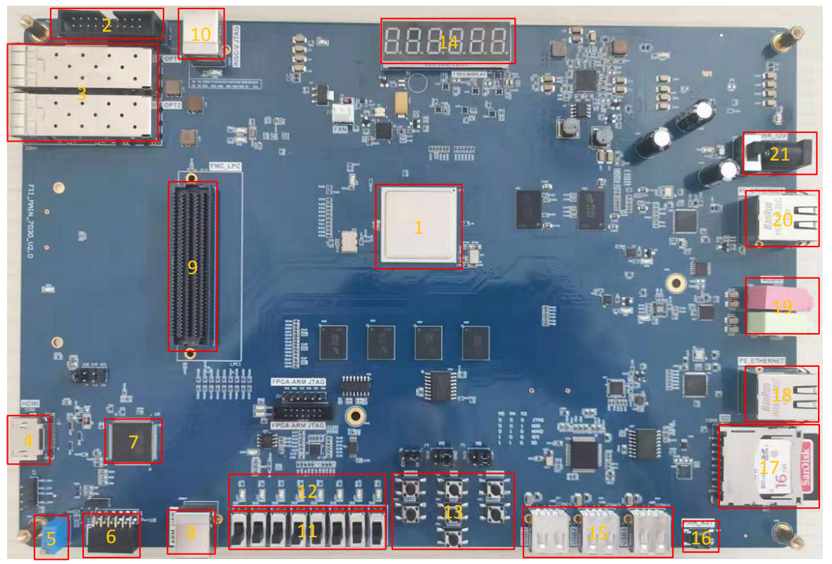
This part mainly guides the user to learn the development of FPGA program and the use of onboard hardware through the development example of FPGA.

At the same time, the application system software Xilinx is introduced from the elementary to the profound. The development exercises covered in this section are as follows:
Experiment 1: LED shifting design
Experiment 2: ILA experiment
Experiment 3: Segment display digital clock experiment
Experiment 4: button debouncing experiment
Experiment 5: digital clock comprehensive experiment
Experiment 6: use of multiplier and ISIM simulation
Experiment 7: hex to BCD conversion and application
Experiment 8: usage of ROM
Experiment 9: use dual-RAM to read and write frame data
Experiment 10: asynchrounous serial port design and experiment
Experiment 11: IIC transmission experiment
Experiment 12: HDMI experiment
Experiment 13: Ethernet experiment


