
Description
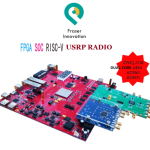
FII-PRX100-S Xilinx Risc-V FPGA Board is a ready-to-use development platform designed around the Field Programmable Gate Array (FPGA) from Xilinx. It was designed to cover all aspects of FPGA Development and Experiment, RISC-V SOC . The main application areas aim at smart home, Wearable, sensor Fusion, IOT, and industrial control etc.
FII-PRX100 Risc-V FPGA Board is a ready-to-use development platform designed around the Field Programmable Gate Array (FPGA) from Xilinx. It was designed to cover all aspects of FPGA Development and Experiment, RISC-V SOC . The main application areas aim at smart home, Wearable, sensor Fusion, IOT, and industrial control etc.
Features:
|
|
The entire system is designed by the verilog language, and all IPs can be added, deleted and reconfigured.
The FII-PRX100-S RISC-V development board introduction
- Suitable for FPGA study and training
- Fully support FIE310 CPU running and system development
- Suitable for user customized RV32G verification and validation
- JTAG interface for FPGA and FIE310 CPU download and debug
- Support Windows software and linux development environment
- GCC compilation toolchain and graphical software development environment
- Hardware resource: Switchs, Push Button ,USB to UART convertor, QSPI flash, I2C EEPROM, 100M/1G ethernet, USB keyboard mouse,GPIO , hdmi transmitter and camera etc.

RISC-V IPCore user development Guide
This document is edited by Fraser Innovation Inc. Step by step introduce how to develop each RISC-V CPU RTL modules based on RISC-V ISA, Simulations and board verifications, software environment and details on C language development, debug and program
Artificial Intelligence
Voice collection, speech recognition
Image acquisition and image recognition, deep learning
IOT
FII-PRX100 Risc-V FPGA Board Product Features:
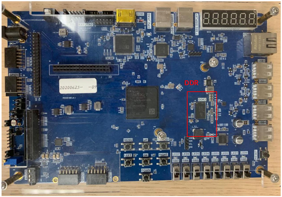
- FPGA part: XC7A100T-2FGG676I
- 1MSPS On-chip: yes
- Logic Cells: 101440
- Logic Slices: 15850
- Flip-flops: 65200
- Memory blocks(36K): 135
- Memory block(Kb): 4860
- Clock Management Tiles: 6
- DSP Slices: 240
System Features:
- ADC: On-chip analog-to-digital converter (XADC)
- Super Sram: IS61WV25616 (2 slices ) 256K x 32bit
- Spi Flash: serial flash (16M bytes)
- JTAG: jtag Programmable ports
- Multifunction: used for other board (For example: iMX226 camera board, or adv7612 Hdmi in board , etc)
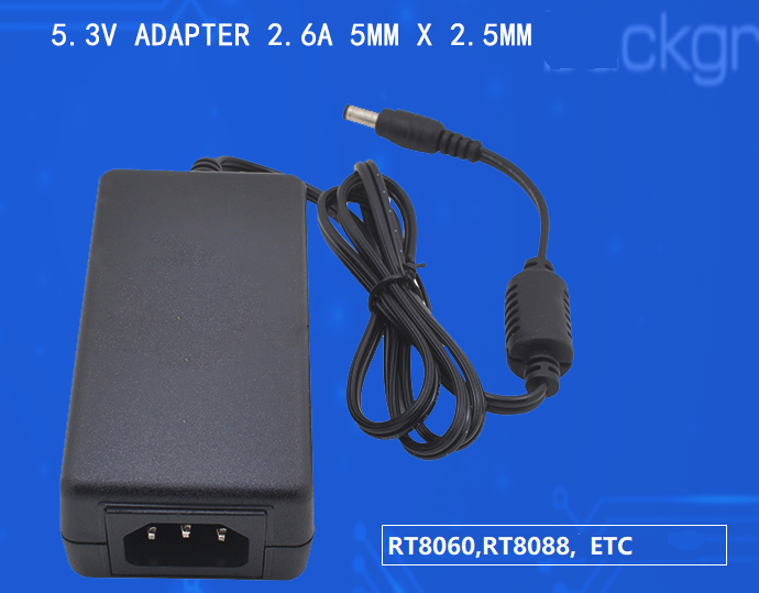
- Power Supply: 12V adapter source
Interaction and Sensory Devices:
- 8 Switches
- 7 Buttons (up , down, left, right, ok, menu, return)
- 1 Reset button
- 8 LEDs
- 1 4-digit 7 segment display
- 1 I2c interface (24c02 eeprom)
-
Expansion Connector:
- 4 gpio connectors (compatible with digilent Pmod)
- 2 MultiFunction connectors (connect with iMX226 board, or others)
- Main Chips: xilinx (1.0mm pitch) XC7A100T_FGG676
Interaction and Sensory Devices
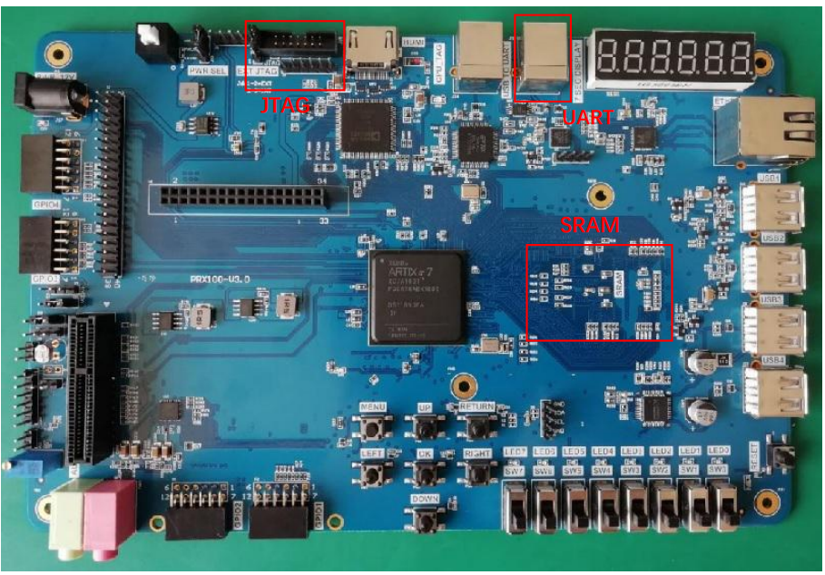
- GPIO Interface (16 ) 2×8 Standard 2.54mm connector (pin)
- led output (8 ) 0603 SMD
- 8 switchs SMD
- 7 buttons (Top, Bottom, left, right,center, top left (menu), top right (return)
- i2c 24c02 smd soic
- spi flash MX25L6433F 8-SOP (8M bytes)
- usb2uart ft2232C/H (2 uart ) Or cp2102 (1 uart)
- jtag 2×5 Standard 2.54mm connectors(pin)
- eth 1G CAT5 Ethernet (rtl8111e)
- sram IS61WV25616 (2 pieces ) 256K x 32bit
- Digital tube 7seg (4) oasistek TOF-5421BMRL-N
- Hdmi out adv7511, hdmi_adv7511.SchDoc
- Test Port: 1×6 Standard2.54mm Connectors (pin)
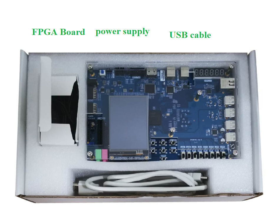
We will send you following Documents after you have bought from us:
Risc-V Board PRX100-S Experimental Manual
Risc-V Board PRX100-S Schematic Diagram
Risc-V Board PRX100-S Hardware Configuration
FII-PRX100 Development Board ( ARTIX 100T, XC7A100T, RISC-V FPGA Developing Board)
Online Shopping:
-
FII-PRX100-S RISC-V development board
- Suitable for FPGA study and training
- Fully support FIE310 CPU running and system development
- Suitable for user customized RV32G verification and validation
- JTAG interface for FPGA and FIE310 CPU download and debug
- Support Windows software and linux development environment
- GCC compilation toolchain and graphical software development environment
- Hardware resource: Switchs, Push Button ,USB to UART convertor, QSPI flash, I2CEEPROM, 100M/1G ethernet,USB keyboard mouse,GPIO, hdmi transmitter and camera etc.
1.System Design Objective
The main purpose of this system design is to complete FPGA learning, development and experiment with Xilinx-Vivado. The main device uses the Xilinx-XC7A100T-2FGG676I and is currently the latest generation of FPGA devices from Xilinx. The main learning and development projects can be completed as follows:
- Basic FPGA design training
- Construction and training of the SOPC (Microblaze) system
- IC design and verification, the system provides hardware design, simulation and verification of RISC-V CPU
- Development and application based on RISC-V
- The system is specifically optimized for hardware design for RISC-V system applications.
2.System Resource
-
- Extended memory
- Use two Super Srams in parallel to form a 32-bit data interface with a maximum access space of 1M bytes.
- IS61WV25616 (2 pieces) 256K x 32bit
- Serial flash
- Spi interface serial flash (128M bytes)
- Serial EEPROM
- Gigabit Ethernet: 100/1000 Mbps
- USB to serial interface: USB-UART bridge
3.Human-computer Interaction Interface
-
- 8 toggle switches
- 8 push buttons
- Definition of 7 push buttons: up, down, left, right, ok, menu, return
- 1 for rest: Reset button
- 8 LEDs
- 6 7-segment decoders
- I2C bus interface
- UART external interface
- JTAG programming interfaces
- Integrated FPGA Jtag and Risc-V Jtag by using single USB port.
- Built-in RISC-V IPCore
- CPU software debugger, no external RISC-V JTAG emulator required
- 12-pin GPIO connectors, in line with PMOD interface compatible.
4 Software Development System
- Vivado 18.1 and later version for FPGA development, Microblaze SOPC
- Freedom Studio-Win_x86_64 Software development for RISC-V CPU
5. Supporting Resources
-
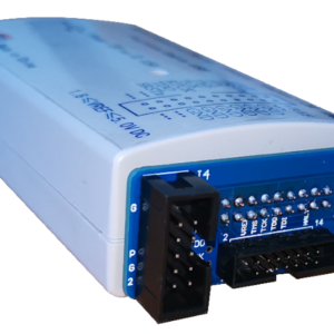
- RISC-V JTAG Debugger
- Xilinx Altera JTAG Download Debugger
- FII-PRX100 Development Guide
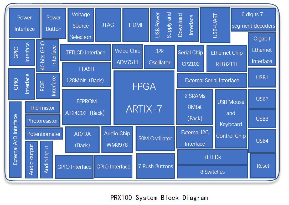
6. HareWare Resources
- 1 PCF8591 AD/DA conversion chip, reserved external interface, free input and output;
- Onboard 50MHz and 32.768kHz oscillators provide stable clock signals to the development board;
- 8-bit DIP switch;
- 8-bit LED;
- 1 128Mbit Flash chip;
- 4 GPIO external signal expansion interfaces, also the PMOD standard interface;
- A 40-pin GPIO expansion interface that provides a large amount of I/O for developers to use freely;
- Two JTAG interfaces, one for the FPGA download debug interface (J4, J5) and one for the RISC-V CPU JTAG debug interface(J16). Built-in RISC-V CPU software debugger, no external RISC-V JTAG emulator required;
- 1 UART asynchronous serial interface;
- 2 SRAMs with a capacity of 8Mbit;
- a pair of audio input and output interfaces;
- 1 PCIE interface;
- 4 USB interfaces, 2 for the mouse and keyboard interface, 2 for the universal serial interface;
- 1 USB (USB-B) to UART interface for serial communication;
- 1 TFTLCD touch screen interface, which can realize the display and operation of the touch screen;
-
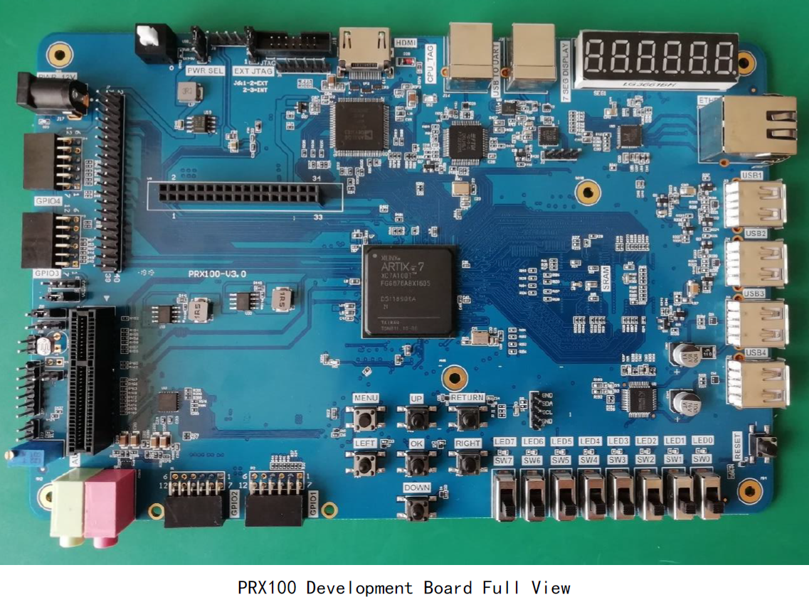
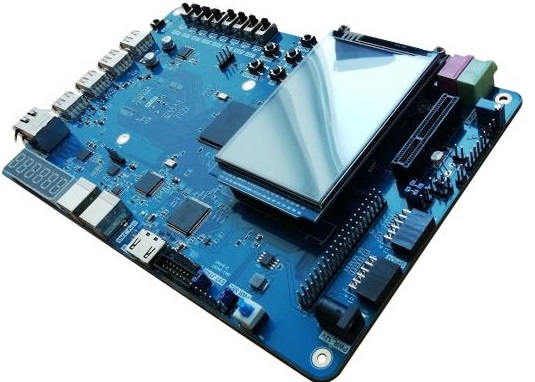
PRX100 Development Board Full View
RISC-V FPGA Board – FII-PRX100-S Experimental Manuals – Study Guide (V1.1)
-
-
- xilinx Risc-V FPGA Board – FII-PRX100 – Development System Introduction
- Risc-V FPGA Board Xilinx – Development Board Experiment 1 – LED Shifting – FII-PRX100
- Xilinx Risc-V Board Tutorial : Switches and Display – FII-PRX100 FPGA Board Experiment 2
- Xilinx Risc-V Board Tutorial : Basic Digital Clock Experiment and Programming of FPGA Configuration Files- FII-PRX100 FPGA Board Experiment 3
- Xilinx Risc-V Board Tutorial : Block/SCH Digital Clock Design- FII-PRX100 FPGA Board Experiment 4
- Xilinx Risc-V Board Tutorial : Button Debounce Design and Experimental- FII-PRX100 FPGA Board Experiment 5
- Xilinx Risc-V Board Tutorial : Digital Clock Comprehensive Design Experiment- FII-PRX100 FPGA Board Experiment 6
- Xilinx Risc-V Board Tutorial : Multiplier Use and ISIM Simulation- FII-PRX100 FPGA Board Experiment 7
- Xilinx Risc-V Board Tutorial : Hexadecimal Number to BCD Code Conversion and Application – FII-PRX100 FPGA Board Experiment 8
- Xilinx Risc-V Board Tutorial : Use of ROM – FII-PRX100 FPGA Board Experiment 9
- Xilinx Risc-V Board Tutorial : Use Dual_port RAM to Read and Write Frame Data – FII-PRX100 FPGA Board Experiment 10
- Xilinx Risc-V Board Tutorial : Asynchronous Serial Port Design and Experiment – FII-PRX100 FPGA Board Experiment 11
- Xilinx Risc-V Board Tutorial : IIC Protocol Transmission – FII-PRX100 FPGA Board Experiment 12
- Xilinx Risc-V Board Tutorial : AD, DA Experiment – FII-PRX100 FPGA Board Experiment 13
- Xilinx Risc-V Board Tutorial : HDMI Graphic Display Experiment – FII-PRX100 FPGA Board Experiment 14
- How ethernet work and familiar with MII, GMII, RGMII interface types – FII-PRX100 Risc-V Board Experiment 15
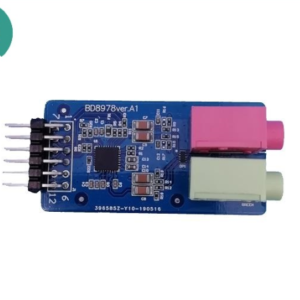
- Audio 8978 Loopback Experiment – What is I2S (Inter-IC Sound) bus and how it works – AWM8978 Audio Boardudio – Xilinx Risc-V FII-PRX100 Board Experiment 16
- Reading Experiment of Serial Port Partition of Static Memory SRAM, Read and write timing of IS61WV25616BLL SRAM, and prepare for the next experimental experiment of OV5640 camera experiment – – Xilinx Risc-V FII-PRX100 Board Experiment 17
- Photo Display Experiment of OV5640 Camera , Understand the power-on sequence of the OV5640 camera and the corresponding register configuration process – Xilinx Risc-V Board FII-PRX100 Experiment 18
- High-speed ADC9226 Acquisition Experiment – Xilinx Risc-V Board FII-PRX100 Experiment 19
-
-
The Newest Xilinx Risc-V Board FII-PRX100-S, FII-PRX100-D Experiment Manuals with 20 experiments.
- released_PRX100_hardware_configuration
FII_PRX100T_V3_20190720_NP
Reviews
There are no reviews yet.