
Description
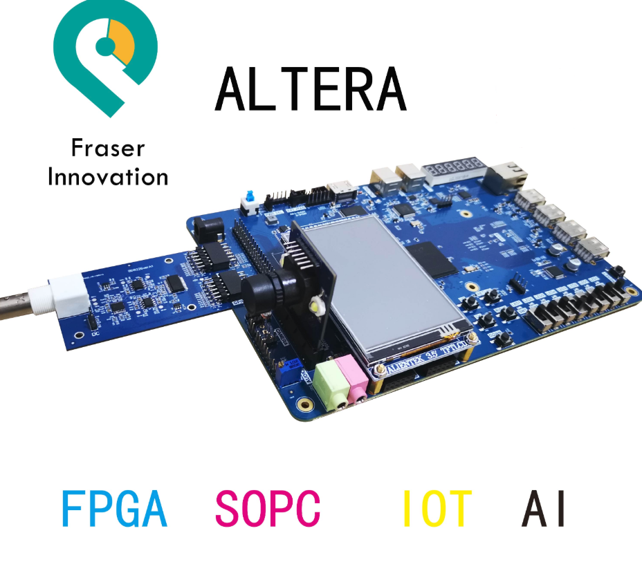
If you want Altera Risc-V Development Board, please check Following link:
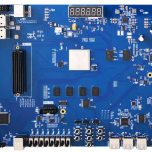
Risc-V FPGA Board – FII-PRA040 Altera risc-v SOPC AI Cyclone10
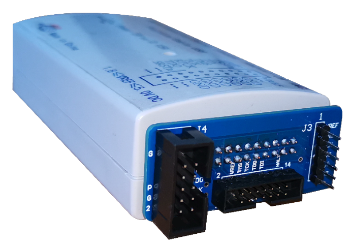
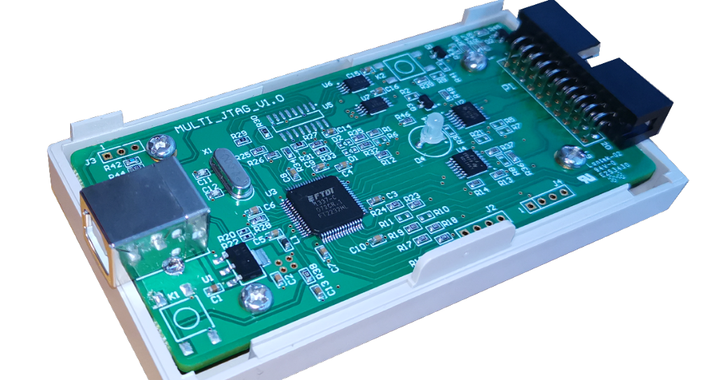
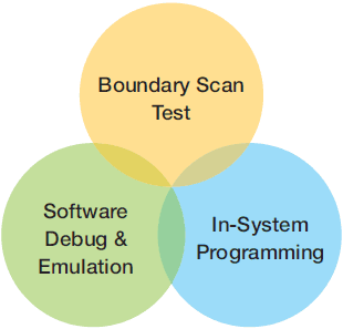
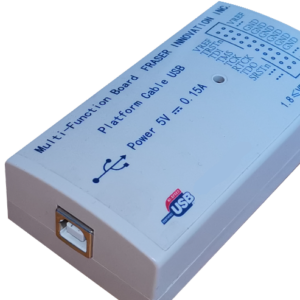
Following is the instruction about ALTERA FPGA RISC-V CPU Two-In-One JTAG.
- Debugs software for RISC-V CPU with JTAG interface supported by OpenOCD
- High speed USB 2.0 interface to local server.
- Standard 2×10 PINs JTAG connector with extension board adapt to 10PIN,14PIN and 6PIN target board
- Supports RISC-V target board voltage range 1.8 – 5.0 V DC
- Supported by the open-source community and OpenOCD debugger software
-
Well Runs on FreedomStudio IDE development packages, GCC C compiler, openOCD debugger
- Works with FreedomStudio for RISC-V via GDB server
- Supported in Windows, Linux and Mac
- Dimensions 10.2x5.4 mm (2×1.6″) , Adapter plate (6pin, 2x7pin 2.54mm,15 cm (8″) 2×10 JTAG cable , 1×6 JTAG cable , 2×7 JTAG cable ribbon cable are included.
About JTAG
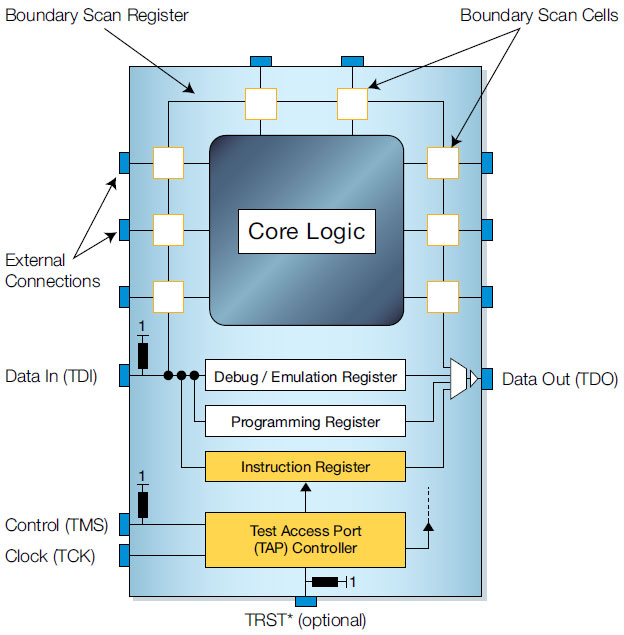
JTAG interface signals
There is a maximum of five lines that may be used for a JTAG interface, although one of them is optional and therefore may not always be present. This may be the case when the design becomes short of pins on a connector and the optional one can be sacrificed.
The signals that may be used are given below:
- TCK – Test Clock: The test clock pin on the JTAG interface is the clock signal used for ensuring the timing of the boundary scan system. The Test Clock is used to load the test mode data from the TMS pin, and the test data on the TDI pin on the rising edge. On the falling edge test clock outputs the test data on the TDO pin. It is important that the clock line is properly terminated to prevent reflections that may give rise to false triggering and incorrect operation of the JTAG interface.
- TDI – Test Data Input: The TDI pin on the JTAG interface or JTAG connector is the connection onto which the test instructions data stream is passed. It receives serial input data which is either feed to the test data registers or instruction register, dependent upon on the state of the TAP controller. The TDI line has an internal pull-up, and therefore the input is high with no input.
- TDO – Test Data Output: This pin within the JTAG interface provides data from the boundary scan registers, i.e. test data shifts out on this pin. It delivers serial data which comes from either the test data registers or instruction register, dependent upon on the state of the TAP controller. Data applied to the TDI pin will appear at the TDO pin but may be shifted by a number of clock cycles, depending on the length of the internal register. The TDO pin has a high-impedance.
- TMS – Test Mode Select: This input on the JTAG interface also clocks through on the rising edge of TCK determines the state of the TAP controller. It controls the operation of the test logic, by receiving the incoming data. The value at the input on the rising edge of the clock controls the movement through the states of the TAP controller. The TMS line has an internal pull-up, and therefore the input is high with no input.
- TRST – Test Reset: This is an optional active low test reset pin on the JTAG interface. It permits asynchronous TAP controller initialization without affecting other device or system logic. The TRST signal is usually asynchronous, but not always so dependent upon the particular device in question.If a TRST connection is not available, then the test logic can be reset by using TCK and TMS in a synchronous fashion. Note that resetting test logic does not imply resetting other circuits: there are generally processor-specific JTAG operations which are able to reset all or part of the device being tested.
JTAG Technologies solutions for programming embedded memories of Microprocessors and DSPs are also known as SCIP (Serial Controlled IC Programmer) modules. The family comprises a wide range of software modules that can be used by test and production engineers to broaden the scope of their in-system device programming facilities without adding much or anything in the way of additional interface hardware.
While many devices have standardised on JTAG (IEEE Std 1149.1) as hardware interface for programming and testing there has been little in the way of standardisation regarding the way internal (flash) memories are programmed. The use of ‘Private’ instructions and non-standard state machine implementations have meant that some JTAG/boundary-scan tool-sets are unable to cope with the variety of devices that now use JTAG as their programming interface. Furthermore there exists a secondary layer of devices that use other, often lower pin count, interfaces to support their programming. Examples of these alternative interfaces are BDM, SPI, SWD (ARM Single Wire Debug) etc.. JTAG Technologies SCIP modules overcome these obstacles.
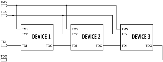
A JTAG interface is a special interface added to a chip. Depending on the version of JTAG, two, four, or five pins are added. The four and five pin interfaces are designed so that multiple chips on a board can have their JTAG lines daisy-chained together if specific conditions are met. The two pin interface is designed so that multiple chips can be connected in a star topology. In either case a test probe need only connect to a single “JTAG port” to have access to all chips on a circuit board.
Daisy-chained JTAG (IEEE 1149.1)
The connector pins are:
- TDI (Test Data In)
- TDO (Test Data Out)
- TCK (Test Clock)
- TMS (Test Mode Select)
- TRST (Test Reset) optional.
The TRST pin is an optional active-low reset to the test logic, usually asynchronous, but sometimes synchronous, depending on the chip. If the pin is not available, the test logic can be reset by switching to the reset state synchronously, using TCK and TMS. Note that resetting test logic doesn’t necessarily imply resetting anything else. There are generally some processor-specific JTAG operations which can reset all or part of the chip being debugged.
Since only one data line is available, the protocol is serial. The clock input is at the TCK pin. One bit of data is transferred in from TDI, and out to TDO per TCK rising clock edge. Different instructions can be loaded. Instructions for typical ICs might read the chip ID, sample input pins, drive (or float) output pins, manipulate chip functions, or bypass (pipe TDI to TDO to logically shorten chains of multiple chips).
As with any clocked signal, data presented to TDI must be valid for some chip-specific Setup time before and Hold time after the relevant (here, rising) clock edge. TDO data is valid for some chip-specific time after the falling edge of TCK.
The maximum operating frequency of TCK varies depending on all chips in the chain (the lowest speed must be used), but it is typically 10-100 MHz (100-10 ns per bit). Also TCK frequencies depend on board layout and JTAG adapter capabilities and state. One chip might have a 40 MHz JTAG clock, but only if it is using a 200 MHz clock for non-JTAG operations; and it might need to use a much slower clock when it is in a low power mode. Accordingly, some JTAG adapters have adaptive clocking using an RTCK (Return TCK) signal. Faster TCK frequencies are most useful when JTAG is used to transfer lots of data, such as when storing a program executable into flash memory.
Clocking changes on TMS steps through a standardized JTAG state machine. The JTAG state machine can reset, access an instruction register, or access data selected by the instruction register.
JTAG platforms often add signals to the handful defined by the IEEE 1149.1 specification. A System Reset (SRST) signal is quite common, letting debuggers reset the whole system, not just the parts with JTAG support. Sometimes there are event signals used to trigger activity by the host or by the device being monitored through JTAG; or, perhaps, additional control lines.
Even though few consumer products provide an explicit JTAG port connector, the connections are often available on the printed circuit board as a remnant from development prototyping and/or production. When exploited, these connections often provide the most viable means for reverse engineering.
Jtag Uses
- Except for some of the very lowest end systems, essentially all embedded systems platforms have a JTAG port to support in-circuit debugging and firmware programming as well as for boundary scan testing:
- ARM architecture processors come with JTAG support, sometimes supporting a two-wire “SWD” variant or high speed tracing of traffic on instruction or data busses.
- Modern 8-bit and 16-bit microcontroller chips, such as Atmel AVR and TI MSP430 chips, support JTAG programming and debugging. However, the very smallest chips may not have enough pins to spare (and thus tend to rely on proprietary single-wire programming interfaces); if the pin count is over 32, there is probably a JTAG option.
- Almost all FPGAs and CPLDs used today can be programmed via a JTAG port. A Standard Test and Programming Language is defined by JEDEC standard JESD-71 for JTAG programming of PLD’s.
- Many MIPS and PowerPC processors have JTAG support
- Intel Core, Xeon, Atom, and Quark processors all support JTAG probe mode with Intel specific extensions of JTAG using the so-called 60-pin eXtended Debug Port [XDP]. Additionally the Quark processor supports more traditional 10-pin connectors.
- Consumer products such as networking appliances and satellite television integrated receiver/decoders often use microprocessors which support JTAG, providing an alternate means to reload firmware if the existing bootloader has been corrupted in some manner.
- The PCI bus connector standard contains optional JTAG signals on pins 1-5; PCI Express contains JTAG signals on pins 5-9.[18] A special JTAG card can be used to reflash a corrupt BIOS.
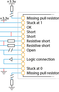
- Boundary scan testing and in-system (device) programming applications are sometimes programmed using the Serial Vector Format, a textual representation of JTAG operations using a simple syntax. Other programming formats include ‘JAM’ and STAPL plus more recently the IEEE Std. 1532 defined format ‘ISC’ (short for In-System Configuration). ISC format is used in conjunction with enhanced BSDL models for programmable logic devices (i.e. FPGAs and CPLDs) that include addition ISC_<operation> instructions in addition to the basic bare minimum IEEE 1149.1 instructions. FPGA programming tools from Xilinx, Altera, Lattice, Cypress, Actel, etc. typically are able to export such files.
- As mentioned, many boards include JTAG connectors, or just pads, to support manufacturing operations, where boundary scan testing helps verify board quality (identifying bad solder joints, etc.) and to initialize flash memory or FPGAs.
- JTAG can also support field updates and troubleshooting.
Jtag Connectors
There are no official standards for JTAG adapter physical connectors. Development boards usually include a header to support preferred development tools; in some cases they include multiple such headers, because they need to support multiple such tools. For example, a microcontroller, FPGA, and ARM application processor rarely shares tools, so a development board using all of those components might have three or more headers. Production boards may omit the headers, or when space is limited may provide JTAG signal access using test points.
Some common pinouts for 2.54 mm (0.100 in) pin headers are:
ARM 2×10 pin (or sometimes the older 2×7), used by almost all ARM based systems
MIPS EJTAG (2×7 pin) used for MIPS based systems
2×5 pin Altera ByteBlaster-compatible JTAG extended by many vendors
2×5 pin AVR extends Altera JTAG with SRST (and in some cases TRST and an event output)
2×7 pin Texas Instruments used with DSPs and ARM-based products such as OMAP
8 pin (single row) generic PLD JTAG compatible with many Lattice ispDOWNLOAD cables
MIPI10-/20-connectors (1.27 mm 050″) for JTAG, cJTAG and SWD
Those connectors tend to include more than just the four standardized signals (TMS, TCK, TDI, TDO). Usually reset signals are provided, one or both of TRST (TAP reset) and SRST (system reset). The connector usually provides the board-under-test’s logic supply voltage so that the JTAG adapters use the appropriate logic levels. The board voltage may also serve as a “board present” debugger input. Other event input or output signals may be provided, or general purpose I/O (GPIO) lines, to support more complex debugging architectures.
Higher end products frequently use dense connectors (frequently 38-pin MICTOR connectors) to support high-speed tracing in conjunction with JTAG operations. A recent trend is to have development boards integrate a USB interface to JTAG, where a second channel is used for a serial port. (Smaller boards can also be powered through USB. Since modern PCs tend to omit serial ports, such integrated debug links can significantly reduce clutter for developers.) Production boards often rely on bed-of-nails connections to test points for testing and programming.
Reviews
There are no reviews yet.