
Description
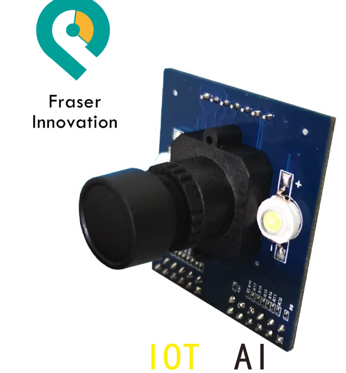
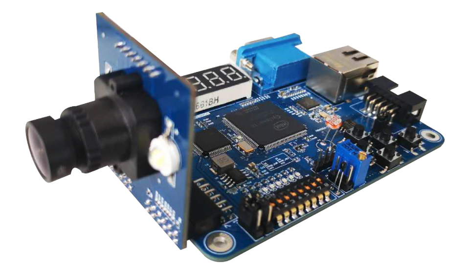
Fraser Innovation Inc develops BD5640 that contains a video camera based on video sensor OV5640 (CMOS). BD5640 support PMOD connector and it is compatible with different kinds of FII developing boards.
1.Introduction
The FII-BD5640-PMOD is a camera module designed to integrate the Omnivision ov5640 5 megapixel (MP) color image sensor , with its compatible power supply and oscillator. This board can be used with different kinds of FII FPGA development boards. Power supply for BD5640 is 3V3. The sensor includes lots of internal processing functions that can adjust white balance, saturation, hue, sharpness, and gamma correction.
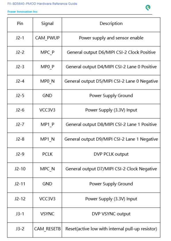
The output data interface support general Digital output interface and dual-lane MIPI CSI-2 interface, so it can provides enough data bandwidth for common video streaming formats such as 1080p and 720p. The ov5640 (color) image sensor uses DVP data interface and SCCB control interface.
2.Basic Features
- 5MP color system-on-chip image sensor
- General digital output and Dual lane MIPI CSI-2 image sensor interface
- Supports QSXGA@15hz, 1080p@30Hz, 720p@60Hz,VGA@90Hz and QVGA@120Hz
- Output format include RAW10, RGB565, CCIR656, YUV422/420, YCbCr422, and JPEG compression
- M12 22mm lens mount with M12 3.6mm focus lens
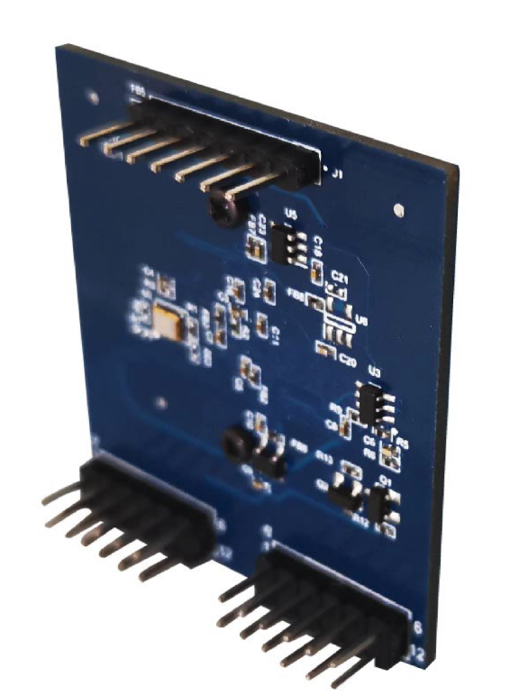
- Small PCB size for flexible designs (40mm*44mm)
- Powered up from double standard PMOD connector
- Supports FII-7030 and other FII FPGA development boards
After you have purchase, we will send you:
- OV5640 Datasheet
- Schematic
- OV5640 Hardware Reference Guide
You can also check our another Product:
4k 500M Camera Module – ov5640 – FII-BD5640 PCIE Interface
What is OV5640 ?
ov5640 is a 1/4-inch, 5-Megapixel SOC Image Sensor which is developed by OmniVision Technologies Inc.
The OV5640 delivers a complete 5-megapixel camera solution on a single chip, aimed at offering cost efficiencies that serve the high- volume autofocus (AF) camera phone market. The system-on-a- chip (SOC) sensor features OmniVision’s 1.4 micron OmniBSI™ backside illumination architecture to deliver excellent pixel performance and best-in-class low-light sensitivity, while enabling ultra compact camera module designs of 8.5 mm x 8.5 mm with <6 mm z-height.
The OV5640 provides the full functionality of a complete camera, including anti-shake technology, AF control, and MIPI while being easier to tune then two-chip solutions, making it an ideal choice in terms of cost, time-to-market and ease of platform integration.
The OV5640 enables 720p HD video at 60 frames per second (fps) and 1080p HD video at 30 fps with complete user control over formatting and output data transfer. The 720p/60 HD video is captured in full field of view (FOV) with 2 x 2 binning, which doubles the sensitivity and improves the signal-to-noise ratio (SNR). Additionally, a unique post-binning re-sampling filter function removes zigzag artifacts around slant edges and minimizes spatial artifacts to deliver even sharper, crisper color images. To further improve camera performance and user experience, the OV5640 features an internal anti-shake engine for image stabilization, and it supports Scalado™ tagging for faster image preview and zoom.
The OV5640 offers a digital video port (DVP) parallel interface and a high-speed dual lane MIPI interface, supporting multiple output formats. An integrated JPEG compression engine simplifies data transfer for bandwidth-limited interfaces. The sensor’s automatic image control functions include automatic exposure control (AEC), automatic white balance (AWB), automatic band filter (ABF), 50/60 Hz automatic luminance detection, and automatic black level calibration (ABLC). The OV5640 delivers programmable controls for frame rate, AEC/AGC 16-zone size/position/weight control, mirror and flip, cropping, windowing, and panning. It also offers color saturation, hue, gamma, sharpness (edge enhancement), lens correction, defective pixel canceling, and noise canceling to improve image quality.
OV5640 Application
-
- MobilePhones
- Digital Still and Video Cameras
- Entertainment
OV5640 Product Features
- ¬1.4 µm x 1.4 µm pixel with OmniBSI ¬ support horizontal binning and technology for high performance (high vertical sub-sampling sensitivity, low crosstalk, low noise,
improved quantum efficiency) - ¬ post binning resampling filter to minimize spatial/aliasing artifacts
¬optical size of 1/4″ on 2×2 binned image - ¬automatic image control functions: ¬ embedded JPEG compression
– automatic exposure control (AEC)
– automatic white balance (AWB) ¬ support for anti-shake
– automatic band filter (ABF)
– automatic 50/60 Hz luminance detection ¬ digital video port (DVP) parallel output
– automatic black level calibration (ABLC) interface and dual lane MIPI output interface
¬programmable controls for frame rate, AEC/AGC 16-zone size/position/ ¬ embedded 1.5V regulator for core weight control, mirror and flip, cropping, power windowing, and panning
¬programmable I/O drive capability,
¬image quality controls: color saturation, I/O tri-state configurability hue, gamma, sharpness (edge enhancement), lens correction, defective ¬ support for black sun cancellation pixel canceling, and noise canceling
¬embedded arbitrary scalar supporting
¬support for output formats: RAW RGB, any size from 5 MP and below RGB565/555/444, CCIR656, YUV422/420, YCbCr422, and ¬ auto focus control (AFC) with compression embedded AF VCM driver - ¬support for LED and flash strobe mode ¬ embedded microcontroller
- ¬support for internal and external frame ¬ suitable for module size of synchronization for frame exposure 8.5 x 8.5 x <6mm with both CSP and mode RW packaging
- ¬support horizontal binning and vertical sub-sampling
Product Specifications
active array size: 2592 x 1944
power supply:
– core: 1.5 V ±5% (with embedded 1.5 V regulator)
– analog: 2.6 ~ 3.0 V (2.8 V typical)
– I/O: 1.8 V / 2.8 V
power requirements:
-
-
-
- -active:140 mA
- -standby: 20 µA
-
-
temperature range:
-operating:-30°C to 70°C junction
-stable image: 0°C to 50°C junction
output formats: 8/10-bit RAW RGB output
lens size: 1/4″
lens chief ray angle: 24°
input clock frequency: 6 ~ 27 MHz
shutter: rolling shutter / frame exposure
maximumimage transfer rate:
QSXGA (2592×1944): 15 fps
1080p: 30 fps
1280 x 960: 45 fps
720p: 60 fps
VGA (640×480): 90 fps
QVGA (320×240): 120 fps
sensitivity: 600 mV/lux-sec
maximum exposure interval: 1964 x tROW
max S/N ratio: 36 dB
dynamic range: 68 dB @ 8x gain
pixel size: 1.4 µm x 1.4 µm
dark current: 8 mV/sec @ 60°C junction temperature
image area: 3673.6 µm x 2738.4 µm
package dimensions:
– CSP3: 5985 µm x 5835 µm
– COB: 6000 µm x 5850 µm
OV5640 Functional Block Diagram
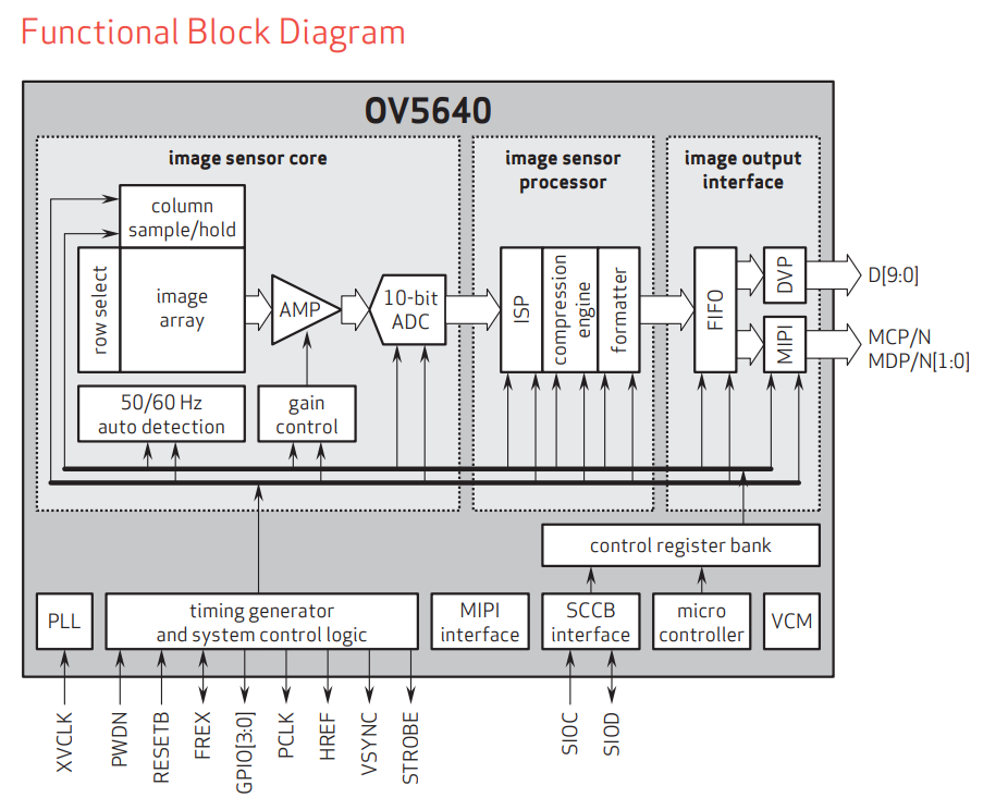
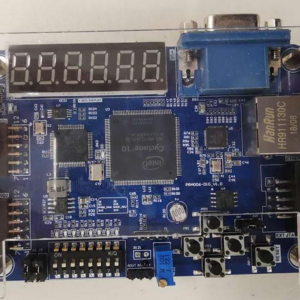
Photo Display Experiment of OV5640 Camera
Experiment 17 Photo Display Experiment of OV5640 Camera
17.1 Experiment Objective
- Understand the power-on sequence of the OV5640 camera and the corresponding register configuration process when outputting images of different resolutions
- Review previous knowledge of IIC bus
- Review previous knowledge of HDMI
17.2 Experiment Implement
- Read the power-on sequence of the OV5640 datasheet, and correctly write the power-on control program according to the peripheral module schematics.
- Correctly write the configuration program of the OV5640 camera with a resolution of 640X480 according to the timing requirements of the SCCB interface
- Based on previous experiments, write a program to store the image data collected by 5640 in the development board SRAM.
- Write a program to display the image stored in the SRAM to the monitor via HDMI.
- The refresh of the image is controlled by the keys, and the screen display image is updated every time pressing it, similar to a camera.
17.3 Experiment
Some main procedures are given below. Refer the project file for the complete program
- Ov5640 power-on initialization program design is based on the power-on timing diagram of 5640 when connected to DVDD. Shown in Figure 17.1.

Figure 17.1 5640 power-on sequence
Power-on sequence program is as follows:
| module power_on_delay(clk_50M,reset_n_r,camera_pwup,initial_en,cam_resetb);
input clk_50M; input reset_n_r; output camera_pwup; output initial_en; (*mark_debug=”true”*)output reg cam_resetb =0; (*mark_debug=”true”*)reg [31:0]cnt1=0; reg initial_en=0; reg camera_pwup_reg=0; reg reset_n =0; assign camera_pwup=camera_pwup_reg; always @ (posedge clk_50M) reset_n<=reset_n_r ; //5ms, delay from sensor power up stable to Pwdn pull down always@(posedge clk_50M) begin if(reset_n==1’b0) cnt1<=0; else begin if (cnt1<50000000) cnt1<=cnt1+1 ; else cnt1<=cnt1 ; end end always@(posedge clk_50M) begin if(reset_n==1’b0) begin camera_pwup_reg<=0; end else begin if (cnt1==15000000) camera_pwup_reg<=1; else camera_pwup_reg<=camera_pwup_reg; end end always@(posedge clk_50M) begin if(reset_n==1’b0) begin cam_resetb <=0; end else begin if (cnt1==35000000) cam_resetb <=1; else cam_resetb <=cam_resetb ; end end always@(posedge clk_50M) begin if(reset_n==1’b0) begin initial_en<=0; end else begin if (cnt1==48000000) initial_en<=1; else initial_en<=initial_en; end end endmodule |
- 5640 chip configuration program
For more information, please check
Photo Display Experiment of OV5640 Camera
If you have any questions, you can contact us or post in the Sub-Board product forums. If you can not register to post, please let us know and I will create a forum username for you.
Reviews
There are no reviews yet.