

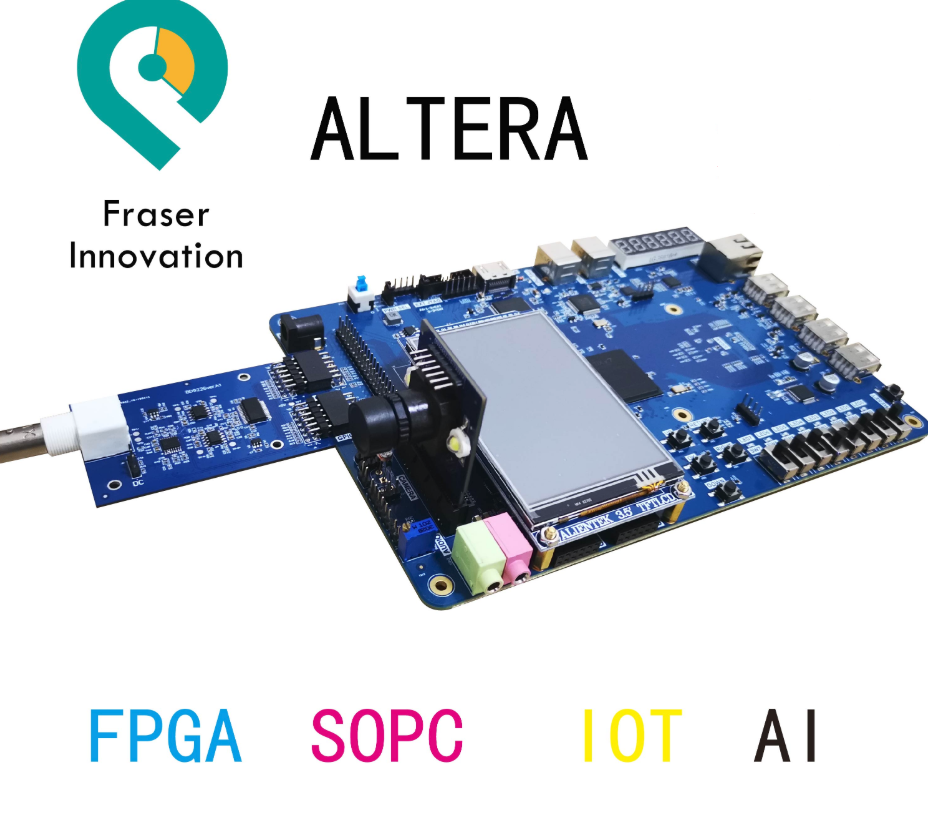
Altera Risc-V FPGA Board risc-v SOPC AI Cyclone10 – FII-PRA040 – RiscV Educational Platform

RISC-V Board ( ARTIX 100T, XC7A100T ) – FII-PRX100-D – Xilinx Risc-V FPGA Board ( RISC-V SOPC AI Xilinx artix-7 DRAM)

RISC-V Board ( ARTIX 100T, XC7A100T ) – FII-PRX100-S – Xilinx Risc-V FPGA Board ( riscv SOPC AI Xilinx artix-7 SRAM)

Risc-V FPGA Boards, Risc-V Learning Boards – Step by Step teaching you how to code in RISC-V machine
FII-PRX100 RISC-V development board
- Suitable for FPGA study and training
- Fully support FIE310 CPU running and system development
- Suitable for user customized RV32G verification and validation
- JTAG interface for FPGA and FIE310 CPU download and debug
- Support Windows software and linux development environment
- GCC compilation toolchain and graphical software development environment
- Hardware resource: Switchs, Push Button ,USB to UART convertor, QSPI flash, I2C EEPROM, 100M/1G ethernet, USB keyboard mouse,GPIO , hdmi transmitter and camera etc.
System Design Objective
The main purpose of this system design is to complete FPGA learning, development and experiment with Xilin-Vivado. The main device uses the Xilinx-XC7A100T-2FGG676I and is currently the latest generation of FPGA devices from Xilinx. The main learning and development projects can be completed as follows:
- Basic FPGA design training
- Construction and training of the SOPC (Microblaze) system
- IC design and verification, the system provides hardware design, simulation and verification of RISC-V CPU
- Development and application based on RISC-V
- The system is specifically optimized for hardware design for RISC-V system applications
2. System Resource
- Extended memory
- Use two Super Srams in parallel to form a 32-bit data interface with a maximum access space of 2M bytes.
- IS61WV51216 (2 pieces) 512K x 32bit
- Serial flash
- Spi interface serial flash (128M bytes)
- Serial EEPROM
- Gigabit Ethernet: 100/1000 Mbps
- USB to serial interface: USB-UART bridge
3. Human-computer Interaction Interface
- 8 toggle switches
- 8 push buttons
- Definition of 7 push buttons: up, down, left, right, ok, menu, return
- 1 for rest: Reset button
- 8 LEDs
- 6 7-segment decoders
- I2C bus interface
- UART external interface
- Two JTAG programming interfaces
- One is for downloading the FPGA debug interface, and the other one is the JTAG debug interface for the RISC-V CPU
- Built-in RISC-V
- CPU software debugger, no external RISC-V JTAG emulator required
- 12-pin GIPIO connectors, in line with PMOD interface standards
4 Software Development System
- Vivado 18.1 and later version for FPGA development, Microblaze SOPC
- Freedom Studio-Win_x86_64 Software development for RISC-V CPU
5. Supporting Resources
-
- RISC-V JTAG Debugger
- xilinx Altera JTAG Download Debugger
- FII-PRX100 Development Guide

Click Here to Buy Xilinx Risc-V FPGA Board FII-PRX100
The Risc-V Learning Tutors for PRX100 Risc-V FPGA Boards:
- Risc-V Board Tutorial : HDMI Graphic Display Experiment – FII-PRX100 FPGA Board Experiment 14
- Risc-V Board Tutorial : AD, DA Experiment – FII-PRX100 FPGA Board Experiment 13
- Risc-V Board Tutorial : IIC Protocol Transmission – FII-PRX100 FPGA Board Experiment 12
- Risc-V Board Tutorial : Asynchronous Serial Port Design and Experiment – FII-PRX100 FPGA Board Experiment 11
- Risc-V Board Tutorial : Use Dual_port RAM to Read and Write Frame Data – FII-PRX100 FPGA Board Experiment 10
- Risc-V Board Tutorial : Use of ROM – FII-PRX100 FPGA Board Experiment 9
- Risc-V Board Tutorial : Hexadecimal Number to BCD Code Conversion and Application – FII-PRX100 FPGA Board Experiment 8
- Risc-V Board Tutorial : Multiplier Use and ISIM Simulation- FII-PRX100 FPGA Board Experiment 7
- Risc-V Board Tutorial : Digital Clock Comprehensive Design Experiment- FII-PRX100 FPGA Board Experiment 6
- Risc-V Board Tutorial : Button Debounce Design and Experimental- FII-PRX100 FPGA Board Experiment 5
- Risc-V Board Tutorial : Block/SCH Digital Clock Design- FII-PRX100 FPGA Board Experiment 4
- Risc-V Board Tutorial : Basic Digital Clock Experiment and Programming of FPGA Configuration Files- FII-PRX100 FPGA Board Experiment 3
- Risc-V Board Tutorial : Switches and Display – FII-PRX100 FPGA Board Experiment 2
- Risc-V FPGA Board – Development Board Experiment 1 – LED Shifting – FII-PRX100
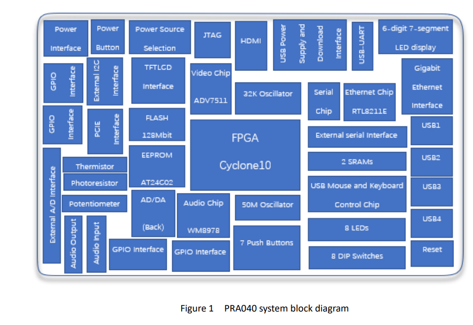
Altera Risc-V Board Two: FII-PRA040 Altera risc-v SOPC AI Cyclone10
FII-PRA040 Risc-V Educational Platform is a ready-to-use development platform designed around the Field Programmable Gate Array (FPGA) from Intel Altera.
It was designed for use in all fields of FPGA development and experiments.
Communication
Digital Communication DSP(FPGA)
Network
100M/1G Interface,switch VLAN
USB:
USB2.0 Engine Development
CPU:
RISC-V CPU 32bit Ecosystem Dvelopment and Educational Experiments
Artificial Intelligence
Voice collection, speech recognition Image acquisition and image recognition, deep learning
1、Design Objective of the System
The main purpose of this system design is to complete FPGA learning, development and experiment with Intel Quartus. The main device uses the Inte Cyclone10 10CL040YF484C8G and is currently the latest generation of FPGA devices from Intel. The major learning and development projects can be completed as follows:
- Basic FPGA design training
- Construction and training of the SOPC (NiosII) system
- IC design and verification, the system provides hardware design, simulation and verification of RISC-V CPU
- Development and application based on RISC-V
- The system is specifically optimized for hardware design for RISC-V system applications
2、System Resource
- Extended memory: Two Super Sram (IS61WV51216, 512K x 32bit) are connected in parallel to form a 32-bit data interface, and the maximum access space is up to 2M bytes.
- Serial flash: Spi interface serial flash (16M bytes)
- Serial EEPROM
- Gigabit Ethernet: 100/1000 Mbps
- USB to serial interface: USB-UART bridge
3、Human-computer Interaction Interface
- 8 DIP switches
- 8 push buttons, definition of 7 push buttons: MENU, UP, RETUN, LEFT, OK, RIGHT, DOWN, 1 for reset: RESET
- 8 LEDs
- 6 7-segment LED display
- I2C bus interface
- UART external interface
- Two JTAG programming interfaces: One is for downloading the FPGA debug interface, and the other is the JTAG debug interface for RISC-V CPU
- Built-in RISC-V CPU software debugger, no external RISC-V JTAG emulator required
- 4 12-pin GPIO connectors, in line with PMOD interface standards
4、Software Development System
- Quartus 18.0 and later version for FPGA development, Nios-II SOPC
- Freedom Studio-Win_x86_64 software development for RISC-V CPU
5、Supporting Resources
RISC-V JTAG Debugger
Intel Altera JTAG Download Debugger
FII-PRA040 User Experimental Manual
FII-PRA040 Hardware Reference Guide
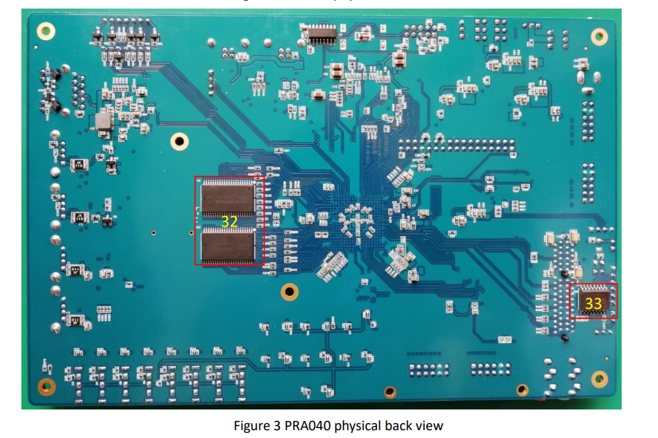
6、Physical Picture
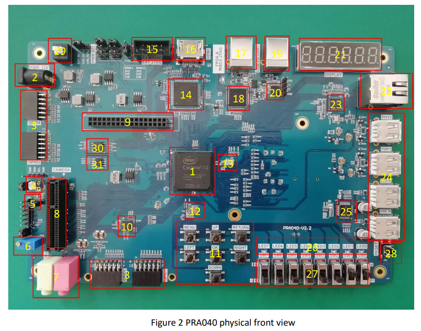
Corresponding to the physical picture, the main devices on board are as follows:
1、10CL040YE484C8G chip
2、External 12V power interface
3、GPIO interface
4、Thermistor (NTC-MF52)
5、Photoresistor
6、Potentiometer
7、Audio output (green), audio input (red)
8、PCIE interface
9、TFTCLD interface
10、Audio chip (WM8978)
11、7 push buttons
12、50M system clock
14、Video chip(ADV7511)
15、External JTAG download interface
16、HDMI interface
17、USB power supply and download interface
18、FPGA and RISC_V JTAG download chips (FT2232)
19、USB_UART interface
20、Serial chip (CP2102)
21、6 7-segment LED display
22、Ethernet interface
23、Ethernet PHY chip (RTL8211E-VB)
24、4 USB interfaces
25、USB mouse and keyboard control chip
26、8 LEDs
27、8-bit DIP switch
28、Reset button
29、Power button
30、Flash (N25Q128A,128M bit/16M bytes)
31、EEPROM (AT24C02N)
32、Two SRAMs
33、AD/DA conversion chip (PCF8591)
The Altera Risc-V FPGA Board Tutor – PRA040
- Altera Risc-V FPGA Tutorial : Use Dual-port RAM to Read and Write Frame Data – FII-PRA040 FPGA Board Experimental 9
- Altera Risc-V FPGA Tutorial : Use of ROM – FII-PRA040 FPGA Board Experimental 8
- Altera Risc-V FPGA Tutorial : Hexadecimal Number to BCD Code Conversion and Application – FII-PRA040 FPGA Board Experimental 7
- Altera Risc-V FPGA Tutorial : Use of Multipliers and ModelSim – FII-PRA040 FPGA Board Experimental 6
- Altera Risc-V FPGA Tutorial : Button Debounce – FII-PRA040 FPGA Board Experimental 5
- Altera Risc-V FPGA Tutorial : Block/SCH – FII-PRA040 FPGA Board Experimental 4
- Altera Risc-V FPGA Tutorial : Segment Display – FII-PRA040 FPGA Board Experimental 3
- Altera Risc-V FPGA Tutorial : SignalTap – FII-PRA040 FPGA Board Experimental 2
- Altera Risc-V FPGA Tutorial : LED shifting – FII-PRA040 FPGA Board Experimental 1
- Altera Risc-V FPGA Board Tutorial : Introduction of FII-PRA040 Development System
For DPF instruction how to code in Risc-V board, please check the product pages. If you buy one of our products, we will send you detail updated instruction step by step.
Click to Buy Altera Risc-V FPGA Board
RISC-V (pronounced “risk-five”) is an open-source hardware instruction set architecture (ISA) based on established reduced instruction set computer (RISC) principles.The project began in 2010 at the University of California, Berkeley, but many contributors are volunteers not affiliated with the university.
As of March 2019, version 2.2 of the user-space ISA is frozen, permitting most software development to proceed. The privileged ISA is available as draft version 1.10. A debug specification is available as a draft version 0.13.1
What is the license model of RISC-V?
The RISC-V ISA is free and open with a permissive license for use by anyone in all types of implementations. Designers are free to develop proprietary or open source implementations for commercial or other exploitations as they see fit. The RISC-V Foundation encourages all implementations that are compliant to the specifications.Note that the use of the RISC-V trademark requires a license which is granted to members of the RISC-V Foundation for use with compliant implementations. The RISC-V specification is based around a structure which allows flexibility with modular extensions and additional custom instructions/extensions. If an implementation was based on the RISC-V specification but includes modifications beyond this framework, then it cannot be referenced as RISC-V. https://riscv.org/faq/
RISC-V started in 2010 at the University of California at Berkeley Par Lab Project, which needed an instruction set architecture that was simple, efficient, and extensible and had no constraints on sharing with others. So Krste Asanovic (a founder of SiFive), Andrew Waterman, Yunsup Lee, and David Patterson created RISC-V. They built their first chip in 2011. In 2014, they announced it and gave it to the community.
SiFive has the widest family of RISC-V cores on the market and has been evangelizing them around the world.