
Description
FII-PRA040 RiscV Educational Platform is a ready-to-use development platform designed around the Field Programmable Gate Array (FPGA) from Intel Altera. RISC-V (pronounced “risk-five”) is an open-source hardware instruction set architecture (ISA) based on established reduced instruction set computer (RISC) principles.
It was designed for use in all fields of FPGA development and experiments.
Communication
Digital Communication DSP(FPGA)
Network
100M/1G Interface,switch VLAN
USB:
USB2.0 Engine Development
CPU:
RISC-V CPU 32bit Ecosystem Dvelopment and Educational Experiments
Artificial Intelligence
Voice collection, speech recognition Image acquisition and image recognition, deep learning
Features
| 10CL040 | 10CL080 | |
| Logic elements (LEs) (K) | 40 | 80 |
| Memory blocks(9K) | 126 | 305 |
| LMemory block(Kb) | 1134 | 2745 |
| 18×18 multipliers | 126 | 244 |
| Phase-locked loop(PLL) | 4 | 4 |
| Global clock networks | 20 | 20 |

System Features:
-
- Sram: IS61WV25616 (2 pieces ) 256K x 32bit
-
- Spi: serial flash (16M bytes)
-
- JTAG: two jtag programmable interfaces
- power Supply: 12V adapter source

System Connectivity
- 10/100/1000 Mbps Ethernet
- Hdmi: Hdmi out (1920×1080@60Hz)
- USB to Serial Interface:USB-UART bridge
Interaction and Sensory Devices
- 8 Switches
- 7 Buttons (up , down, left, right, ok, menu, return)
- 1 Reset button
- 8 LEDs
- 1 4-digit 7 segment display
- 1 I2c interface (24c02 eeprom)
- High resolution graphic LCD interface
- Image input interface
Expansion Connectors
-
- 4 gpio connectors (compatible with digilent Pmod)
Features and Benefits
- gpio (16 ) 2×8 standard 2.54mm connectors (pin)
- led outport (8 个) 0603 smd
- switch (8 in one group) smd
- 7 Buttons (up , down, left, right, ok, menu, return)
- i2c 24c02 smd soic
- spi flash MX25L6433F 8-SOP (8M bytes)
- usb2uart ft2232C/H (2 uart ) Or cp2102 (1 uart)
- jtag 2×5 standard 2.54mm connectors(pin)
- eth 1G CAT5 Ethernet (rtl8111e)
- Digital tube 7seg (4) oasistek TOF-5421BMRL-N
- Hdmi out adv7511, hdmi_adv7511.SchDoc
- Test Port: 1×6 Standard 2.54mm connector (pin)

Attention:
-
- The Pins must be connectted by above picture, and you cannot change the sequence
- TEST_3V3_PIN* must be 3.3V gpio
- Power supply adpter: 5.3V adapter 2.6A 5mm X 2.5mm Interface jack
- Power module: RT8068, RT8088, etc (for 1.2v, 1.8v, 2.5v, 3.3v )
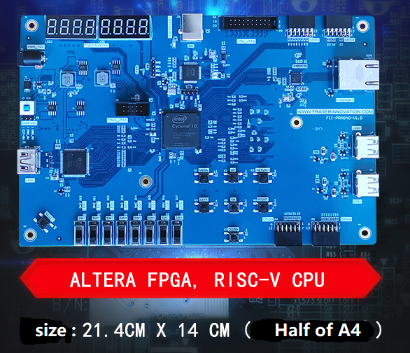
- Size : 21.4cm x 14 cm (Half A4 )
Official Shopping Website:
https://fpgamarketing.com/FII-PRA040-Altera-risc-v-Cyclone10-FPGA-Boards-FII-PRA040.htm?


Altera Xilinix RISC-V SoC AI FII-PRA040 Educational Platform – Side View
We will send you following documents after you have bought our products:
PRA040 Hareware Configuration Reference Guide
PRA040 Schematic Diagram
Altera Risc-V User Experimental Manual – PRA040
- Altera Risc-V FPGA Board Tutorial : Introduction of FII-PRA040 Development System
- Altera Risc-V FPGA Tutorial : LED shifting – FII-PRA040 FPGA Board Experimental 1
- Altera Risc-V FPGA Tutorial : SignalTap – FII-PRA040 FPGA Board Experimental 2
- Altera Risc-V FPGA Tutorial : Segment Display – FII-PRA040 FPGA Board Experimental 3
- Altera Risc-V FPGA Tutorial : Block/SCH – FII-PRA040 FPGA Board Experimental 4
- Altera Risc-V FPGA Tutorial : Button Debounce – FII-PRA040 FPGA Board Experimental 5
- Altera Risc-V FPGA Tutorial : Use of Multipliers and ModelSim – FII-PRA040 FPGA Board Experimental 6
- Altera Risc-V FPGA Tutorial : Hexadecimal Number to BCD Code Conversion and Application – FII-PRA040 FPGA Board Experimental 7
- Altera Risc-V FPGA Tutorial : Use of ROM – FII-PRA040 FPGA Board Experimental 8
- Altera Risc-V FPGA Tutorial : Use Dual-port RAM to Read and Write Frame Data – FII-PRA040 FPGA Board Experimental 9
- Altera Risc-V FPGA Tutorial :Asynchronous Serial Port Design and Experiment – FII-PRA040 FPGA Board Experimental 10
- Altera Risc-V FPGA Tutorial : IIC Protocol Transmission – FII-PRA040 FPGA Board Experimental 11
- Altera Risc-V FPGA Tutorial :AD,DA Experiment – FII-PRA040 FPGA Board Experimental 12
- Learn HDMI principle, Introduction to HDMI and ADV7511 Chip, HDMI Display, FII-PRA040 Altera Risc-V tutorial Experiment 13
- How does Ethernet work? MII, GMII, RGMII interface advantages and disadvantages, Perform a loopback test, FII-PRA040 Altera Risc-V Tutorial Experiment 14
- How does SRAM read and write work ? Review frequency division, button debounce, and hex conversion experiment – FII-PRA040 Altera Risc-V Tutorial Experiment 15
- Audio 8978 Loopback Experiment (WM8978 Audio Sub Development Board) , How I2S (Inter-IC Sound) bus work ? – – FII-PRA040 Altera Risc-V Tutorial Experiment 16
- OV5640 Camera Photo Display Experiment, IIC bus, HDMI, Understand the power-on sequence of the OV5640 – FII-PRA040 Altera Risc-V Experiment 17
- High-speed ADC9226 Acquisition Experiment (FII-BD9226) – parallel ADC collectors and master the use of ADC9226 – FII-PRA040 Altera Risc-V Experiment 18
- DAC9767 DDS Signal Source Experiment, AD9767 datasheet and use the AD9767 to design a signal source that can generate sine, square, triangle, and sawtooth waves – FII-PRA040 Altera Risc-V Experiment 19
More Information about PRA040 Altera Risc-V FPGA Board.
1、Design Objective of the System
The main purpose of this system design is to complete FPGA learning, development and experiment with Intel Quartus. The main device uses the Inte Cyclone10 10CL040YF484C8G and is currently the latest generation of FPGA devices from Intel. The major learning and development projects can be completed as follows:
- Basic FPGA design training
- Construction and training of the SOPC (NiosII) system
- IC design and verification, the system provides hardware design, simulation and verification of RISC-V CPU
- Development and application based on RISC-V
- The system is specifically optimized for hardware design for RISC-V system applications
2、System Resource
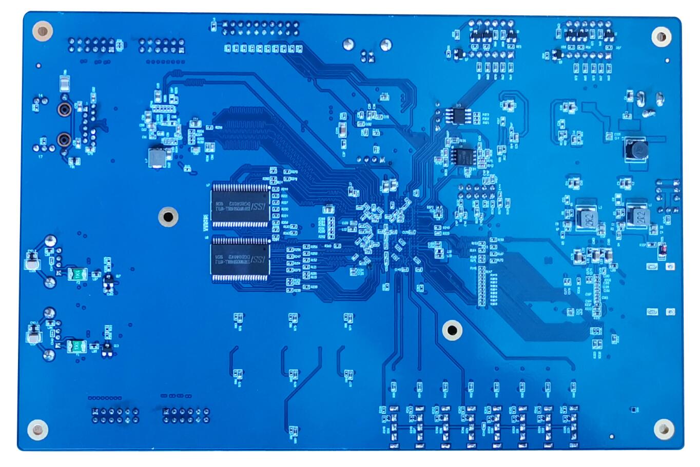
- Extended memory: Two Super Sram (IS61WV51216, 512K x 32bit) are connected in parallel to form a 32-bit data interface, and the maximum access space is up to 2M bytes.
- Serial flash: Spi interface serial flash (16M bytes)
- Serial EEPROM
- Gigabit Ethernet: 100/1000 Mbps
- USB to serial interface: USB-UART bridge
3、Human-computer Interaction Interface
- 8 DIP switches
- 8 push buttons, definition of 7 push buttons: MENU, UP, RETUN, LEFT, OK, RIGHT, DOWN, 1 for reset: RESET
- 8 LEDs
- 6 7-segment LED display
- I2C bus interface
- UART external interface
- Two JTAG programming interfaces: One is for downloading the FPGA debug interface, and the other is the JTAG debug interface for RISC-V CPU
- Built-in RISC-V CPU software debugger, no external RISC-V JTAG emulator required
- 4 12-pin GPIO connectors, in line with PMOD interface standards
4、Software Development System
- Quartus 18.0 and later version for FPGA development, Nios-II SOPC
- Freedom Studio-Win_x86_64 software development for RISC-V CPU
5、Supporting Resources
RISC-V JTAG Debugger Intel Altera JTAG Download Debugger FII-PRA040 User Experimental Manual FII-PRA040 Hardware Reference Guide
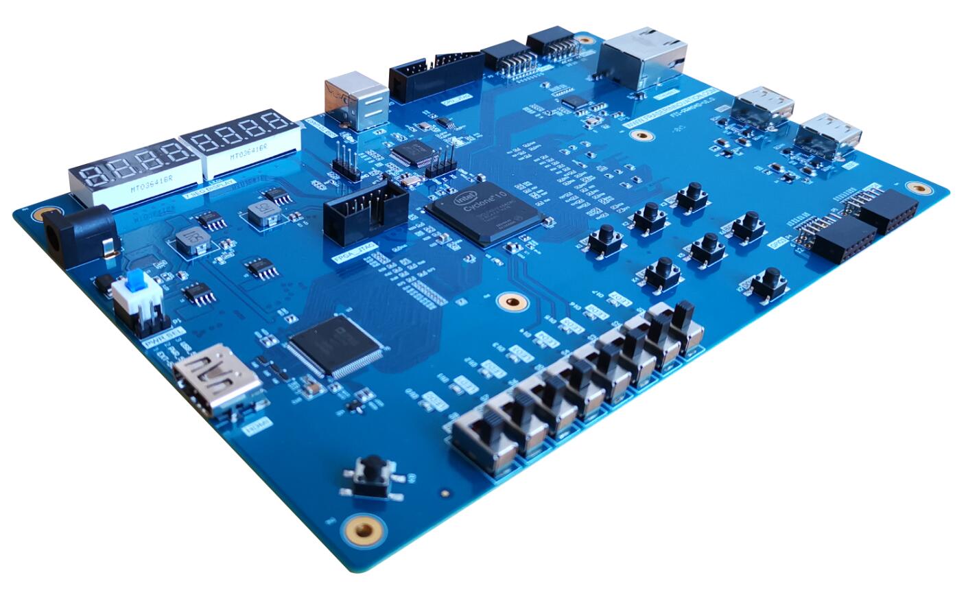
6、Physical Picture
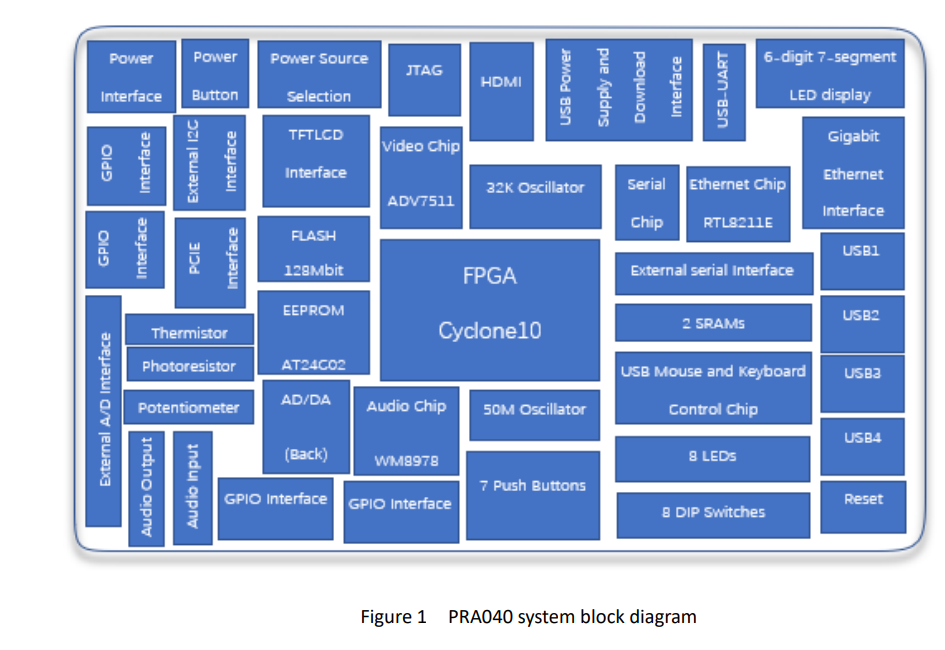
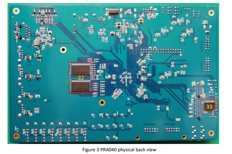
Corresponding to the physical picture, the main devices on board are as follows:
1、10CL040YE484C8G chip
2、External 12V power interface
3、GPIO interface
4、Thermistor (NTC-MF52)
5、Photoresistor
6、Potentiometer
7、Audio output (green), audio input (red)
8、PCIE interface
9、TFTCLD interface
10、Audio chip (WM8978)
11、7 push buttons
12、50M system clock
14、Video chip(ADV7511)
15、External JTAG download interface
16、HDMI interface
17、USB power supply and download interface
18、FPGA and RISC_V JTAG download chips (FT2232)
19、USB_UART interface
20、Serial chip (CP2102)
21、6 7-segment LED display
22、Ethernet interface
23、Ethernet PHY chip (RTL8211E-VB)
24、4 USB interfaces
25、USB mouse and keyboard control chip
26、8 LEDs
27、8-bit DIP switch
28、Reset button
29、Power button
30、Flash (N25Q128A,128M bit/16M bytes)
31、EEPROM (AT24C02N)
32、Two SRAMs
33、AD/DA conversion chip (PCF8591)
Reviews
There are no reviews yet.