
JTAG (named after the Joint Test Action Group which codified it) is an industry standard for verifying designs and testing printed circuit boards after manufacture.
Buy ALTERA, RISC-V, ARM CORTEX FPGA JTAG
FPGA Study Board, Verilog and VHDL for beginner
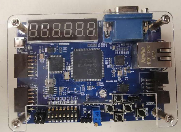
– Cyclone-10 FPGA Development Board with Jtag Embeded – FII-PRA010 – $59

For more FPGA board for beginner information, please check here
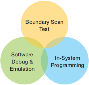
Processors often use JTAG to provide access to their debug/emulation functions and all FPGAs and CPLDs use JTAG to provide access to their programming functions.
JTAG implements standards for on-chip instrumentation in electronic design automation (EDA) as a complementary tool to digital simulation. It specifies the use of a dedicated debug port implementing a serial communications interface for low-overhead access without requiring direct external access to the system address and data buses.
The interface connects to an on-chip test access port (TAP) that implements a stateful protocol to access a set of test registers that present chip logic levels and device capabilities of various parts.
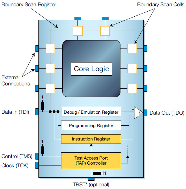
Figure 1 – Schematic Diagram of a JTAG enabled device
The JTAG standards have been extended by many semiconductor chip manufacturers with specialized variants to provide vendor-specific features.
The debug and programming tools commonly associated with JTAG only make use of one aspect of the underlying technology – the four-wire JTAG communications protocol.
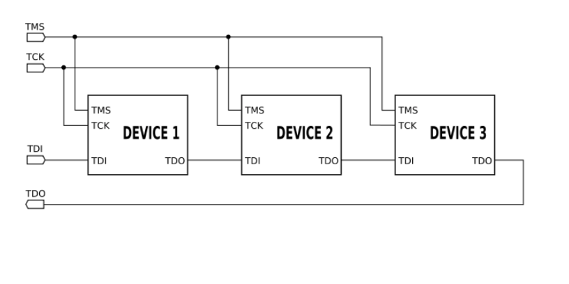
These four signals, collectively known as the Test Access Port or TAP, are part of IEEE Std. 1149.1. This standard was developed to provide a technology for testing Printed Circuit Board Assemblies (PCBAs) without needing the level of physical access required for bed-of-nails testing or the amount of custom development needed for functional test. The TAP was designed to interact with new registers that were added to devices to implement this method of testing.
Very quickly however silicon manufacturers recognised the benefits of using the TAP to access registers offering other functionalities such as debug and programming.
The main register added to a device specifically for JTAG testing is called the Boundary Scan Register (BSR). As its name suggests the individual bits, or cells, of this register are at the boundary of the device, between its functional core and the pins or balls by which it is connected to a board – very often JTAG testing is referred to as boundary scan.
The process of boundary scan can be most easily understood with reference to the schematic diagram shown in figure 1.
All the signals between the device’s core logic and the pins are intercepted by a serial scan path known as the Boundary Scan Register (BSR) which consists of a number of boundary scan ‘cells’. In normal operation these boundary scan cells are invisible. However, in test mode the cells can be used to set and/or read values from the device pins (or in ‘internal’ mode from values of the core logic.) Not all boundary scan cells are the same – there are 10 types of cell in the 1149.1 standards, though manufacturers can define non-standard cell types to match the actual hardware functionality of their device if they wish.
Interface Signals
The JTAG interface, collectively known as a Test Access Port, or TAP, uses the following signals to support the operation of boundary scan.
- TCK (Test Clock) – this signal synchronizes the internal state machine operations.
- TMS (Test Mode Select) – this signal is sampled at the rising edge of TCK to determine the next state.
- TDI (Test Data In) – this signal represents the data shifted into the device’s test or programming logic. It is sampled at the rising edge of TCK when the internal state machine is in the correct state.
- TDO (Test Data Out) – this signal represents the data shifted out of the device’s test or programming logic and is valid on the falling edge of TCK when the internal state machine is in the correct state.
- TRST (Test Reset) – this is an optional pin which, when available, can reset the TAP controller’s state machine.
Registers
There are two types of registers associated with boundary scan. Each compliant device has one instruction register and two or more data registers.
Instruction Register – the instruction register holds the current instruction. Its content is used by the TAP controller to decide what to do with signals that are received. Most commonly, the content of the instruction register will define to which of the data registers signals should be passed.
Data Registers – there are three primary data registers, the Boundary Scan Register (BSR), the BYPASS register and the IDCODES register. Other data registers may be present, but they are not required as part of the JTAG standard.
- BSR – this is the main testing data register. It is used to move data to and from the I/O pins of a device.
- BYPASS – this is a single-bit register that passes information from TDI to TDO. It allows other devices in a circuit to be tested with minimal overhead.
- IDCODES – this register contains the ID code and revision number for the device. This information allows the device to be linked to its Boundary Scan Description Language (BSDL) file. The file contains details of the Boundary Scan configuration for the device.
How JTAG / boundary scan is used to test a board
Boundary scan cells (see above) can operate in two modes. In their functional mode they have no effect on the operation of the device – this is the mode in which they operate when the board is running normally. In their test mode they disconnect the functional core of the device from the pins. By putting boundary scan cells into test mode they can be used to control the values being driven from an enabled device onto a net and also be used to monitor the value of that net.
Disconnecting the control of the pins from the functionality of the enabled device makes boundary scan test development significantly easier than traditional functional test as no device configuration or booting is required to use the pins. By providing a mechanism to control and monitor all the enabled signals on a device from a four-pin TAP, JTAG significantly reduces the physical access required to test a board.
There are two main ways that this boundary scan capability can be used to test a board. The first way, connection testing (see next section) gives good test coverage, particularly for short circuit faults. It is based purely on the JTAG device capabilities, the connections and nets on the board and – in the case of XJTAG – the logic functionality on a board. The second way extends this coverage by using the JTAG enabled devices on a board to communicate with non-JTAG peripheral devices such as DDR RAM and flash.
What is a JTAG connection test?
A JTAG connection test will check that the connections around the JTAG enabled devices on a board are the same as those specified in the design.
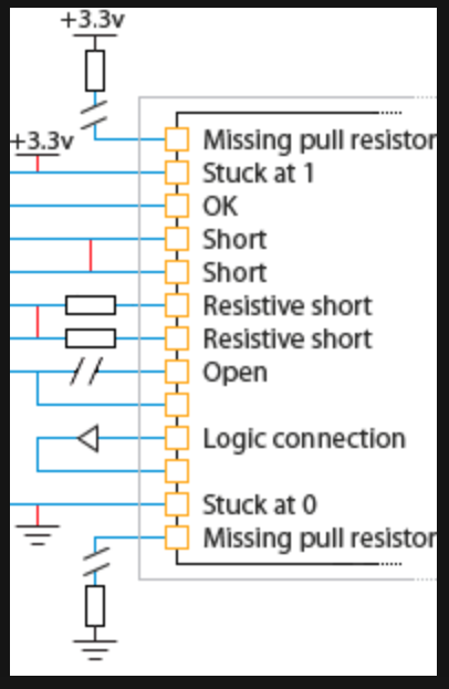
Where two JTAG enabled pins are meant to be connected the test will make sure one pin can be controlled by the other. Where enabled pins are not meant to be connected they are tested for short circuit faults by driving one pin and checking that these values are not read on the other pins.
Missing pull resistors and ‘stuck-at’ faults can also be found by a connection test as well as faults involving logic devices whose behaviour can be described in a truth table.
XJTAG will automatically generate the vectors required to run a connection test based on the netlist of a board and JTAG information for the enabled devices.
What about devices that are not JTAG enabled?
While the main devices, such as processors and FPGAs, are normally JTAG enabled, there will be many devices in every design that are not. DDR, SDRAM, SRAM, flash, MDIO controlled Ethernet PHYs, SPI and I2C temperature sensors, real time clocks, ADCs and DACs are just some examples of such devices.
The connection test will still provide excellent coverage for short circuit faults on the nets linking these non-JTAG devices to JTAG enabled devices; however it cannot check for open circuit faults at either the JTAG device or the non-JTAG device.
In order to add this open circuit coverage it is necessary to communicate with the peripheral device from boundary scan on the enabled device. If communication can be verified, there cannot be an open circuit fault. This type of testing can be very simple, for example lighting an LED and asking an operator to verify it has activated, or more complex, for example writing data into the memory array of a RAM and reading it back.
Is it a lot of work to create a JTAG test system?
Using the libraries for standard non-JTAG components provided by XJTAG, you can get a set of tests up and running for your board with no code development. The library files contain models for all types of non-JTAG devices from simple resistors and buffers to complex memory devices such as DDR3. Because boundary scan disconnects the control of the pins on JTAG devices from their functionality the same model can be used irrespective of the JTAG device controlling a peripheral.
Most boards already contain JTAG headers for programming or debug so there are no extra design requirements.
Where do I get information about the JTAG in my devices?
In order to run any boundary scan based testing it is necessary to have some information about the implementation of JTAG on the enabled devices on a board. This information comes from the BSDL (Boundary Scan Description Language) files for these devices. BSDL files must be made available by the silicon vendor for a device to be compliant with IEEE Std. 1149.1.
Is JTAG test just used in production?
Not at all. One of the key benefits to boundary scan testing is that the only test hardware required is a JTAG controller. Other production test technologies such as flying probe, automated optical/X-ray inspection or bed-of-nails all require specialised test equipment that will not be available on an engineer’s bench.
Using boundary scan during board bring-up can remove uncertainties – hardware engineers can test prototype boards for manufacturing defects before system testing, and even before firmware is complete. Test systems developed at this early stage of the product lifecycle can easily be reused, and extended for production.
Test Access Port (TAP) Controller
The TAP controller, a state machine whose transitions are controlled by the TMS signal, controls the behaviour of the JTAG system. Figure 2, below, shows the state-transition diagram.
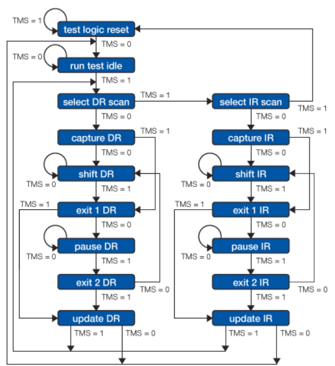
TAP State machine
All states have two exits, so all transitions can be controlled by the single TMS signal sampled on TCK. The two main paths allow for setting or retrieving information from either a data register or the instruction register of the device. The data register operated on (e.g. BSR, IDCODES, BYPASS) depends on the value loaded into the instruction register.
For more detail on each state, refer to the IEEE 1149.1 Standard JTAG document.
Boundary Scan Instructions
The IEEE 1149.1 standard defines a set of instructions that must be available for a device to be considered compliant. These instructions are:
- BYPASS – this instruction causes the TDI and TDO lines to be connected via a single-bit pass-through register (the BYPASS register). This instruction allows the testing of other devices in the JTAG chain without any unnecessary overhead.
- EXTEST – this instruction causes the TDI and TDO to be connected to the Boundary Scan Register (BSR). The device’s pin states are sampled with the ‘capture dr’ JTAG state and new values are shifted into the BSR with the ‘shift dr’ state; these values are then applied to the pins of the device using the ‘update dr’ state.
- SAMPLE/PRELOAD – this instruction causes the TDI and TDO to be connected to the BSR. However, the device is left in its normal functional mode. During this instruction, the BSR can be accessed by a data scan operation to take a sample of the functional data entering and leaving the device. The instruction is also used to preload test data into the BSR prior to loading an EXTEST instruction.
Other commonly available instructions include:
- IDCODE – this instruction causes the TDI and TDO to be connected to the IDCODE register.
- INTEST – this instruction causes the TDI and TDO lines to be connected to the Boundary Scan Register (BSR). While the EXTEST instruction allows the user to set and read pin states, the INTEST instruction relates to the core-logic signals of a device.
Obtaining the IEEE 1149.1 Standard
The IEEE 1149.1 Standard JTAG specification is available directly from IEEE:
JTAG facilities
This debug TAP exposes several standard instructions, and a few specifically designed for hardware-assisted debugging, where a software tool (the “debugger”) uses JTAG to communicate with a system being debugged:
BYPASS and IDCODE, standard instructions as described above
EXTEST, INTEST, standard instructions, but operating on the core instead of an external boundary scan chain. EXTEST is nominally for writing data to the core, INTEST is nominally for reading it; but two scan chains are exceptions to that rule.
SCAN_N ARM instruction to select the numbered scan chain used with EXTEST or INTEST. There are six scan chains:
- 0 – Device ID Register, 40 bits of read-only identification data
- 1 – Debug Status and Control Register (DSCR), 32 bits used to operate the debug facilities
- 4 – Instruction Transfer Register (ITR), 33 bits (32 instruction plus one status bit) used to execute processor instructions while in a special “Debug Mode” (see below)
- 5 – Debug Communications Channel (DCC), 34 bits (one long data word plus two status bits) used for bidirectional data transfer to the core. This is used both in debug mode, and possibly at runtime when talking to debugger-aware software.
- 6 – Embedded Trace Module (ETM), 40 bits (7 bit address, one 32-bit long data word, and a R/W bit) used to control the operation of a passive instruction and data trace mechanism. This feeds either an on-chip Embedded Trace Buffer (ETB), or an external high speed trace data collection pod. Tracing supports passive debugging (examining execution history) and profiling for performance tuning.
- 7 – debug module, 40 bits (7 bit address, one 32-bit long data word, and a R/W bit) used to access hardware breakpoints, watchpoints, and more. These can be written while the processor is running; it does not need to be in Debug Mode.
HALT and RESTART, ARM11-specific instructions to halt and restart the CPU. Halting it puts the core into the “Debug Mode”, where the ITR can be used to execute instructions, including using the DCC to transfer data between the debug (JTAG) host and the CPU.

ITRSEL, ARM11-specific instruction to accelerate some operations with ITR.
That model resembles the model used in other ARM cores. Non-ARM systems generally have similar capabilities, perhaps implemented using the Nexus protocols on top of JTAG, or other vendor-specific schemes.
Older ARM7 and ARM9 cores include an EmbeddedICE module which combines most of those facilities, but has an awkward mechanism for instruction execution: the debugger must drive the CPU instruction pipeline, clock by clock, and directly access the data buses to read and write data to the CPU. The ARM11 uses the same model for trace support (ETM, ETB) as those older cores.
JTAG, JTAG facilities, JTAG programmer, JTAG connector
Newer ARM Cortex cores closely resemble this debug model, but build on a Debug Access Port (DAP) instead of direct CPU access. In this architecture (named CoreSight Technology), core and JTAG module is completely independent.
They are also decoupled from JTAG so they can be hosted over ARM’s two-wire SWD interface (see below) instead of just the six-wire JTAG interface. (ARM takes the four standard JTAG signals and adds the optional TRST, plus the RTCK signal used for adaptive clocking.)
The CoreSight JTAG-DP is asynchronous to the core clocks, and does not implement RTCK. Also, the newer cores have updated trace support.
You can buy JTAG online in FPGAMarketing.com website and chose from eight different JTAG connector and JTAG Programmer.