zynq xc7z030 board – FII-PE7030 Experiment 4 -Digital clocl comprehensive design result
FII-PE7030 FPGA Board Based FPGA Products

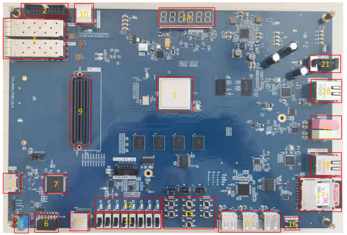
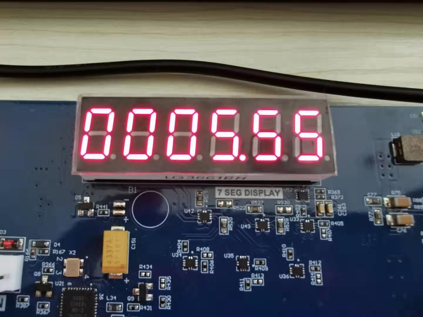
zynq xc7z030 board – FII-PE7030 Experiment 5 – Digital Clock Comprehensive Experiment

Experiment 5 Digital Clock Comprehensive Experiment 5.1 Experiment Objective Review the segment display content of experiment 3, and the button debounce content of experiment 4; Combine experiment 3 and experiment 4 to design a complete adjustable digital clock; 5.2 Experiment Implement Set four push buttons (left, right, up, down); Left and right push buttons control the calibration function, switch between segment display of hour, minute and second; Up and down calibration by adding 1 and subtracting 1 to the data to be calibrated; Modular design so that the design can…

Read More
FII-PE7030-Physical-Picture
FII-PE7030 FPGA Products

zynq_7030 Main Resources Usage and FPGA Development Experiemnt

This part mainly guides the user to learn the development of FPGA program and the use of onboard hardware through the development example of FPGA. At the same time, the application system software Xilinx is introduced from the elementary to the profound. The development exercises covered in this section are as follows: Experiment 1: LED shifting design Experiment 2: ILA experiment Experiment 3: Segment display digital clock experiment Experiment 4: button debouncing experiment Experiment 5: digital clock comprehensive experiment Experiment 6: use of multiplier and ISIM simulation Experiment 7: hex…

Read More