
Description
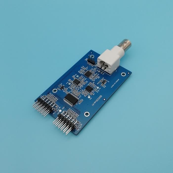
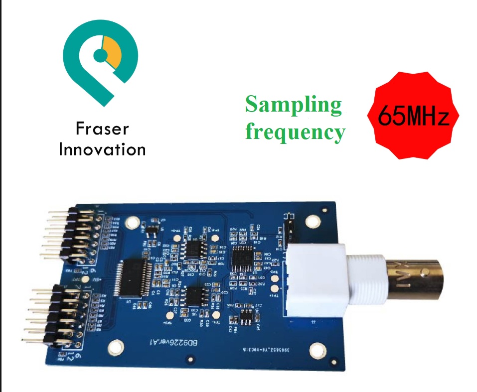
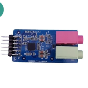
High speed AD module -12 Digital – 65MHz Data Sampling Digital analog signal development board BNC- AD9226 – FII-BD9226
Product Features:
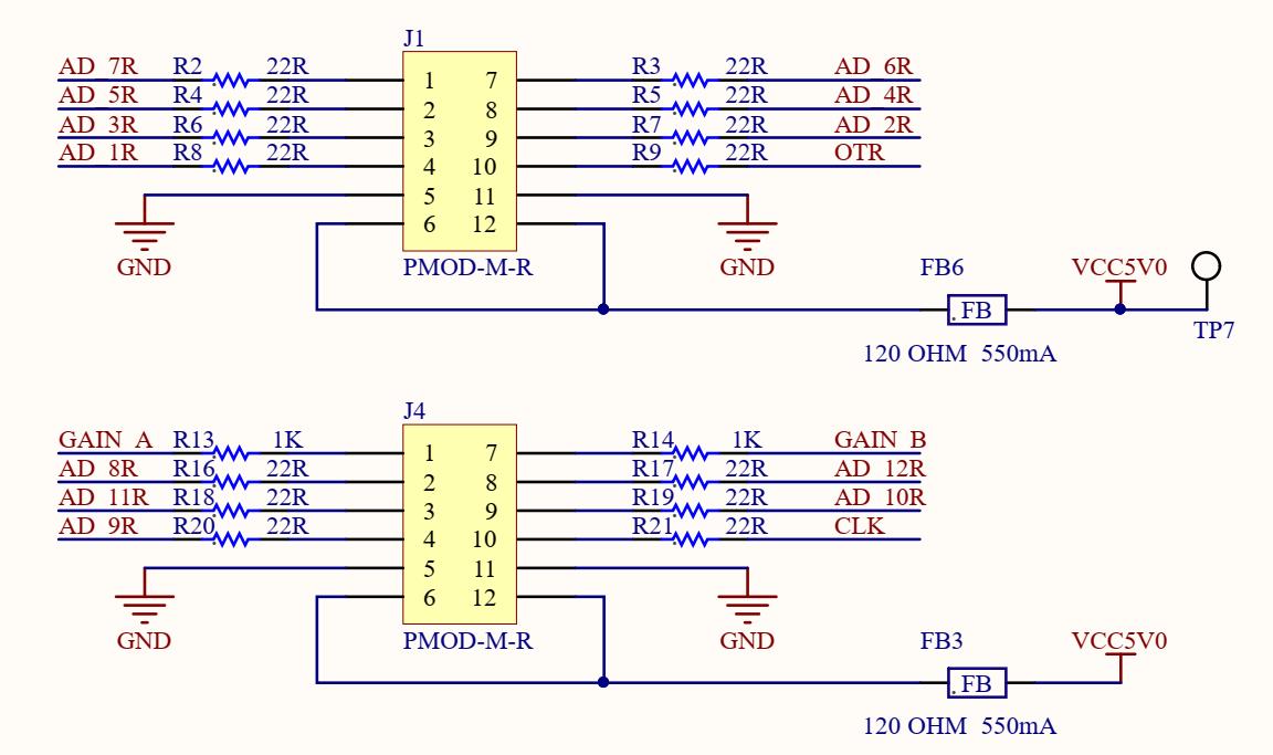
Digital interface:Standard PMOD Interface,work with any fpga board that has PMOD interface;
Analog interface:BNC Interface output;
Number of channels: single channel;
AD Conversion Chip:AD9226 Chip;
DA Number of conversion bits:12bit;
Maximum sampling rate: 65MSPS;
Analog signal input amplitude: ±5V (peak-to-peak 10V)
Module power supply: +5V single power supply;
Test points: up to 7 test points;
Operating temperature: -40 ° C ~ 85 ° C, to meet the industrial temperature range;
Provide information and DDS case code;
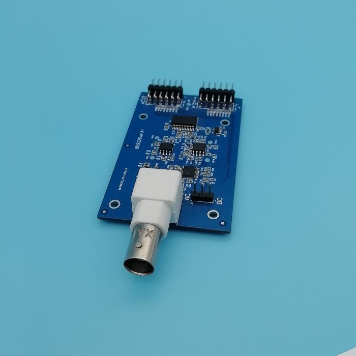
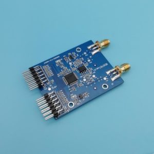
Interface Defination
More information about this board:
What is the input impedance? The recommended input impedance is 50ohm.
What is the bandwidth? The analog input bandwidth is 750MHz.
What is the input voltage range? The recommend power supply is 5V, and IO voltage is 3.3V.
This this board uses multiple PMOD connectors, can you tell me the distance between them (pin 1 to pin 1 distance)? I want to know if it will fit into Digilent Arty-7 boards.
The pin1 to pin1 distance is 880mil(22.352mm), it will fit into Digilent Arty-7 boards.
I want to know the distance between the PMOD plugs (will it fit in the Digilent Arty-7 board)?
Also what impedance is the input? What bandwidth can I expect?
High-speed ADC9226 Acquisition Experiment (FII-BD9226) Experiment:
Experiment 18 High-speed ADC9226 Acquisition Experiment
18.1 Experiment Objective
Learn about parallel ADC collectors and master the use of ADC9226.
18.2 Experiment Implement
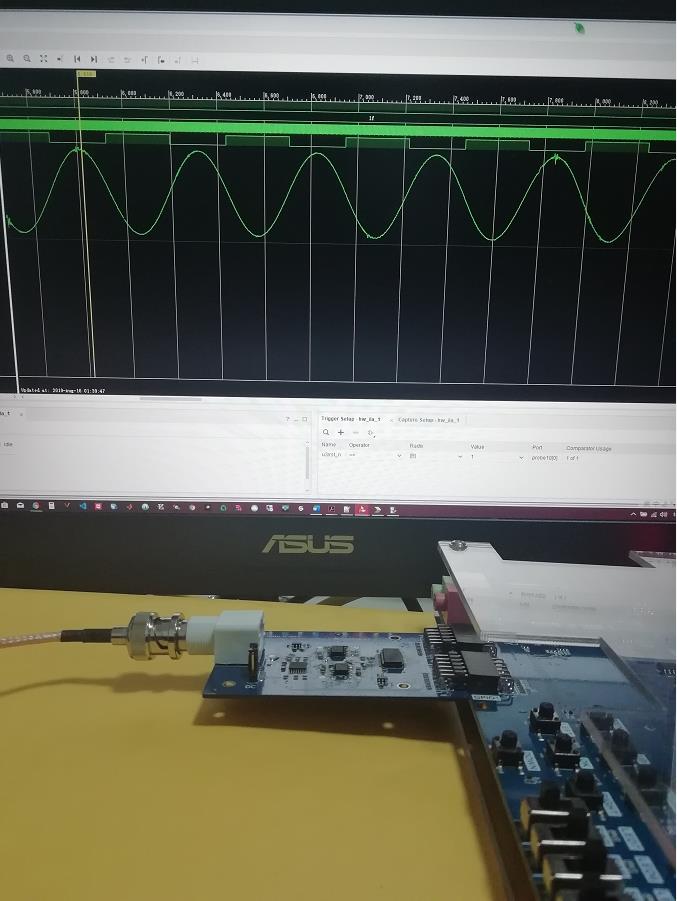
Insert the ADC9226 module face up into the FPGA development board to the GPIO2 and GPIO1 ports which are next to the red-green audio module. Write programs to use this module to test
18.3 Experiment
18.3.1 ADC9226 Module Introduction
ADC9226 module adopts AD9226 chip design of ADI Company. This chip is a monolithic, 12-bit, 65 MSPS analog-to-digital converter (ADC). It uses a single power supply and has an on-chip high-performance sample-and-hold amplifier and voltage reference. It uses a multistage differential pipelined architecture with a data rate of 65 MSPS and guarantees no missing codes over the full operating temperature range.
See Figure 18.1 for ADC9226 timing diagram.

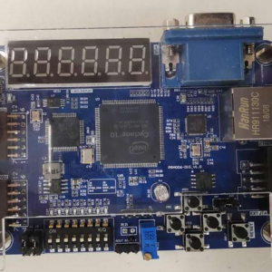
FPGA development board
Figure18.1 ADC9226 timing diagram
From this timing diagram, we know that there is no need to configure the AD9226 chip, as long as the appropriate CLOCK is provided, the chip can perform data acquisition.
18.3.2 Program Design
For more information, please check Altera Risc-V FII-PRA040 experiment 18.
If you have any questions, you can contact us or post in the Sub-Board product forums. If you can not register to post, please let us know and I will create a forum username for you.
Reviews
There are no reviews yet.