
A printed circuit board (PCB) mechanically supports and electrically connects electrical or electronic components using conductive tracks, pads and other features etched from one or more sheet layers of copper laminated onto and/or between sheet layers of a non-conductive substrate. Components are generally soldered onto the PCB to both electrically connect and mechanically fasten them to it.
PCB is a key interconnection for assembling electronic parts. It is a necessary equipment for most electronic equipment and products. So it is also called “the mother of electric products”. We can see PCB products everywhere: mobile phones, tablets, air conditioners, refrigerators, etc. almost cover your entire life.
Printed circuit boards are used in all but the simplest electronic products. They are also used in some electrical products, such as passive switch boxes.

With the advent of the 5G era, many aspects of our society will be changing. Just as 4G has spawned short videos and video calls and changed people’s ways of social entertainment, what changes will 5G bring to us?
In the 5G era, VR/AR, smart home, smart city, etc., smart life makes the application of electronic products more extensive, and the development of PCB will inevitably enter a new height.

After years of research and practice, Fraser Innovation Inc PCB design team can well meet any requirements of high-speed PCB design.
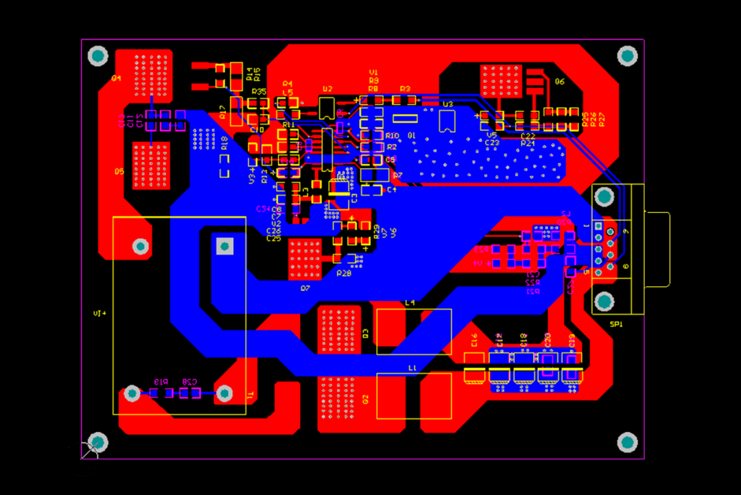
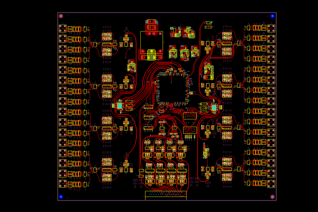
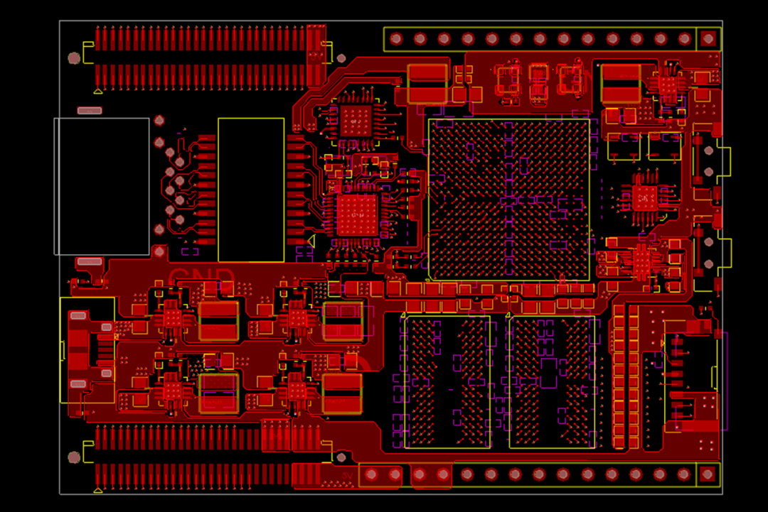
We can provide you with high-quality, fast speed electronic, communication products such as high-speed, high-density, mixed digital and analog PCB design. We can also provide new PCB layout design (such as flexible boards, HDI, buried blind holes, etc.) and other services.
We have a group of high-quality PCB design engineers who have rich experience in the design of carrier-grade high-speed multilayer PCBs. Our team of engineers and CAD/CAM operators are available to discuss any project needs that our customer may have as we are fully licensed and utilize industry leading tools, including Cadence Allegro, Mentor Expedition, Mentor’s PADS, Altium, Valor for DFM Analysis.
Our Capabilities Encompass The Full Design Flow From Start To Finish Including:
- Micro BGA / Micro Via / Blind and Buried Vias
- Stripline, Microstrip, Signal matching solutions, and Signal quality
- Signal Routing Topology
- Power Source Decoupling
- High-speed Signal Current Return
- Path Signal Impedance Control
- Multilayer Stackup Control
- Single Board EMC/EMI Strategy Analysis
- Buried Blind Hole Blind VIA and Buried VIA
- Rules Driven Designs
- Schematic Capture
- Library Development
- Database Construction and Verification
- Signal Integrity/Design Verification
- EMI Checking
- Full Document Package Creation
PCB Layout and Design from us


In the design, we will weigh various factors and make a comprehensive compromise: not only meet the requirements of high-speed PCB design, but also reduce the complexity of the design.
Our adoption of high-speed PCB design methods constitutes the controllability of the design process. Only controllable PCB Layout and Design are reliable, and successful design.
Professional technical team, first-class service quality, strong after-sales service, dedicated person responsible for project progress tracking and feedback, use strength to do every product, and serve every customer attentively, we have all the staff in place, ready to test you Welcome your inquiry.
Canada Headquarters
Fraser Innovation Inc.
103-11951 Hammersmith Way
Richmond, BC V7A 5H9 Canada
Tel: 1 604 3703096