zynq xc7z030 board – use Vivado to establish a new project, call the system resource PLL to establish the clock, Write Verilog HDL program to achieve frequency division and implement LED shifting,FII-PE7030 Experiment 1 LED Shifting Design
Experiment 1 LED Shifting Design
1.1 Experiment Objective
- Practice how to use the development system software Vivado to establish a new project, call the system resource PLL to establish the clock.
- Write Verilog HDL program to achieve frequency division and implement LED shifting
- Combine hardware resources for FPGA pin configuration
- Compile, download the program to the develop board, and verify
- Observe the experimental result and debug the project
1.2 Experiment Implement
- All LEDs light up during reset;
- After reset, LED lights from low to high (from right to left) in turn;
- Each LED is lit for one second;
- After the last (highest position) LED is lit, the next time it returns to the first (lowest position) LED, the loop is achieved;
1.3 Experiment
1.3.1 LED Introduction
LED (Light-Emitting Diode), is characterized by low operating current, high reliability and long life. Up to now, there are many types of LED lights, as shown in Figure 1.1. The FII-PE7030 uses the LED lights in the red circle.
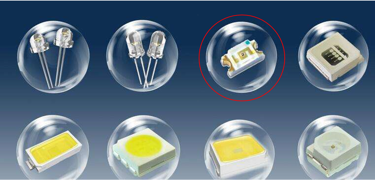
Figure 1.1 Different kinds of LEDs
1.3.2 Hardware Design
The physical picture of the onboard 8-bit LED is shown in Figure 1.2. The schematics of LED is shown in Figure 1.3. The LED module of this experiment board adopts 8 common anode LEDs, which are connected with Vcc 5V through 510 R resistors, and the negative electrode is grounded through the N-channel field effect transistor (FET), the gate of the FET is grounded through a 4.7K resistor, and the FPGA is connected to the gate of the FET through the GPIO_DIP_SW terminal.When the FPGA outputs a high level of 1, a current flows through the LED, and it is turned on.
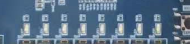
Figure 1.2 8-bit LED physical picture
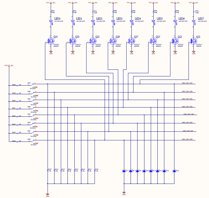
Figure 1.3 Schematics of LED
1.3.3 Program Design
1.3.3.1 Start Program
Before writing a program, let’s briefly introduce the development environment we use and how to create a project. Take Vivado 18.2 as an example. The specific project establishment steps are shown in Figure 1.4 to 1.9.
The first step: open the Vivado 2018.2 integrated development environment
Figure 1.4 Vivado development environment
The secodn step: under the Quick Start group in the main interface of the Vivado 2018.2, click the Create Project option to bring up the Create a New Vivado Project dialog box. Click Next to bring up the Project Name dialog box. In Figure 1.5, determine the project name and project location. Take this experiment as an example, set the parameters according to the figure.
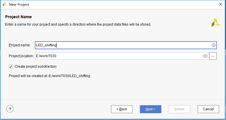
Figure 1.5 New Project-Project Name dialog box
The third step: click the Next button in Figure 1.5 to bring up the Project Type dialog box, as shown in Figure 1.6.
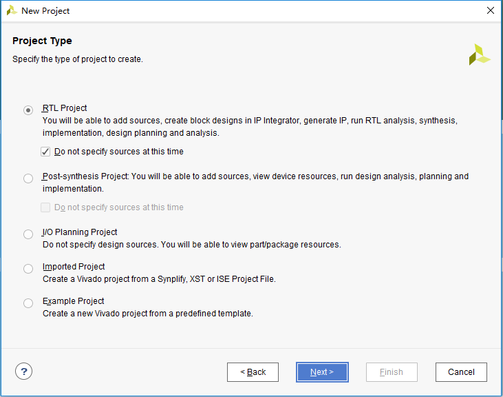
Figure 1.6 New Project-Project Type dialog box
- Choose RTL Project
- Check Do not specify sources at this time
The fourth step: click the Next button in Figure 1.6 to bring up the Default Part dialog.
In order to speed up the search for the device, as shown in Figure 1.7, set the parameters according to the figure.
- Category:ALL
- Family:Zynq_7000
- Package:ffg676
- Speed:-1
- Temperature:All Remaining
The window shown in Figure 1.7 lists the devices available for selection. In this design, the device model number is xc7z030ffg676-1.
The fifth step: click the Next button in Figure 1.7 to bring up the New Project Summary dialog box, as shown in Figure 1.8. This dialog box explains the type, name, and device information of the new project.
The sixth step: click the Finish button in Figure 1.8 to complete the creation of the new project.
After the creation is successful, Vivado automatically transfers to the PROJECT MANAGER interface, as shown in Figure 1.9, for developers to proceed to the next step.
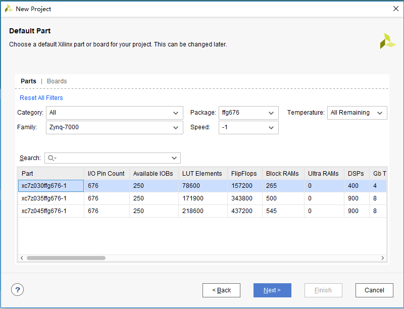
Figure 1.7 Default Part dialog box
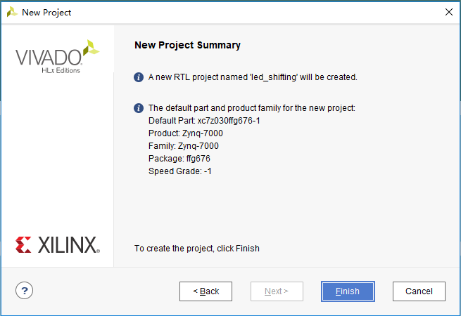
Figure 1.8 New Project Summary dialog box
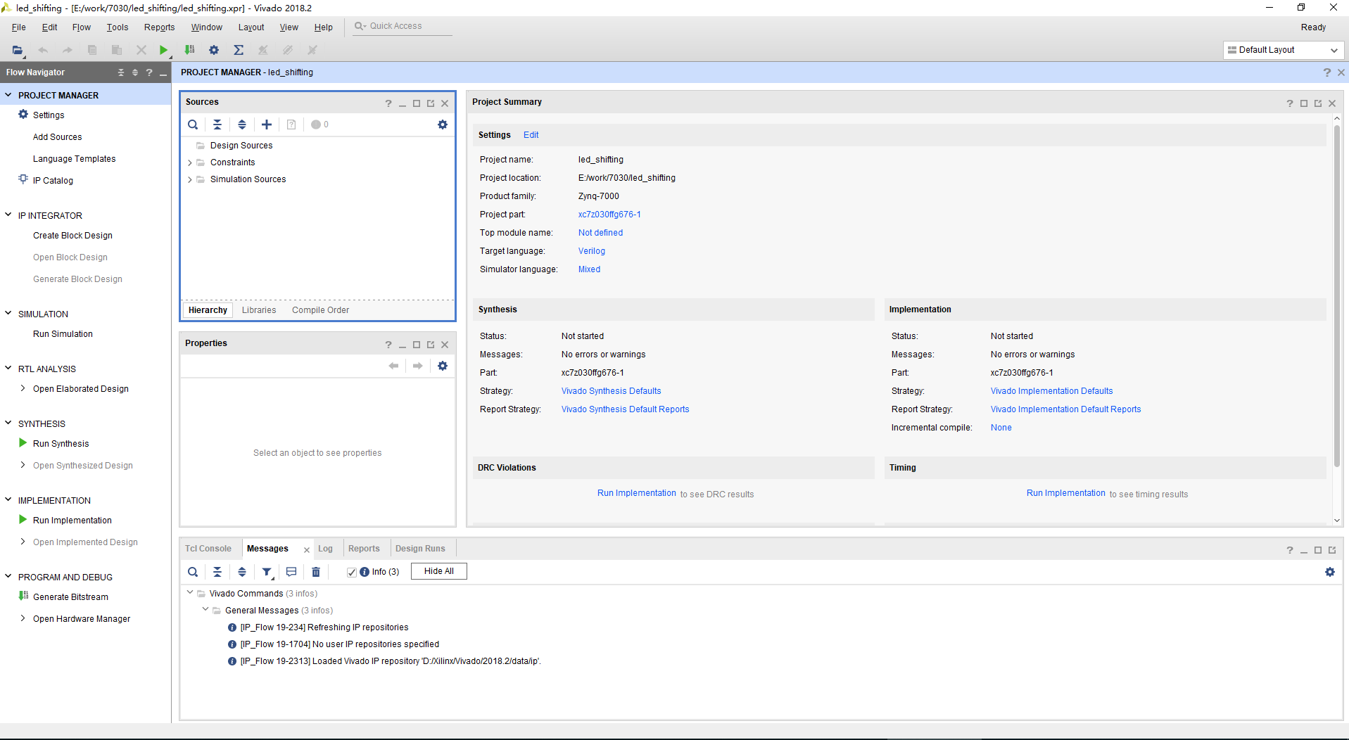
Figure 1.9 PROJECT MANAGER interface
1.3.3.2 Create and Add a New Design File
After the new project is created, continue to create the file (Verilog HDL file). The steps are as follows.
The first step: select the Design Sources folder under the Sources window, click the icon ╋ in the window, or click the right mouse button to bring up the floating menu, execute the Add Sources command, and Add Sources dialog box pops up. As shown in Figure 1.10, select Add or create design sources.
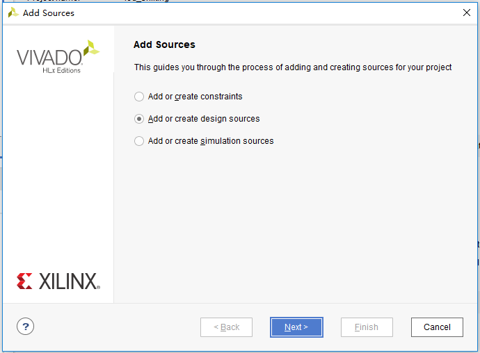
Figure 1.10 Add Sources dialog box
The second step: click the Next button in Figure 1.10 to bring up the Add or Create Design Sources dialog box, as shown in Figure 1.11.
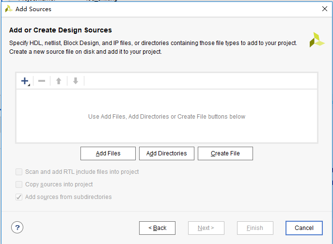
Figure 1.11 Add or Create Design Sources dialog box
The third step: click the Create File button in Figure 1.11; or click the icon ╋, the floating menu appears, select the Create File.
The fourth step: the Create Source File dialog box pops up, as shown in Figure 1.12.
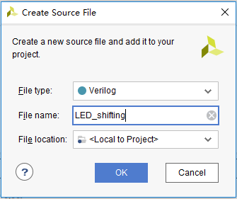
Figure 1.12 Create Source File dialog box
In the dialog box, set the file type and file name as follows.
- File type:Verilog
- File name:LED_shifting
- File location:Local to Project
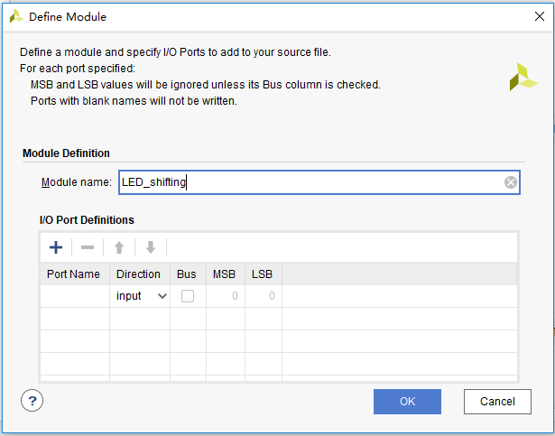
Figure 1.13 Define Module dialog box
The fifth step: click the OK button in Figure 1.12 to exit the Create Source File dialog.
The sixth step: add the LED_shifting.v file to the dialog shown in Figure 1.11.
The seventh step: click the Finish button in Figure 1.11 to bring up the Define Module dialog box, as shown in Figure 1.13.
In the Define Module dialog box, the port of the module can be defined, or in the later design file. This design directly defines the port in the Define Module dialog box. The input signal of the design are clock signal (differential clock) and external hardware reset signal, the output signal are 8 LEDs. Set the parameters according to the figure shown below. The setting result is shown in Figure 1.14.
- For clock signal, Port Name:inclk_p;Direction:input;
Port Name:inclk_n;Direction:input;
- For external reset signal, Port Name:rst;Direction:input;
- For 8-bit LED signal, Port Name: led; Direction: output; check the Bus option, set MSB to 7, and LSB to 0.
The eighth step: click the OK button to complete the creation of the design file. As shown in Figure 1.15, the LED_shifting.v file is added under the Design Sources folder in the Sources window.
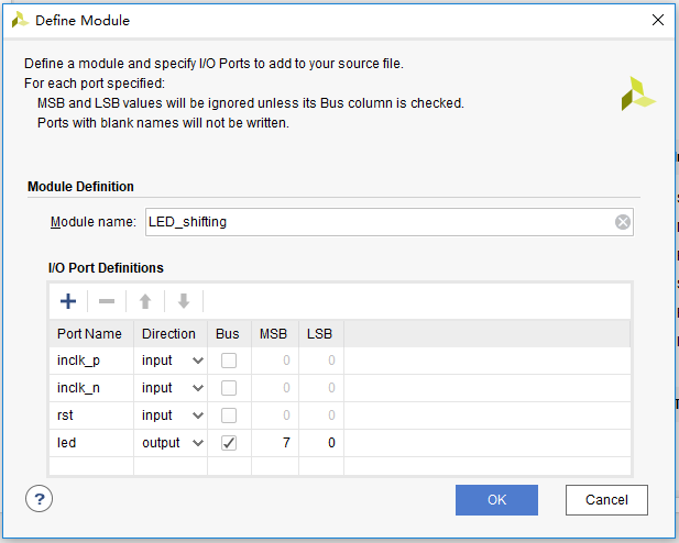
Figure 1.14 Define Module dialog box (for port difinition)
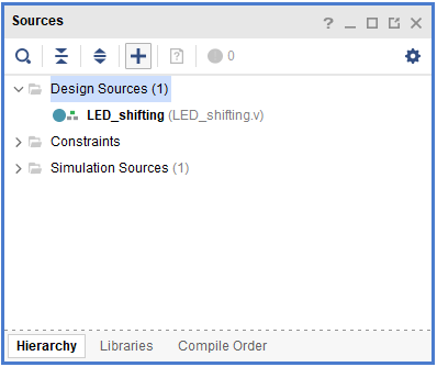
Figure 1.15 Add LED_shifting.v file
The ninth step: double-click the LED_shifting.v file to open the design file, as shown in Figure 1.16.
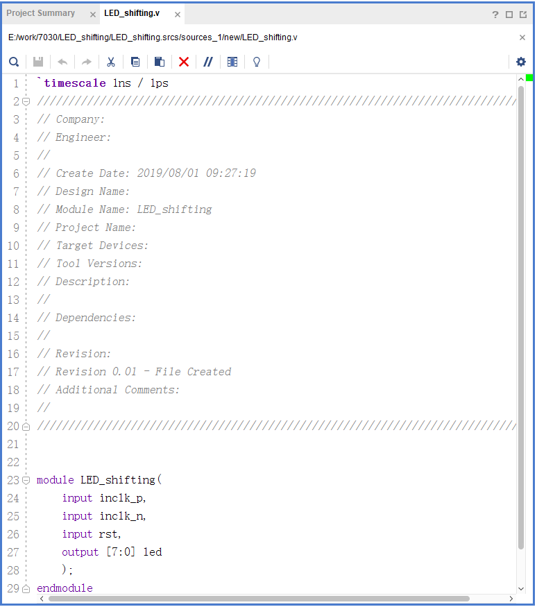
Figure 1.16 Design file interface
The tenth step: in the module of the design file, design and write the code. (If the module port is not defined in the Define Module dialog box, the design file is opened as shown in Figure 1.17 and needs to be defined here.)
Figure 1.17 Design file interface when the port is not defined in advance
1.3.3.3 Introduction to the Program
The first step: the establishment of the main program framework (port design)
| module LED_shifting(
input inclk_p, input inclk_n, input rst, output reg [7:0] led ); endmodule |
The input signals of this experiment have differential clock signals inclk_p and inclk_n, reset signal rst, and output signal 8-bit LED, which is defined by the bus form of led [7:0].
The second step: IP core invoking
In this experiment, a 100MHz clock is required as the operating clock of the following frequency division module, and the onboard input clock is a 200MHz differential clock, so the PLL frequency division is used to obtain a 100Mhz clock. Steps as follows.
- In the Flow Navigator on the left side of the Vivado main interface, select and expand the PORJECT MANAGER option to find the IP Catalog option, as shown in Figure 1.18.
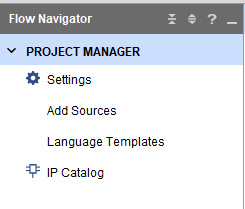
Figure 1.18 IP core
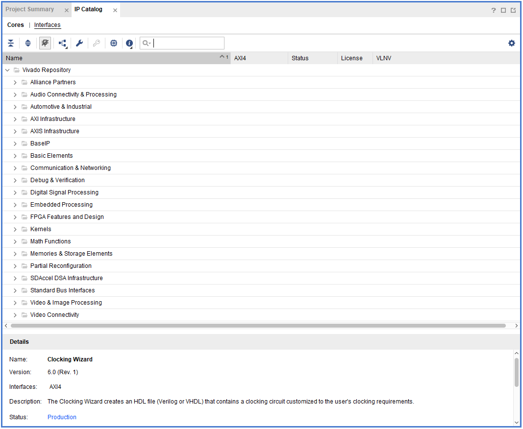
Figure 1.19 IP core content window
- Click IP Catalog, and the interface will pop up on the right side of the main interface. The IP addresses available in vIvado are in this directory, as shown in Figure 1.19.
- Use search to quickly find the IP core to use, enter clocking in the search bar, and the available clock IP core resources appear below, as shown in Figure 1.20, select the Clocking Wizard option.
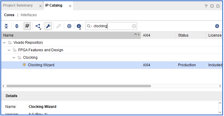
Figure 1.20 Searching for the target IP core
- Double-click the Clocking Wizard to bring up the Customize IP dialog box, as shown in Figure 1.21, set it according to the following parameters.
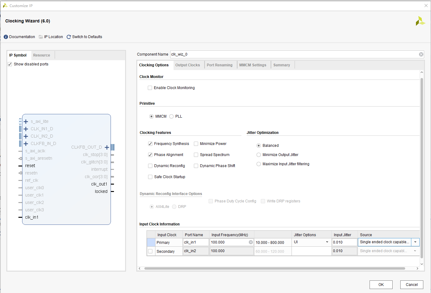
Figure 1.21 PLL setting interface
- In the Primitive interface, select the PLL, as shown in Figure 1.22.
- In the Clocking Options interface, the primary clock in the Input Clock Information dialog box, Input Frequency: 200; Source: Differential clock capable pin (the input clock is a differential clock with a frequency of 200MHz), as shown in Figure 1.23.
- In the Output Clocks interface, the output clock clk_out1, Output Freq: 100, Phase: 0, Duty Cycle: 50 (output clock is 100MHz, phase offset is 0, duty cycle is 50%) as shown in Figure 1.24.
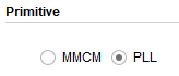
Figure 1.22 Choose PLL
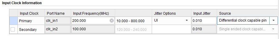
Figure 1.23 PLL Input Clock Settings
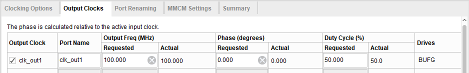
Figure 1.24 PLL output Clock Settings
- Click the OK button to complete the setup and the Generate Output Products dialog box will pop up. As shown in Figure 1.25.
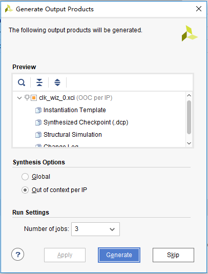
Figure 1.25 Generate Output Products dialog box
- Click the Generate button to generate the PLL.
In the Sources window of the main interface, click the IP Sources column, click the IP core PLL in the IP folder, expand the Instantiation Template, as shown in Figure 1.26, there is a PLL instantiation template file PLL.veo.
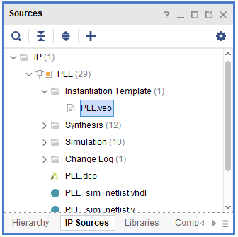
Figure 1.26 Generate an instantiation template for the PLL
The third step: instantiate the PLL into the design file
| wire sys_clk;
wire pll_locked; clk_wiz_0 clk_wiz_0_inst( .clk_in1_p (inclk_p), .clk_in1_n (inclk_n), .reset (1’b0), .locked (pll_locked), .clk_out1 (sys_clk) ); |
When the system is powered on, the locked signal has a value of 0 before the PLL locks (stable operation). locked is high after the PLL locks, and the clock signal sys_clk outputs normally.
The fourth step: determine the reset signal
sys_rst is used as the reset signal of the frequency division part, and ext_rst is used as the reset signal of the shifting LEDs. It is driven by the rising edge of the clock sys_clk, it is synchronously reset by the primary register.
| reg sys_rst;
reg ext_rst; always @ (posedge sys_clk) begin sys_rst <= !pll_locked; ext_rst <= rst; end |
The fifth step: design the frequency division
The design uses the 100MHz clock sysclk outputted by the PLL as the system clock. The experiment requires the moving speed of the shifting light to be 1 second. The frequency division design is used to first obtain the 1us after the microsecond frequency division, and then it is divided by milliseconds to get 1ms, and finally divided by seconds to get 1s clock.
- Microsecond frequency division
| reg [6:0] us_cnt;
reg us_f; always @ (posedge sys_clk) begin if (sys_rst) begin us_cnt <= 0; us_f <= 1’b0; end else begin us_f <= 1’b0; if (us_cnt == 99) begin us_cnt <= 0; us_f <= 1’b1; end else us_cnt <= us_cnt + 1’b1; end end |
The 100MHz clock has a period of 10ns, and 1us requires 100 clock cycles, that is, 100 10ns. Therefore, a microsecond counter us_cnt [6:0] and a microsecond pulse signal us_f are defined. The counter is cleared at reset. On each rising edge of the clock, the counter is incremented by one. When the counter is equal to 99, the period of 1us elapses, and the microsecond pulse signal us_f is pulled high. Thus, every 1us, this module will generate a pulse signal.
- Millisecond frequency division
Similarly, 1ms is equal to 1000 1us, a millisecond counter ms_cnt [9:0], a microsecond pulse signal ms_f are defined.
| reg [9:0] ms_cnt;
reg ms_f; always @ (posedge sys_clk) begin if (sys_rst) begin ms_cnt <= 0; ms_f <= 1’b0; end else begin ms_f <= 1’b0; if (us_f) begin if (ms_cnt == 999) begin ms_cnt <= 0; ms_f <= 1’b1; end else ms_cnt <= ms_cnt + 1’b1; end end end |
- Second frequency division
Define a second counter s_cnt [9:0], one second pulse signal s_f. When the three counters are simultaneously full, the time passes for 1 s and the second pulse signal is issued.
| reg [9:0] s_cnt;
reg s_f; always @ (posedge sys_clk) begin if (sys_rst) begin s_cnt <= 0; s_f <= 1’b0; end else begin s_f <= 1’b0; if (ms_f) begin if (s_cnt == 999) begin s_cnt <=0; s_f <= 1’b1; end else s_cnt <= s_cnt + 1’b1; end end end |
The sixth step: shifting LED design
When resetting, 8 LED lights are all on, so the value of the output led is 8’hff. Then the LED light needs to shift, so at first the lowest LED is lit. At this time, the value of led is 8’b0000_0001, when the second pulse signal arrives, the next LED light is turned on. At this time, the value of led is 8’b0000_0010. It can be seen that as long as the high level of “1” is shifted to the left, it can be realized by bit splicing, that is, led <= {led[6:0], led[7]}.
| always @ (posedge sys_clk)
begin if (ext_rst) led <= 8’hff; else begin if (led == 8’hff) led <= 8’b0000_0001; else if (s_f) led <= {led[6:0], led[7]}; end end |
1.4 Experiment Verification
The first step: design synthesis
- Expand the SYNTHESIS option under the Flow Nvigator window on the left side of the Vivado main interface, and click Run Synthesis to perform the design synthesis. There are two purposes.
- Check for syntax errors
- Forming a tree-like hierarchical relationship of the project
- After the integration is complete, the Synthesis Completed dialog box is displayed, as shown in Figure 1.27. Select Open Synthesized Design and click the OK button to open the analysis and the integrated design.
The second step: add the constraint
After the integration process is successfully completed, a consolidated netlist is generated. Before implementing the board verification, the pins and some other signals need to be constrained. There are two ways to implement constraints. One is to use the I/O planning function in Vivado, and the other is to directly create an XDC constraint file and manually enter the constraint command. The first method was used in this experiment.
- After completing the previous step, in the opening integrated design, click Layout on the Vivado menu bar, the floating command window appears, and select the I/O planning command, as shown in Figure 1.28.
- After executing the command, the Vivado main interface automatically jumps to the I/O pin assignment interface, as shown in Figure 1.29. The upper Package window shows the device package and I/O distribution, and the lower I/O Ports window shows all the I/O port information of the design.
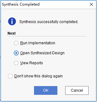
Figure 1.27 Synthesis Completed dialog box
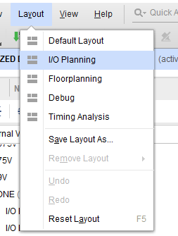
Figue 1.28 Excute I/O planning
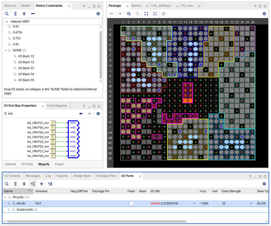
Figure 1.29 Pin assignment interface
- Pin assignment for each I / O, the pin mapping table is shown in Table 1.1, and the allocation result is shown in Figure 1.30.
Table 1.1 LED shifting experiment pin mapping table
| Signal Name | Network Name | FPGA Pin | Port Description |
| inclk_p | SYSCLK_P | AC13 | Input clock(differential)
200MHz |
| inclk_n | SYSCLK_N | AD13 | |
| rst | GPIO_SW_2 | F4 | External reset |
| led[0] | GPIO_DIP_SW0 | A17 | 8-bit LED |
| led[1] | GPIO_DIP_SW1 | E8 | |
| led[2] | GPIO_DIP_SW2 | C6 | |
| led[3] | GPIO_DIP_SW3 | B9 | |
| led[4] | GPIO_DIP_SW4 | B6 | |
| led[5] | GPIO_DIP_SW5 | H6 | |
| led[6] | GPIO_DIP_SW6 | H7 | |
| led[7] | GPIO_DIP_SW7 | G9 |
Figure 1.30 Pin assignment
The third step: implementation
After the pin assignment is completed, expand IMPLEMENTATION in the Flow Navigator window on the left side of the Vivado main interface, click Run Implementation, and the Save Constraints dialog box pops up, as shown in Figure 1.31.
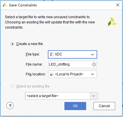
Figure 1.31 Save Constraints dialog box
The fourth step: generate programmable files
After completing the previous step, expand PROGRAM AND DEBUG in the Flow Navigator window on the left side of the main interface of Vivado. Click Generate Bitstream to generate a programmable bitstream file.
The fifth step: board verification
With the Zynq_7030 development board connected, expand the Open Hardware Manager, click Open Target, a floating command window appears, and choose to execute the Auto Connect command, as shown in Figure 1.32. Vivado will automatically search for the device, as shown in Figure 1.33. Successfully connected development board.
As shown in Figure 1.34, click Program device in the figure, the Program Device dialog box pops up, as shown in Figure 1.35. Select the correct bit stream (.bit) file, and click Program to download the file to FII-PRA100T development board.
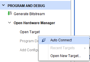
Figure 1.32 Execute Auto Connect command
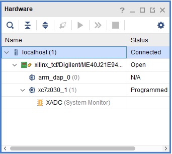
Figure 1.33 Successfully connected development board
![]()
Figure 1.34 Open program device
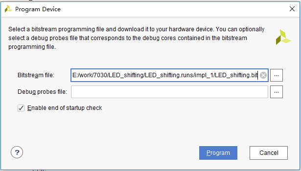
Figure 1.35 Program Device dialog box
The experimental phenomenon is shown in Figure 1.36.
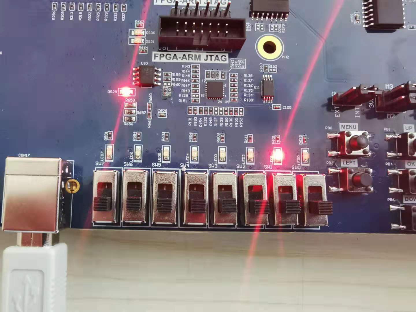
Figure 1.36 Experimental phenomenon of LED shifting