Zynq_7030 Development System FII-PE7030
System Design Objective
The main purpose of this system design is to complete FPGA learning, development and experiment with Xilin-Vivado. The main device uses the XC7Z030-1FFG676C. The main learning and development projects can be completed as follows:
(1)Basic FPGA design training
(2)Construction and training of the SOPC (Microblaze) system
(3)IC design and verification, the system provides hardware design, simulation and verification of RISC-V CPU.
(4)Based on RISC-V development and application.
(5)The system is specifically optimized for hardware design for RISC-V system applications.
2、System Resource
- Extended memory: two DDR3 (PL end) four DDR3 (PS end)
- 32M serial FLASH memory
- Serial EEPROM
- Gigabit Ethernet (one for PS end and one for PL end)
- USB to serial interface: USB-UART bridge
3、Human-computer Interaction Interface
- 8-bit DIP switches
- A total of 8 push buttons, 7 of which are defined as (MENU, UP, RETUN, LEFT, OK, RIGHT, DOWN), one push button is defined as FPGA hardware reset (RESET)
- 8-bit LED
- 6 7-segment display
- I2C bus interface
- Two JTAG programming interfaces: one for the FPGA download debug interface, one for the RISC-V CPU JTAG debug interface
- Built-in RISC-V CPU software debugger, no external RISC-V JTAG emulator required
- One 12-pin GPIO connector, in line with PMOD interface standard
4、Software Development System
- Vivado 18.1 and later version for FPGA development, Microblaze SOPC
- Freedom Studio-Win_x86_64 Software development for RISC-V CPU
5. Supporting Resources
RISC-V JTAG Debugger
Xilinx JTAG Download Debugger
FII-PE7030 PE7030 Harware Reference Guide
FII-PE7030 PE7030 User Experimental Manual
6、Physical Display
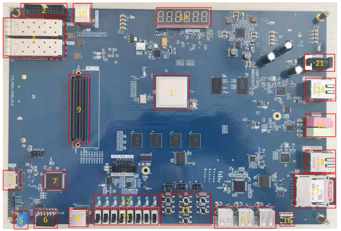
Figure 1 FII-PE7030 physical picture
Corresponding to the physical picture, the main components of the development board are as follows:
1:ZYNQ_7030 chip
2:RISCV_JTAG download port
3:Fiber interface
4:HDMI interface
5:Potentiometer
6:GPIO interface
7:HDMI chip (ADV7511)
8:FPGA download port
9:FMC interface
10:RISC-V download port
11:8-bit DIP switch
12:8-bit LED
13:7 push buttons
14:6 seven-segment display
15:USB interface
16:reset button (RESET)
17:SD card
18:Ethernet interface (PS end)
19:Audio output (green) and audio input (red)
20:Ethernet interface (PL end)
21:External 12V power connector