
Description
FII-BD9361 – Perfectly compatible with AD-FMCOMMS3-EBZ – Code compatible, development tool compatible, performance compatible, Smaller size and more space saving
– AD9361 Software Development Kit using the AD9361 RF Agile Transceiver
The FII-BD9361 is a high-speed analog module designed to showcase the AD9361, a high performance, highly integrated RF transceiver intended for use in RF applications, such as 3G and 4G base station and test equipment applications, and software defined radios. Its program-ability and wide-band capability make it ideal for a broad range of transceiver applications. The device combines an RF front end with a flexible mixed-signal base-band section and integrated frequency synthesizers, simplifying design-in by providing a configurable digital interface to a processor or FPGA. ( FII-BD9371 is used for 3G to 5G base station )
The AD9361 chip operates in the 70 MHz to 6 GHz range, covering most licensed and unlicensed bands. The chip supports channel bandwidths from less than 200 kHz to 56 MHz by changing sample rate, digital filters, and decimation, which re all programmable within the AD9361 itself.
FII-BD9361 Features and Benefits
-
Software tunable across wide frequency range : TX :47 MHz to 6 GHz RX:70 MHz to 6 GHz
-
Software tunable bandwidth: 200 kHz to 56 MHz.
-
Software tunable TX Power and RX Dynamic Range:TX>80dB RX>70dB
-
Powered up from single standard FMC connector
-
Supports MIMO radio,2 ways TX and 2 ways RX(Max 4T4R by RF Switches configuration)
-
Supports FII-7030 and other standard FMC Connector Platform software radio application
-
TX Power higher, Broadband flatness is better.
FII-BD9361 Product Details – Completely Compatible with AD-FMCOMMS3-EBZ Board
-
The FII-BD9361 is a high-speed analog module designed to showcase the AD9361, a high performance, highly integrated RF transceiver intended for use in RF applications, such as 3G and 4G base station and test equipment applications, and software defined radios. Its programmability and wideband capability make it ideal for a broad range of transceiver applications.
-
The device combines an RF front end with a flexible mixed-signal baseband section and integrated frequency synthesizers, simplifying design-in by providing a configurable digital interface to a processor or FPGA. The AD9361 chip operates in the 70 MHz to 6 GHz range, covering most licensed and unlicensed bands. The chip supports channel bandwidths from less than 200 kHz to 56 MHz by changing sample rate, digital filters, and decimation, which are all programmable.
Block Diagram and Interface
System Block Diagram
| Interface Type | Definition | Description |
| SMA-F | TX1A, TX2A | 2 x RF transmission channel (same frequency) |
| SMA-F | RX1A, RX2A | 2 x RF receiving channel (same frequency) |
| UMC-F | TX1B, TX2B | 2 x RF transmission channel (reference to channel A) |
| UMC-F | RX1B, RX2B | 2 x RF transmission channel (reference to channel B) |
| UMC-F | TXLO | External transmission reference oscillator |
| UMC-F | RXLO | External receiving reference oscillator |
| UMC-F | REF | External reference clock |
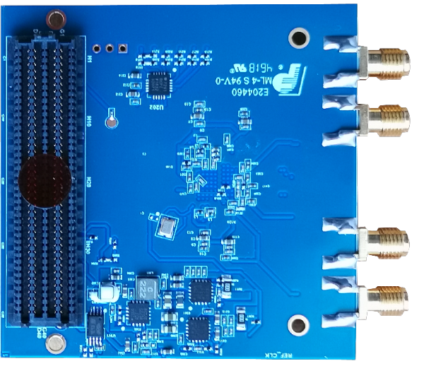
| LPC FMC | FMC | Refer the schematics for universal RF transmission interface, compatible with similar products in most markets |
Peripheral interface table
FMC-LPC Definition
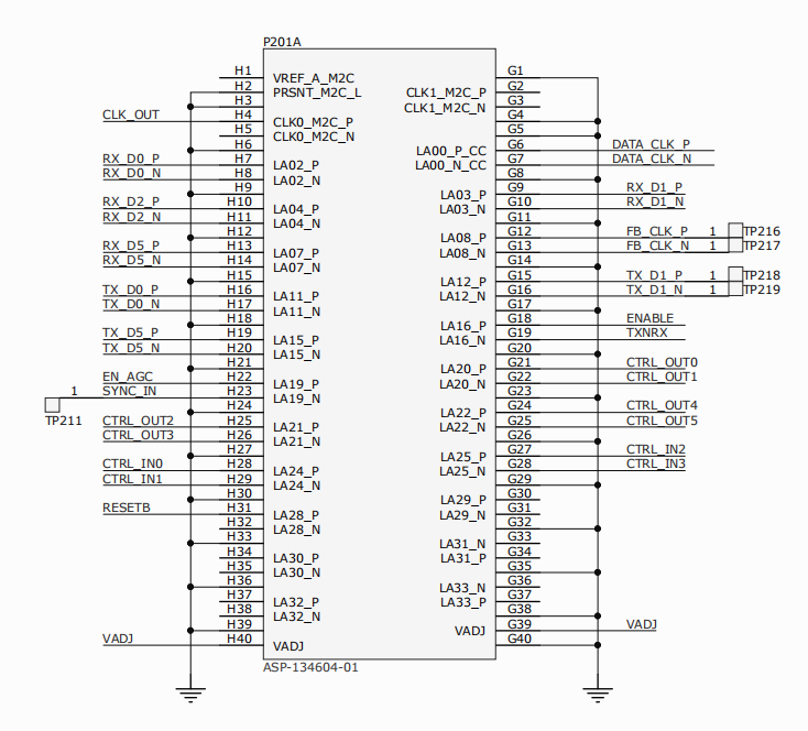
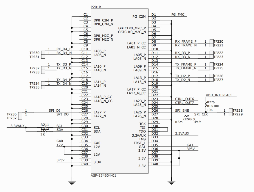
FMC-LPC Definition(compatible with AD-FMCOMMS3)
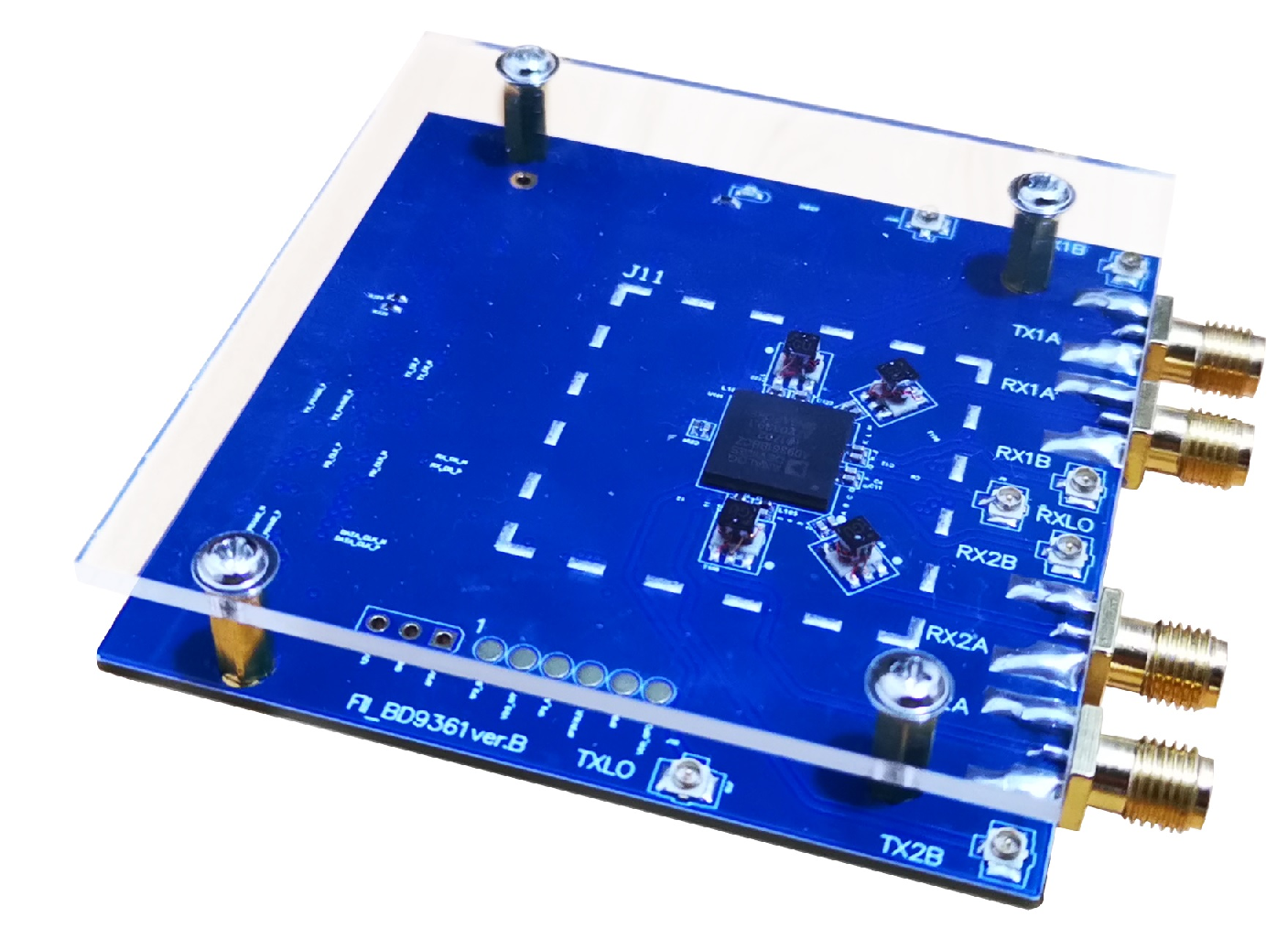
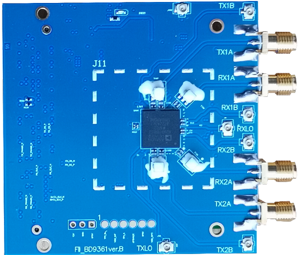
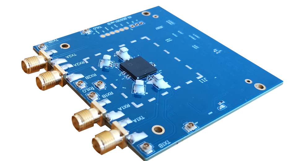
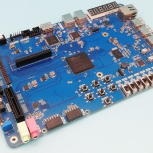
FII-BD9361 Interface:
Digital Interface:FMC-LPC
RF Interface: Four Way Differential Transceiver
FII-BD9361 Features
We support all features of AD-FMCOMMS3-EBZ such as:
TX band: 47 MHz to 6.0 GHz
RX band: 70 MHz to 6.0 GHz
Bandwidth Adjustment Range: 200 kHz to 56 MHz
Low noise figure: 2dB NF(noise figure/800MHz )
LO ,RX Gain Control,AGC
2.4Hhz local oscillator (LO) step
For more information, please check ad9361 introduction.
FII-BD9361 Applications
-
-
- General purpose design for any software-designed radio application
- MIMO radio
- Point to point communication systems
- Femtocell/picocell/microcell base stations
- USRP
- 3G/4G signal and protocol analysis
- WiFi
- ISM
-
3. Compatible Boards
AD-FMCOMMS3-EBZ (FII-BD9361 the same as )
(https://www.analog.com/en/design-center/evaluation-hardware-and-software/evaluation-boards-kits/eval-ad-fmcomms3-ebz.html#eb-overview)
4. Support Boards
ZC702
ZC706
Zedboard
FII-PE7030
5. User Guide : (FII-BD9361 can use it )
https://wiki.analog.com/resources/eval/user-guides/ad-fmcomms3-ebz
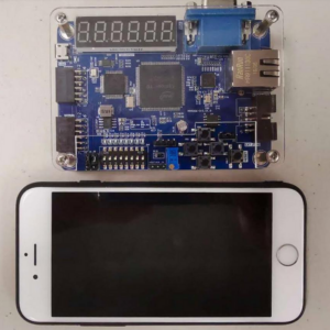
FII-BD9361 Hardware Configuration
FII-BD9361 is developed by Fraser Innovation INC. It is absolutely compatible with AD-FMComms3-EBZ Board. The purpose of the AD-FMComms3-EBZ is to provide an RF platform to software developers, system architects, etc, who want a single platform which operates over a much wider tuning range (70 MHz – 6 GHz). It’s expected that the RF performance of this platform can meet the datasheet specifications at 2.4 GHz, but not at the entire RF tuning range that the board supports (but it will work much better than the AD-FMCOMMS2-EBZ over the complete RF frequency). We will provide typical performance data for the entire range (70 MHz – 6 GHz) which is supported by the platform.
This is primarily for system investigation and bring up of various waveforms from a software team before their custom hardware is complete, where they want to see waveforms, but are not concerned about the last 1dB or 1% EVM of performance.
You can find the user guide in above link at analog website. We will send you hardware configuration and system Scheme Diagram when you purchase this products.
4. System Scheme Diagram
![]()
5. Peripheral Interfaces

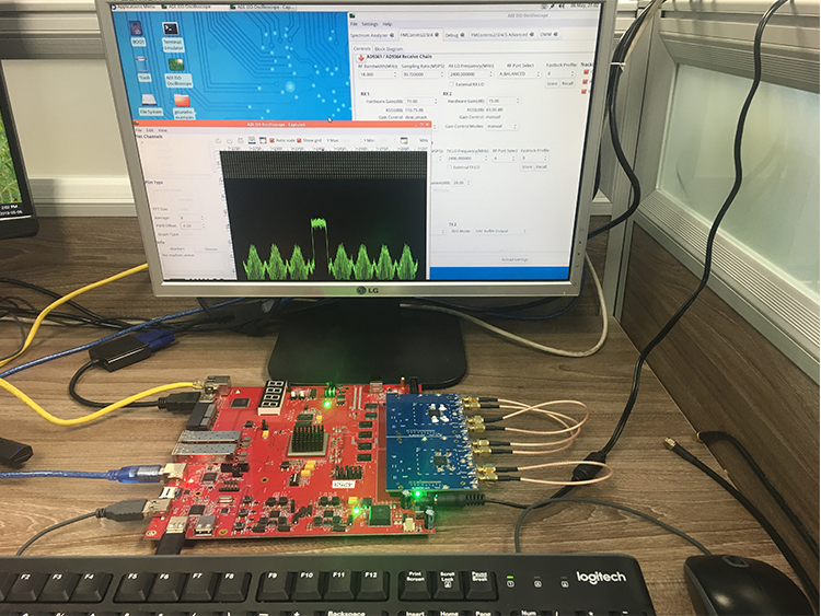
6. testing scenarios

FII-AD9361 – Test data reference (part of the project)
1. Output power and flatness test
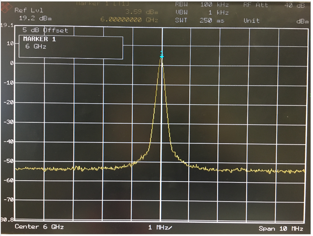
Test summary: The above picture shows some test screenshots, the frequency range covers from 70MHz to 6GHz, 150MHz to 6GHz output power 3-8dBm, high performance RF balun design guarantees high bandwidth and high flatness.
2. Phase noise test
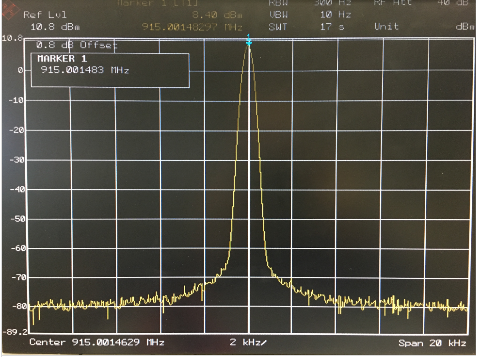
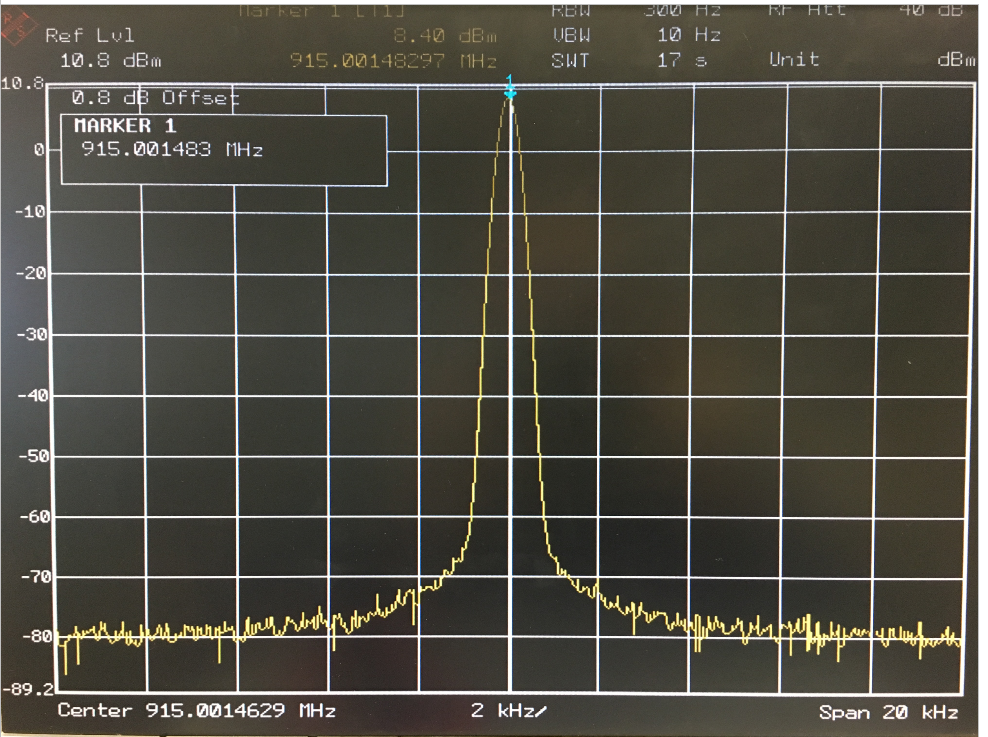
Test summary: The above picture is a partial test screenshot, the frequency range covers from 70MHz to 6GHz, 6GHz phase noise typical value is 90dBc/1KHz, 100dBc/10KHz, perfect phase noise guarantees high quality communication test requirements.
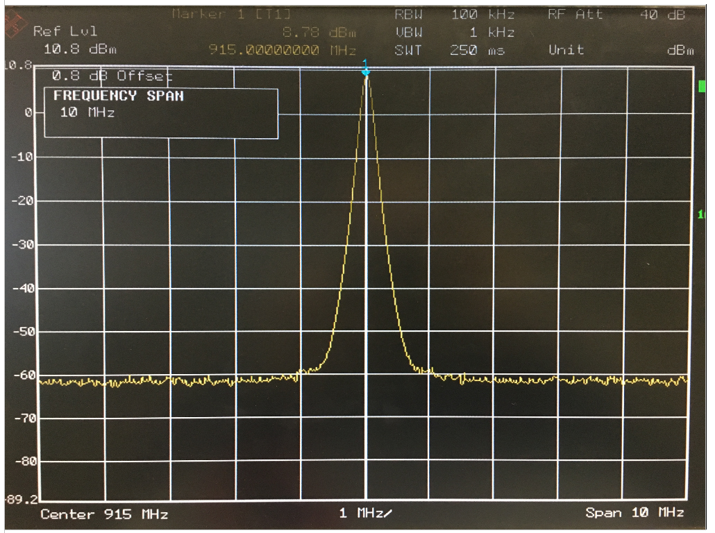
3. IQ modulation function test
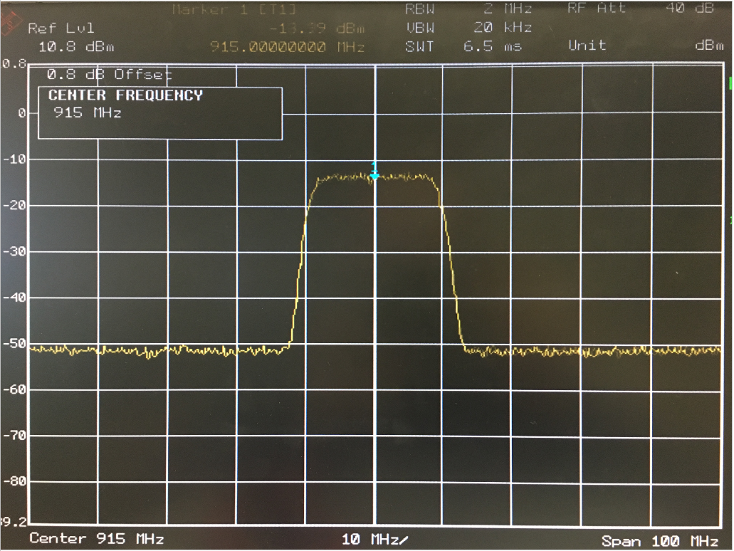
Test summary: The above figure shows the spectrum signal output of QPSK modulated at 915M frequency 20M, and the IQ modulation function is normal.
AD9361 RF Agile Transceiver
Learn about the revolutionary AD9361 RF Agile Transceiver, a complete radio design for SDR applications. It achieves leading performance, high integration, wideband operation and utmost flexibility and is supported by the FII-BD9361 board.
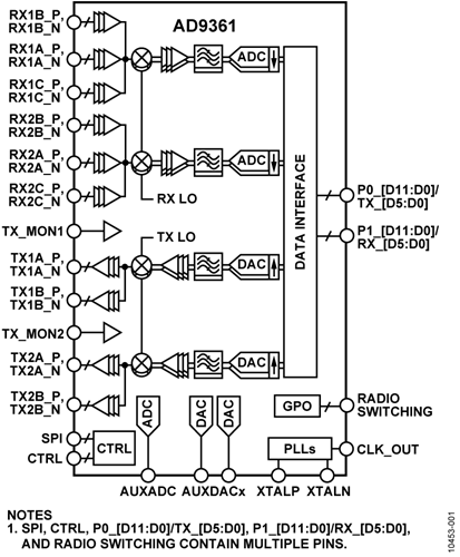
AD9361 Product Details
The AD9361 is a high performance, highly integrated radio frequency (RF) Agile Transceiver™ designed for use in 3G and 4G base station applications. Its programmability and wideband capability make it ideal for a broad range of transceiver applications. The device combines a RF front end with a flexible mixed-signal baseband section and integrated frequency synthesizers, simplifying design-in by providing a configurable digital interface to a processor. The AD9361 receiver LO operates from 70 MHz to 6.0 GHz and the transmitter LO operates from 47 MHz to 6.0 GHz range, covering most licensed and unlicensed bands. Channel bandwidths from less than 200 kHz to 56 MHz are supported.
The two independent direct conversion receivers have state-of-the-art noise figure and linearity. Each receive (RX) subsystem includes independent automatic gain control (AGC), dc offset correction, quadrature correction, and digital filtering, thereby eliminating the need for these functions in the digital baseband. The AD9361 also has flexible manual gain modes that can be externally controlled. Two high dynamic range analog-to-digital converters (ADCs) per channel digitize the received I and Q signals and pass them through configurable decimation filters and 128-tap finite impulse response (FIR) filters to produce a 12-bit output signal at the appropriate sample rate.
The transmitters use a direct conversion architecture that achieves high modulation accuracy with ultralow noise. This transmitter design produces a best in class TX error vector magnitude (EVM) of <−40 dB, allowing significant system margin for the external power amplifier (PA) selection. The on-board transmit (TX) power monitor can be used as a power detector, enabling highly accurate TX power measurements.
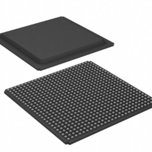
The fully integrated phase-locked loops (PLLs) provide low power fractional-N frequency synthesis for all receive and transmit channels. Channel isolation, demanded by frequency division duplex (FDD) systems, is integrated into the design. All VCO and loop filter components are integrated. The core of the AD9361 can be powered directly from a 1.3 V regulator. The IC is controlled via a standard 4-wire serial port and four real-time input/output control pins. Comprehensive power-down modes are included to minimize power consumption during normal use. The AD9361 is packaged in a 10 mm × 10 mm, 144-ball chip scale package ball grid array (CSP_BGA).
AD9361 Product Features:
RF 2 × 2 transceiver with integrated 12-bit DACs and ADCs
TX band: 47 MHz to 6.0 GHz
RX band: 70 MHz to 6.0 GHz
Supports TDD and FDD operation
Tunable channel bandwidth: <200 kHz to 56 MHz
Dual receivers: 6 differential or 12 single-ended inputs
Superior receiver sensitivity with a noise figure of 2 dB at 800 MHz LO
RX gain control
Real-time monitor and control signals for manual gain
Independent automatic gain control
Dual transmitters: 4 differential outputs
Highly linear broadband transmitter
TX EVM: ≤−40 dB
TX noise: ≤−157 dBm/Hz noise floor
TX monitor: ≥66 dB dynamic range with 1 dB accuracy
Integrated fractional-N synthesizers
2.4 Hz maximum local oscillator (LO) step size
Multichip synchronization
CMOS/LVDS digital interface

AD9361 Applications
- Point to point communication systems
- Femtocell/picocell/microcell base stations
- General-purpose radio systems
Click following link for AD9361 Datasheet
AD9361 Theory of Operation
GENERAL
The AD9361 is a highly integrated radio frequency (RF) transceiver capable of being configured for a wide range of applications. The device integrates all RF, mixed signal, and digital blocks necessary to provide all transceiver functions in a single device. Programmability allows this broadband transceiver to be adapted for use with multiple communication standards, including frequency division duplex (FDD) and time division duplex (TDD) systems. This programmability also allows the device to be interfaced to various baseband processors (BBPs) using a single 12-bit parallel data port, dual 12-bit parallel data ports, or a 12-bit low voltage differential signaling (LVDS) interface.
The AD9361 also provides self-calibration and automatic gain control (AGC) systems to maintain a high performance level under varying temperatures and input signal conditions. In addition, the device includes several test modes that allow system designers to insert test tones and create internal loopback modes that can be used by designers to debug their designs during prototyping and optimize their radio configuration for a specific application.
RECEIVER
The receiver section contains all blocks necessary to receive RF signals and convert them to digital data that is usable by a BBP. There are two independently controlled channels that can receive signals from different sources, allowing the device to be used in multiple input, multiple output (MIMO) systems while sharing a common frequency synthesizer.
Each channel has three inputs that can be multiplexed to the signal chain, making the AD9361 suitable for use in diversity systems with multiple antenna inputs. The receiver is a direct conversion system that contains a low noise amplifier (LNA), followed by matched in-phase (I) and quadrature (Q) amplifiers, mixers, and band shaping filters that down convert received signals to baseband for digitization. External LNAs can also be interfaced to the device, allowing designers the flexibility to customize the receiver front end for their specific application.
Gain control is achieved by following a preprogrammed gain index map that distributes gain among the blocks for optimal performance at each level. This can be achieved by enabling the internal AGC in either fast or slow mode or by using manual gain control, allowing the BBP to make the gain adjustments as needed. Additionally, each channel contains independent RSSI measurement capability, dc offset tracking, and all circuitry necessary for self-calibration.
The receivers include 12-bit, Σ-Δ ADCs and adjustable sample rates that produce data streams from the received signals. The digitized signals can be conditioned further by a series of decimation filters and a fully rogrammable 128-tap FIR filter with additional decimation settings. The sample rate of each digital filter block is adjustable by changing decimation factors to produce the desired output data rate.
TRANSMITTER
The transmitter section consists of two identical and independently controlled channels that provide all digital processing, mixed signal, and RF blocks necessary to implement a direct conversion system while sharing a common frequency synthesizer. The digital data received from the BBP passes through a fully programmable 128-tap FIR filter with interpolation options. The FIR output is sent to a series of interpolation filters that provide additional filtering and data rate interpolation prior to reaching the DAC.
Each 12-bit DAC has an adjustable sampling rate. Both the I and Q channels are fed to the RF block for upconversion. When converted to baseband analog signals, the I and Q signals are filtered to remove sampling artifacts and fed to the upconversion mixers. At this point, the I and Q signals are recombined and modulated on the carrier frequency for transmission to the output stage. The combined signal also passes through analog filters that provide additional band shaping, and then the signal is transmitted to the output amplifier. Each transmit channel provides a wide attenuation adjustment range with fine granularity to help designers optimize signal-to-noise ratio (SNR).
Self-calibration circuitry is built into each transmit channel to provide automatic real-time adjustment. The transmitter block also provides a TX monitor block for each channel. This block monitors the transmitter output and routes it back through an unused receiver channel to the BBP for signal monitoring. The TX monitor blocks are available only in TDD mode operation while the receiver is idle.
CLOCK INPUT OPTIONS
The AD9361 operates using a reference clock that can be provided by two different sources. The first option is to use a dedicated crystal with a frequency between 19 MHz and 50 MHz connected between the XTALP and XTALN pins. The second option is to connect an external oscillator or clock distribution device (such as the AD9548) to the XTALN pin (with the XTALP pin remaining unconnected). If an external oscillator is used, the frequency
can vary between 10 MHz and 80 MHz. This reference clock is used to supply the synthesizer blocks that generate all data clocks, sample clocks, and local oscillators inside the device.
Errors in the crystal frequency can be removed by using the digitally programmable digitally controlled crystal oscillator (DCXO) function to adjust the on-chip variable capacitor. This capacitor can tune the crystal frequency variance out of the system, resulting in a more accurate reference clock from which all other frequency signals are generated. This function can also be used with on-chip temperature sensing to provide oscillator frequency temperature compensation during normal operation.
SYNTHESIZERS
RF PLLs
The AD9361 contains two identical synthesizers to generate the required LO signals for the RF signal paths:—one for the receiver and one for the transmitter. Phase-locked loop (PLL) synthesizers are fractional-N designs incorporating completely integrated voltage controlled oscillators (VCOs) and loop filters. In TDD operation, the synthesizers turn on and off as appropriate for the RX and TX frames. In FDD mode, the TX PLL and the RX PLL
can be activated simultaneously. These PLLs require no external components.
BB PLL
The AD9361 also contains a baseband PLL synthesizer that is used to generate all baseband related clock signals. These include the ADC and DAC sampling clocks, the DATA_CLK signal (see the Digital Data Interface section), and all data framing signals. This PLL is programmed from 700 MHz to 1400 MHz based on the data rate and sample rate requirements of the system.
DIGITAL DATA INTERFACE
The AD9361 data interface uses parallel data ports (P0 and P1) to transfer data between the device and the BBP. The data ports can be configured in either single-ended CMOS format or differential LVDS format. Both formats can be configured in multiple arrangements to match system requirements for data ordering and data port connections. These arrangements include single port data bus, dual port data bus, single data rate, double data rate,
and various combinations of data ordering to transmit data from different channels across the bus at appropriate times.
Bus transfers are controlled using simple hardware handshake signaling. The two ports can be operated in either bidirectional (TDD) mode or in full duplex (FDD) mode where half the bits are used for transmitting data and half are used for receiving data. The interface can also be configured to use only one of the data ports for applications that do not require high data rates and prefer to use fewer interface pins.
DATA_CLK Signal
RX data supplies the DATA_CLK signal that the BBP can use when receiving the data. The DATA_CLK can be set to a rate that provides single data rate (SDR) timing where data is sampled on each rising clock edge, or it can be set to provide double data rate (DDR) timing where data is captured on both rising and falling edges. This timing applies to operation using either a single port or both ports.
FB_CLK Signal
For transmit data, the interface uses the FB_CLK signal as the timing reference. FB_CLK allows source synchronous timing with rising edge capture for burst control signals and either rising edge (SDR mode) or both edge capture (DDR mode) for transmit signal bursts. The FB_CLK signal must have the same frequency and duty cycle as DATA_CLK.
RX_FRAME Signal
The device generates an RX_FRAME output signal whenever the receiver outputs valid data. This signal has two modes: level mode (RX_FRAME stays high as long as the data is valid) and pulse mode (RX_FRAME pulses with a 50% duty cycle). Similarly, the BBP must provide a TX_FRAME signal that indicates the beginning of a valid data transmission with a rising edge. Similar to the RX_FRAME, the TX_FRAME signal can remain high
throughout the burst or it can be pulsed with a 50% duty cycle.
ENABLE STATE MACHINE
The AD9361 transceiver includes an enable state machine (ENSM) that allows real-time control over the current state of the device.
The device can be placed in several different states during normal operation, including
• Wait—power save, synthesizers disabled
• Sleep—wait with all clocks/BB PLL disabled
• TX—TX signal chain enabled
• RX—RX signal chain enabled
• FDD—TX and RX signal chains enabled
• Alert—synthesizers enabled
The ENSM has two possible control methods: SPI control and pin control.
SPI Control Mode
In SPI control mode, the ENSM is controlled asynchronously by writing SPI registers to advance the current state to the next state. SPI control is considered asynchronous to the DATA_CLK because the SPI_CLK can be derived from a different clock reference and can still function properly. The SPI control ENSM method is recommended when real-time control of the synthesizers is not necessary. SPI control can be used for realtime control as long as the BBIC has the ability to perform timed SPI writes accurately.
Pin Control Mode
In pin control mode, the enable function of the ENABLE pin and the TXNRX pin allow real-time control of the current state.
The ENSM allows TDD or FDD operation depending on the configuration of the corresponding SPI register. The ENABLE and TXNRX pin control method is recommended if the BBIC has extra control outputs that can be controlled in real time, allowing a simple 2-wire interface to control the state of the device. To advance the current state of the ENSM to the next state, the enable function of the ENABLE pin can be driven by either a pulse (edge detected internally) or a level.
When a pulse is used, it must have a minimum pulse width of one FB_CLK cycle. In level mode, the ENABLE and TXNRX pins are also edge detected by the AD9361 and must meet the same minimum pulse width requirement of one FB_CLK cycle.
In FDD mode, the ENABLE and TXNRX pins can be remapped to serve as real-time RX and TX data transfer control signals. In this mode, the ENABLE pin enables or disables the receive signal path, and the TXNRX pin enables or disables the transmit signal path. In this mode, the ENSM is removed from the system for control of all data flow by these pins.
SPI INTERFACE
The AD9361 uses a serial peripheral interface (SPI) to communicate with the BBP. This interface can be configured as a 4-wire interface with dedicated receive and transmit ports, or it can be configured as a 3-wire interface with a bidirectional data communication port. This bus allows the BBP to set all device control parameters using a simple address data serial bus protocol.
Write commands follow a 24-bit format. The first six bits are used to set the bus direction and number of bytes to transfer. The next 10 bits set the address where data is to be written. The final eight bits are the data to be transferred to the specified register address (MSB to LSB). The AD9361 also supports an LSB-first format that allows the commands to be written in LSB to MSB format. In this mode, the register addresses are incremented for
multibyte writes.
Read commands follow a similar format with the exception that the first 16 bits are transferred on the SPI_DI pin and the final eight bits are read from the AD9361, either on the SPI_DO pin in 4-wire mode or on the SPI_DI pin in 3-wire mode.
CONTROL PINS
Control Outputs (CTRL_OUT[7:0])
The AD9361 provides eight simultaneous real-time output signals for use as interrupts to the BBP. These outputs can be configured to output a number of internal settings and measurements that the BBP can use when monitoring transceiver performance in different situations. The control output pointer register selects what information is output to these pins, and the control output enable register determines which signals are activated for monitoring by the BBP.
Signals used for manual gain mode, calibration flags, state machine states, and the ADC output are among the outputs that can be monitored on these pins.
Control Inputs (CTRL_IN[3:0])
The AD9361 provides four edge detected control input pins. In manual gain mode, the BBP can use these pins to change the gain table index in real time. In transmit mode, the BBP can use two of the pins to change the transmit gain in real time.
GPO PINS (GPO_3 TO GPO_0)
The AD9361 provides four, 3.3 V capable general-purpose logic output pins: GPO_3, GPO_2, GPO_1, and GPO_0. These pins can be used to control other peripheral devices such as regulators and switches via the AD9361 SPI bus, or they can function as slaves for the internal AD9361 state machine.
AUXILIARY CONVERTERS
AUXADC
The AD9361 contains an auxiliary ADC that can be used to monitor system functions such as temperature or power output. The converter is 12 bits wide and has an input range of 0 V to 1.25 V. When enabled, the ADC is free running. SPI reads provide the last value latched at the ADC output. A multiplexer in front of the ADC allows the user to select between the AUXADC input pin and a built-in temperature sensor.
AUXDAC1 and AUXDAC2
The AD9361 contains two identical auxiliary DACs that can provide power amplifier (PA) bias or other system functionality. The auxiliary DACs are 10 bits wide, have an output voltage range of 0.5 V to VDD_GPO − 0.3 V, a current drive of 10 mA, and can be directly controlled by the internal enable state machine.
POWERING THE AD9361
The AD9361 must be powered by the following three supplies:
the analog supply (VDDD1P3_DIG/VDDAx = 1.3 V), the interface supply (VDD_INTERFACE = 1.8 V), and the GPO supply (VDD_GPO = 3.3 V).
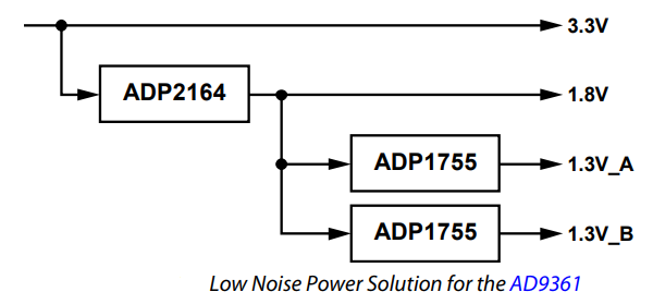
For applications requiring optimal noise performance, it is recommended that the 1.3 V analog supply be split and sourced from low noise, low dropout (LDO) regulators. Following figure shows the recommended method.
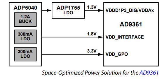
For applications where board space is at a premium, and optimal noise performance is not an absolute requirement, the 1.3 V analog rail can be provided directly from a switcher, and a more integrated power management unit (PMU) approach can be adopted. Following figure shows this approach.
Reviews
There are no reviews yet.