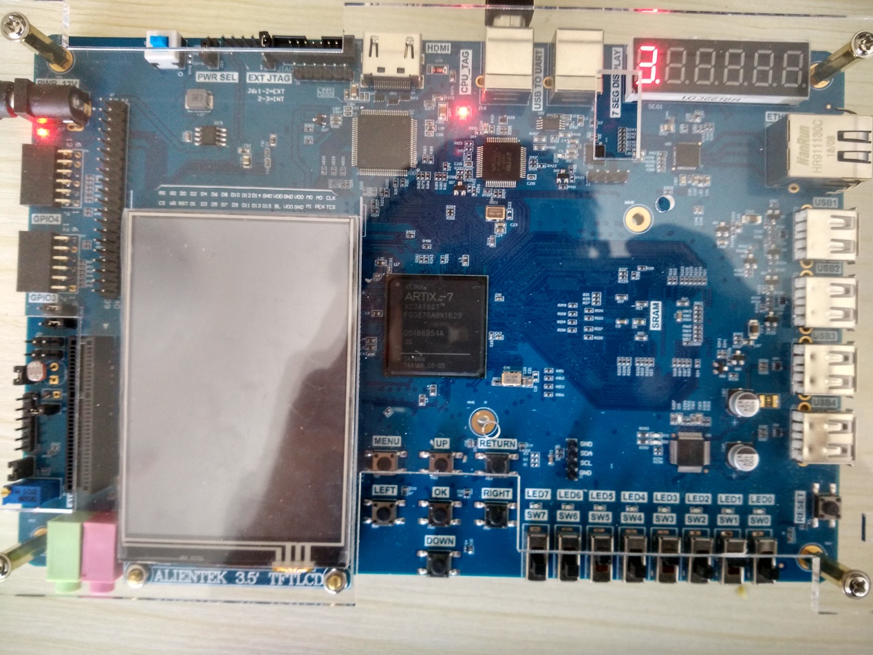
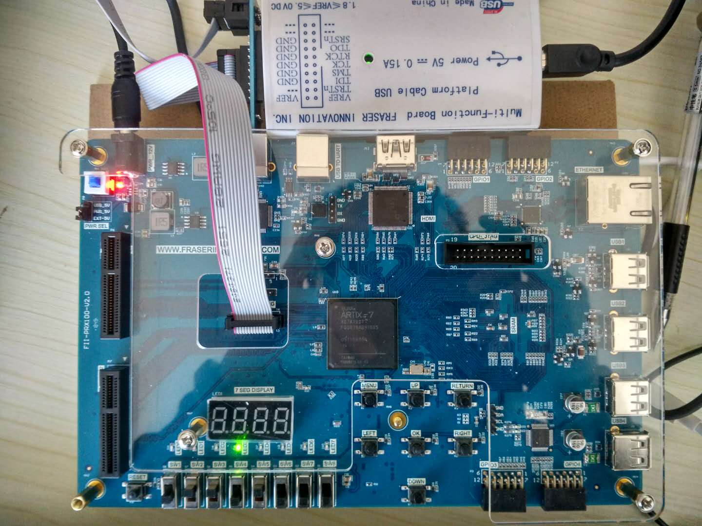
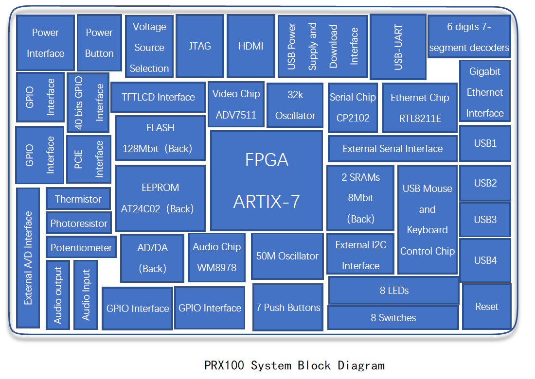
Xilinx Risc-V Board Tutorial : Basic Digital Clock Experiment and Programming of FPGA Configuration Files- FII-PRX100 FPGA Board Experiment 3
Experiment 3 Basic Digital Clock Experiment and Programming of FPGA Configuration Files 1.Experiment Objective Review the contents of experiment 1 and experiment 2, master the configuration of PLL, the design of frequency divider, the principle of schematics and the pin assignment of FPGA. Study BCD decoder Display design of 4-digit hexadecimal to 7 segment display decoders Generate a programmable configuration file and program it to the serial FLASH of the development board through the JTAG interface. 2.Design of The Experiment Refer experiment 1 for building new projects, chip selection module…
Read More


