Xilinx Risc-V Board Tutorial : Switches and Display – FII-PRX100 FPGA Board Experiment 2
Experiment 2 Switches and display
1.Experiment Objective
-
- Continue to practice using develop board
- Learn to use ILA (Integrated Logic Analyzer) in Vivado
- Learn to use the FPGA configuration memory for programming
2.Start New Project
-
- Refer to Experiment 1
- Select the same chip in Experiment 1
- Add PLL1 (Here PLL1 is optional, external input clock can be used directly)
3.Verilog HDL Code
| module SW_LED(
input inclk, input [7:0] sw, output reg[7:0] led ); wire sys_clk; wire pll_locked; reg sys_rst; always@(posedge sys_clk) sys_rst<=!pll_locked;
always @(posedge inclk) if(sys_rst) led<=8’hff; else led<=~sw; PLL1 PLL1_INST( .reset (1’b0), .clk_in1 (inclk), .clk_out1 (sys_clk), .locked (pll_locked) ); endmodule |
Schematics of develop board
-
- See Fig 2. 1. the diodes D19-D26 are mainly used to eliminate the damage of the FPGA pin caused by human body contact static electricity.

Fig 2. 1 Switches drive the circuit
4.FPGA Pin Assignment
| Signal Name | Port Description | Network Label | FPGA Pin |
| inclk | System Clock 50 MHz | C10_50MCLK | U22 |
| rst | Reset, high by default | KEY1 | M4 |
| led0 | LED 0 | LED0 | N17 |
| led1 | LED 1 | LED1 | M19 |
| led2 | LED 2 | LED2 | P16 |
| led3 | LED 3 | LED3 | N16 |
| led4 | LED 4 | LED4 | N19 |
| led5 | LED 5 | LED5 | P19 |
| led6 | LED 6 | LED6 | N24 |
| led7 | LED 7 | LED7 | N23 |
| SW0 | SW 0 | GPIO_DIP_SW0 | N22 |
| SW1 | SW 1 | GPIO_DIP_SW1 | L20 |
| SW2 | SW 2 | GPIO_DIP_SW2 | R16 |
| SW3 | SW 3 | GPIO_DIP_SW3 | P16 |
| SW4 | SW 4 | GPIO_DIP_SW4 | N17 |
| SW5 | SW 5 | GPIO_DIP_SW5 | R8 |
| SW6 | SW 6 | GPIO_DIP_SW6 | L17 |
| SW7 | SW 7 | GPIO_DIP_SW7 | L18 |
5.Program in Vivado
6.Download to the develop board to test and dial the DIP switch to see the corresponding LED light on and off. See Fig 2. 2.
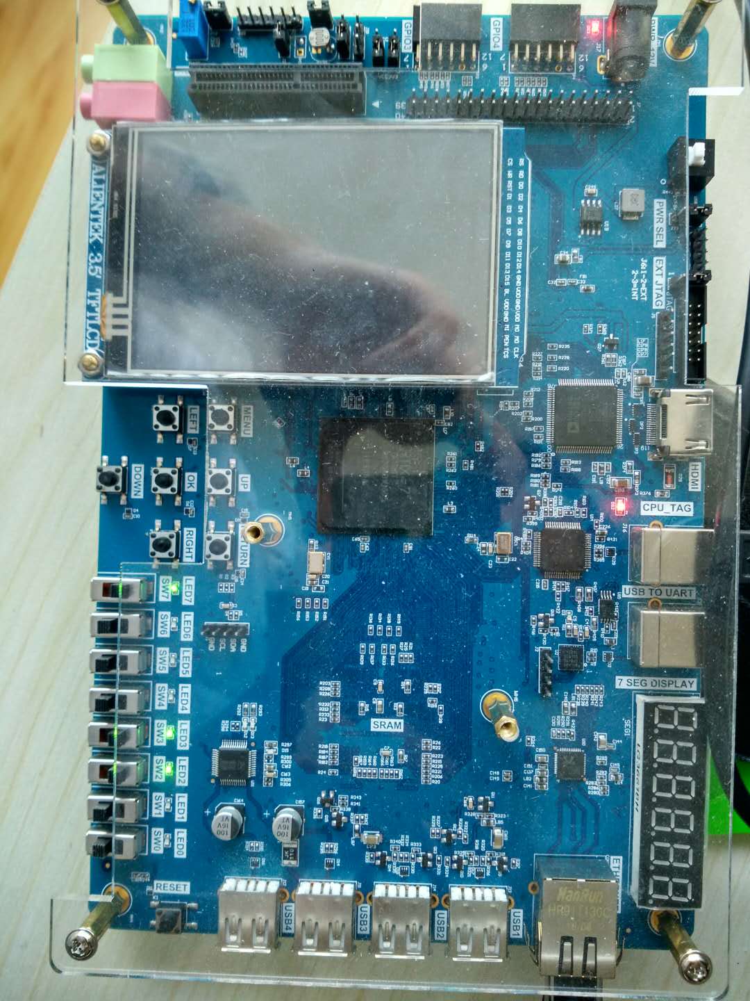
Fig 2. 2 Experiment result
7.Use of ILA
- Choose top-level entity SW_LED.v file to Run Synthesis
- After the integration is complete, under the Netlist window, all network nodes present in the current design are listed. Debug the network nodes. See Fig 2. 3.
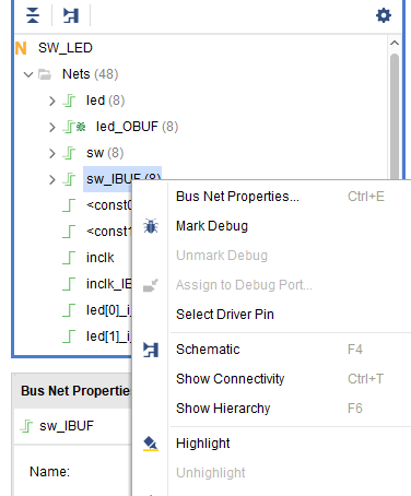
Fig 2. 3 Mark debugged network nodes
-
- In the Vivado main interface menu, execute the menu command Tool -> Set up Debug. In the popup window, there is clock domain of the selected debug signal. The clock domain of sw_IBUF is red. See Fig 2. 4.
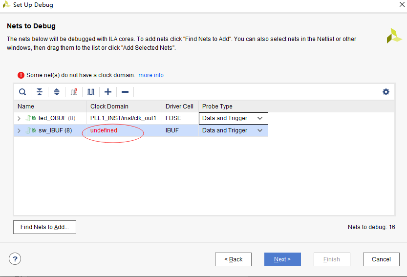
Fig 2. 4 Debugged network node clock domain setting
-
- In the red circle shown in Fig 2. 4, right click to set the clock domain.
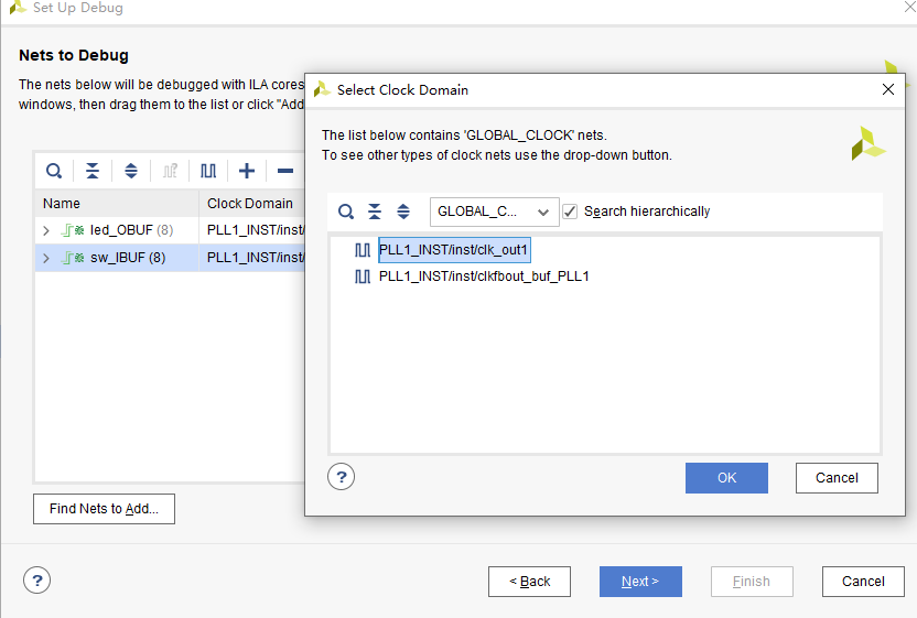
Fig 2. 5 Modify the debugged network node clock domain
-
- After the setting is completed, click Next. The popup window is shown in Fig 2. 6. Set the data collection depth and select the check box in front of Capture control and Advance trigger. Then keep clicking Next until the end.
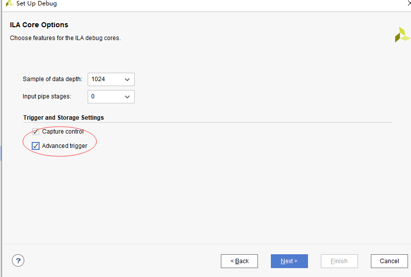
Fig 2. 6 Set the data collection depth
-
- Add I/O pin constraint information for implementation. Then generate a bit file and download it to FPGA. The debugging interface is automatically popped up. Click the icon button to see the following results. The test results in the debug diagram below Fig 2. 7 indicate that the design results are correct.
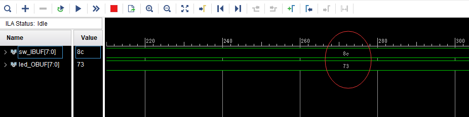
Fig 2. 7 Debug
When the input of switch is high, the input LED pin is controlled to be low, and the LED is lit. The figure for the experiment result on board from above shows that the input sw is 10001100 and the LED light is 01110011. The hexadecimal is 8c and 73 respectively. It is consistent with the ILA test results in the figure above.
- Modify the trigger condition to test the output under different trigger conditions