Xilinx Risc-V Board Tutorial : Basic Digital Clock Experiment and Programming of FPGA Configuration Files- FII-PRX100 FPGA Board Experiment 3
Experiment 3 Basic Digital Clock Experiment and Programming of FPGA Configuration Files
1.Experiment Objective
-
- Review the contents of experiment 1 and experiment 2, master the configuration of PLL, the design of frequency divider, the principle of schematics and the pin assignment of FPGA.
- Study BCD decoder
- Display design of 4-digit hexadecimal to 7 segment display decoders
- Generate a programmable configuration file and program it to the serial FLASH of the development board through the JTAG interface.
2.Design of The Experiment
-
- Refer experiment 1 for building new projects, chip selection
| module BCD_counter(
input rst, input inclk, //c0_50Mclk output reg [7:0] seven_seg, output reg [3:0] scan ); wire sys_clk; wire pll_locked; reg sys_rst; reg ext_rst;
always@(posedge sys_clk) begin sys_rst<=!pll_locked; ext_rst<=rst; end |
-
- Add PLL, the input clock is 50 MHz, and the output clock is 100 MHz. Refer experiment 1 for more information
| BCD_counterPLL1 BCD_counterPLL1_inst
( .areset(1’b0), .inclk0(inclk), .c0(sys_clk), .locked(pll_locked) ); |
-
- Add microsecond, millisecond, and second frequency dividers. Refer to experiment 1.
| reg [7:0] us_reg;
reg [9:0] ms_reg; reg [9:0] s_reg; reg us_f,ms_f,s_f,min_f;
always@(posedge sys_clk) //Microsecond frequency division if(sys_rst) begin us_reg<=0; us_f<=1’b0; end else begin us_f<=1’b0; if(us_reg==99)begin us_reg<=0; us_f<=1’b1; end else begin us_reg<=us_reg+1’b1; end end always@(posedge sys_clk) if(sys_rst) begin ms_reg<=0; ms_f<=1’b0; end else begin ms_f<=1’b0; if(us_f)begin if(ms_reg==999)begin ms_reg<=0; ms_f<=1’b1; end else ms_reg<=ms_reg+1’b1; end End always@(posedge sys_clk) if(sys_rst) begin s_reg<=0; s_f<=1’b0; end else begin s_f<=1’b0; if(ms_f)begin if(s_reg==999)begin s_reg<=0; s_f<=1’b1; end else s_reg<=s_reg+1’b1; end end |
-
- Minute and second frequency divider
| always@(posedge sys_clk) //Second frequency division
if(!ext_rst)begin counta<=0; countb<=0; min_f <=1’b0; end else begin min_f <=1’b0; if(s_f) begin if(counta==4’d9) begin counta<=4’d0; if(countb==5)begin countb<=0; min_f<=1’b1; end else countb<=countb+1’b1; end else begin counta<=counta+1’b1; end end end
always@(posedge sys_clk) //Minute frequency division if(!ext_rst)begin countc<=4’d0; countd<=4’d0; end else begin if(min_f) begin if(countc==4’d9) begin countc<=4’d0; if(countd==5)begin countd<=0; end else countd<=countd+1’b1; end else begin countc<=countc+1’b1; end end end |
-
- Learn the schematics of the common anode segement decoder and the connection between the scanning circuit and the FPGA.
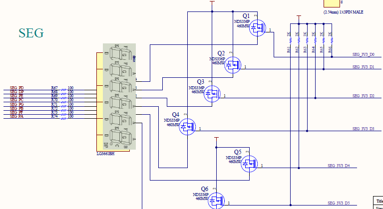
Fig 3. 1 Common anode segment decoder schematics
-
-
- The pins of segment display decoder are shown in Fig 3. 1. This is a schematic diagram of the six decoders combined. The pin names A, B, C, D, E, F, and G (corresponding connections are SEG_PA, SEG_PB, SEG_PC, SEG_PD, SEG_PE, SEG_PF, SEG_PG) correspond to the 7 segments of the decoder, and the DP (corresponding connection is SEG_PD)corresponds to the 8th segment, which is commonly used as a decimal point display.
-
A, B, C, D, E, F, G, D, P select which segment of the decoder will lit. The segment to be lit corresponds to the low point.
Illumination of segment decoders is controlled by the bit selection lines SEG_3V3_D0, SEG_3V3_D1, SEG_3V3_D2, SEG_3V3_D3, SEG_3V3_D4, SEG_3V3_D5.
-
-
- Code for the segment display decoder
-
| always@(*)
case(count_sel) 0:seven_seg_r<=7’b100_0000; 1:seven_seg_r<=7’b111_1001; 2:seven_seg_r<=7’b010_0100; 3:seven_seg_r<=7’b011_0000; 4:seven_seg_r<=7’b001_1001; 5:seven_seg_r<=7’b001_0010; 6:seven_seg_r<=7’b000_0011; 7:seven_seg_r<=7’b111_1000; 8:seven_seg_r<=7’b000_0000; 9:seven_seg_r<=7’b001_0000; default:seven_seg_r<=7’b100_0000; endcase always@(posedge sys_clk) seven_seg<={1’b1,seven_seg_r}; |
-
-
- Dynamic canning
-
The dynamic scanning of the segment display decoder utilizes the visual persistence characteristic of the human eye, and in addition to the speed of change that the human eye can distinguish, the segment corresponding to each decoder is quickly and time-divisionally illuminated. Because the time taken to illuminate all the decoders is less than the visual persistence of the human eye, in the eyes of the people, these decoders are continuously lit at the same time, and there is no feeling of flickering.
| reg [1:0] scan_st;
always@(posedge sys_clk) if(!ext_rst) begin scan <=4’b1111; count_sel <=4’d0; scan_st<=0; end else case(scan_st) 0:begin scan <=4’b1110; count_sel<=counta; if(ms_f) scan_st<=1; end 1:begin scan <=4’b1101; count_sel <=countb; if(ms_f) scan_st <=2; end 2:begin scan<=4’b1011; count_sel <=countc; if(ms_f) scan_st<=3; end 3:begin scan<=4’b0111; count_sel<=countd; if(ms_f) scan_st<=0; end default:scan_st<=0; endcase |
3.FPGA Pin Assignment
| Signal Name | Port Description | Network Label | FPGA Pin |
| inclk | System clock 50 MHz | C10_50MCLK | U22 |
| rst | Reset, high by default | KEY1 | M4 |
| seven_seg[0] | Segment a | SEG_PA | K26 |
| seven_seg[1] | Segment b | SEG_PB | M20 |
| seven_seg[2] | Segment c | SEG_PC | L20 |
| seven_seg[3] | Segment d | SEG_PD | N21 |
| seven_seg[4] | Segment e | SEG_PE | N22 |
| seven_seg[5] | Segment f | SEG_PF | P21 |
| seven_seg[6] | Segment g | SEG_PG | P23 |
| seven_seg[7] | Segment h | SEG_DP | P24 |
| scan[0] | Segment 1 | SEG_3V3_D0 | R16 |
| scan[1] | Segment 2 | SEG_3V3_D1 | R17 |
| scan[2] | Segment 3 | SEG_3V3_D2 | N18 |
| scan[3] | Segment 4 | SEG_3V3_D3 | K25 |
-
- Lock the pin, compile, and download the program to the develop board
- Observe the test result
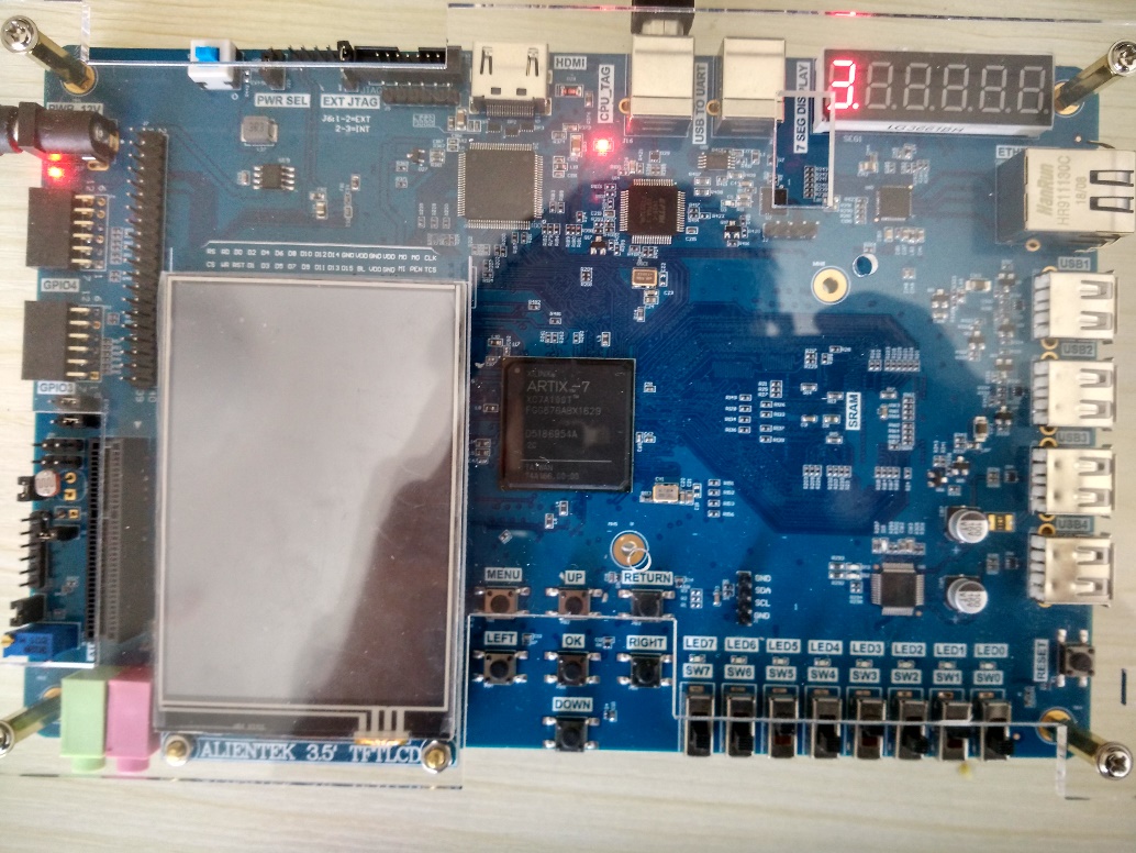
Fig 3. 2 Segment decoder illuminates
4.Configure the Serial Flash Programming
-
- The schematics of configuring serial Flash is as follows:
Figure 3. 3 Schematics of Serial Flash interface
-
- Configure FLASH and FPGA pin mapping
| FLASH | *SPI_CS_N | SPI_SO | *SPI_WP_N | SPI_IO | SPI_SCLK | *SPI_HOLD |
| FPGA PINS | P18 | R15 | P14 | R14 | M22 | N14 |
* SPI_CS_N, SPI_WP_N, SPI_HOLD must be connected to pull-up resistors
-
- FPGA configuration mode
-
- Configure the circuit, the resistor with the * mark in it is not soldered when the device is assembled, so the configuration circuit is selected as MSEL=0010, as shown in Table above.
Fig 3. 4 Configuration option
-
- Generate a readable configuration file
- See Fig 3. 5, right click on PROGRAM AND DEBUG to pop up the bitstream setting option.
- Generate a readable configuration file
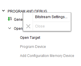
Fig 3. 5 Bit file generation setting
-
-
- Click Bitstream setting, tick bin_file*, click OK. See Fig 3. 6.
-
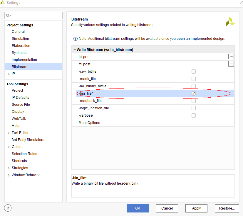
Fig 3. 6 Bin file generation setting
-
-
- See Fig 3. 7, click Generate Bitstream to generate the bit file and bin file. Click Open Hardware Manager to connect the board
-
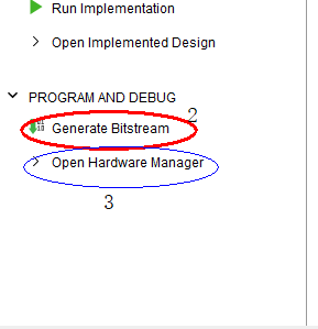
Fig 3. 7 Bit file generation
-
-
- Click Open target to connect with the board. See Fig 3. 8.
-
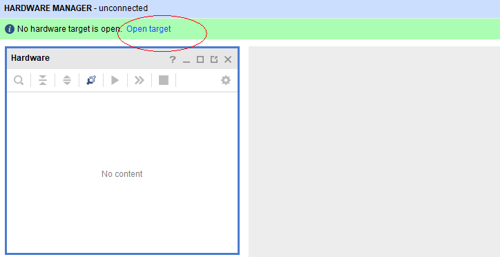
Fig 3. 8 Connect to the develop board
- Select the chip in step 1, right click to choose Add Configuration Memory Device in step 2. See Fig 3. 9.
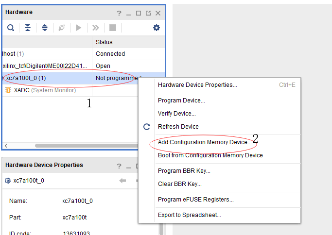
Fig 3. 9 Adding memory device
- Choose the Flash chip to be mt25ql128, then click OK. See Fig 3. 10.
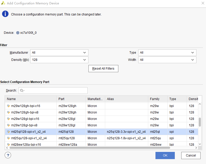
Fig 3. 10 Select Flash part
- Add bin file to be the Configuration file.
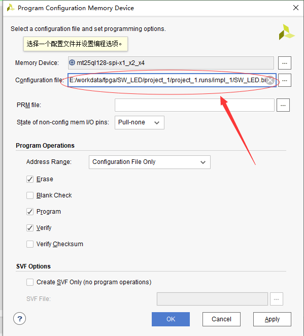
Fig 3. 11 Add the bin file
- The test result is shown in Fig 3. 12.

Fig 3. 12 Test result