xilinx Risc-V FPGA Board – FII-PRX100 – FPGA Development Board System Introduction
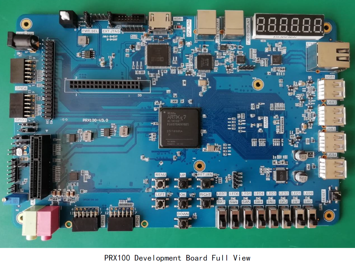
FII-PRX100 Development Board ( ARTIX 100T, XC7A100T, RISC-V FPGA Developing Board)

Online Shopping:
https://fpgamarketing.com/FII-PRX100-ARTIX-100T-XC7A100T-RISC-V-FPGA-Board-PRX100-1.htm
Fraser Innovation Inc develops FII-PRX100 based on the boards of the Xilinx ARTIX-7 series. It was initial released in 2018. This development board is resource-rich and high-speed, making it an ideal platform for learning and engineering research. This development board has been spent a lot on system design, PCB design, and function creation. It could even be said comprehensive and powerful.
System Design Objective
The main purpose of this system design is to complete FPGA learning, development and experiment with Xilin-Vivado. The main device uses the Xilinx-XC7A100T-2FGG676I and is currently the latest generation of FPGA devices from Xilinx. The main learning and development projects can be completed as follows:
- Basic FPGA design training
- Construction and training of the SOPC (Microblaze) system
- IC design and verification, the system provides hardware design, simulation and verification of RISC-V CPU
- Development and application based on RISC-V
- The system is specifically optimized for hardware design for RISC-V system applications
2. System Resource
- Extended memory
- Use two Super Srams in parallel to form a 32-bit data interface with a maximum access space of 2M bytes.
- IS61WV51216 (2 pieces) 512K x 32bit
- Serial flash
- Spi interface serial flash (128M bytes)
- Serial EEPROM
- Gigabit Ethernet: 100/1000 Mbps
- USB to serial interface: USB-UART bridge
3. Human-computer Interaction Interface
-
- 8 toggle switches
- 8 push buttons
- Definition of 7 push buttons: up, down, left, right, ok, menu, return
- 1 for rest: Reset button
- 8 LEDs
- 6 7-segment decoders
- I2C bus interface
- UART external interface
- Two JTAG programming interfaces
- One is for downloading the FPGA debug interface, and the other one is the JTAG debug interface for the RISC-V CPU
- Built-in RISC-V
- CPU software debugger, no external RISC-V JTAG emulator required
- 12-pin GIPIO connectors, in line with PMOD interface standards
4 Software Development System
-
- Vivado 18.1 and later version for FPGA development, Microblaze SOPC
- Freedom Studio-Win_x86_64 Software development for RISC-V CPU
5. Supporting Resources
-
- RISC-V JTAG Debugger
- xilinx Altera JTAG Download Debugger
- FII-PRX100 Development Guide
FII-PRX100 uses Xilinx’s ARTIX-7 series chip, model XC7A100T-2FGG676I, which is currently Xilinx’s latest generation FPGA device.
The Artix-7 is one of the Xilinx 28nn FPGA families. It features a small form factor package that reduces the power consumption of the Artix-7 family by half compared to the Spartan-6 family.
PRX100 system block diagram:
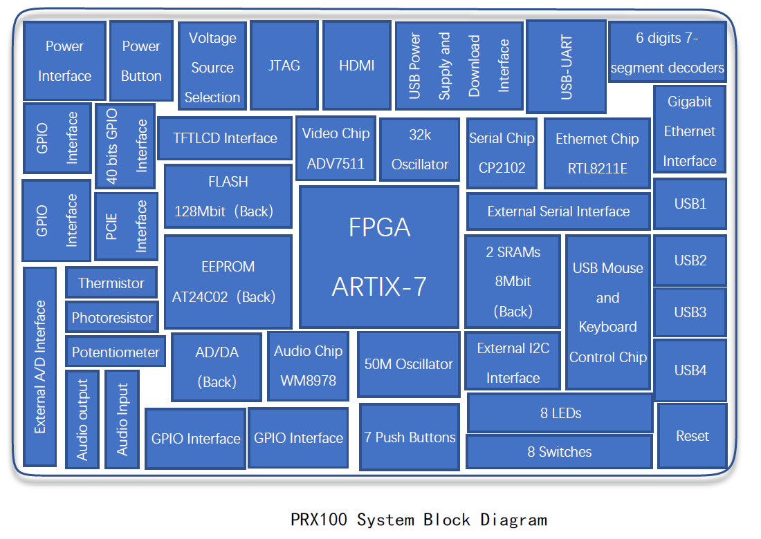
PRX100 Hardware resources:
- It can be powered by external 12V DC source or by “USB Power Supply and Download Interface”. The latter also provides program download functionality. Only one wire is to complete the power supply and download functions;
- A 50 MHz oscillator, a 32.768 kHz oscillator, provides a stable clock source for the development board;
- 6-digit common anode 7-segment decoders, through dynamic scanning to achieve data display;
- 1 HDMI interface displaying color pictures or camera video;
- 1 chip I2C interface EEPROM chip, model AT24C02;
- 1 adaptive 10 M/100M/Gigabit Ethernet interface;
- 8 push buttons, 7 for programmable buttons, 1 for reset button;
- 1 photoresistor, through which it can simulate light control; 1 thermistor, which can collect temperature or analog temperature alarm function; 1 potentiometer, which can simulate voltage change;
- 1 PCF8591 AD/DA conversion chip, reserved external interface, free input and output;
- Onboard 50MHz and 32.768kHz oscillators provide stable clock signals to the development board;
- 8-bit DIP switch;
- 8-bit LED;
- 1 128Mbit Flash chip;
- 4 GPIO external signal expansion interfaces, also the PMOD standard interface;
- A 40-pin GPIO expansion interface that provides a large amount of I/O for developers to use freely;
- Two JTAG interfaces, one for the FPGA download debug interface (J4, J5) and one for the RISC-V CPU JTAG debug interface(J16). Built-in RISC-V CPU software debugger, no external RISC-V JTAG emulator required;
- 1 UART asynchronous serial interface;
- 2 SRAMs with a capacity of 8Mbit;
- a pair of audio input and output interfaces;
- 1 PCIE interface;
- 4 USB interfaces, 2 for the mouse and keyboard interface, 2 for the universal serial interface;
- 1 USB (USB-B) to UART interface for serial communication;
- 1 TFTLCD touch screen interface, which can realize the display and operation of the touch screen;