Verilog HDL program to achieve frequency division, Write Verilog HDL program to implement LED shifting – Risc-V FPGA Board Xilinx – Development Board Experiment 1 – LED Shifting – FII-PRX100
Experiment 1 LED Shifting
- Practice how to use the development system software Vivado to establish a new project, call the system resource PLL to establish the clock.
- Write Verilog HDL program to achieve frequency division
- Write Verilog HDL program to implement LED shifting
- Combine hardware resources for FPGA pin configuration
- Compile
- Download the program to the develop board
- Observe the experimental result and debug the project
2. Create A New Project Under Vivado
- Start Vivado in the start Menu. See Fig 1. 1
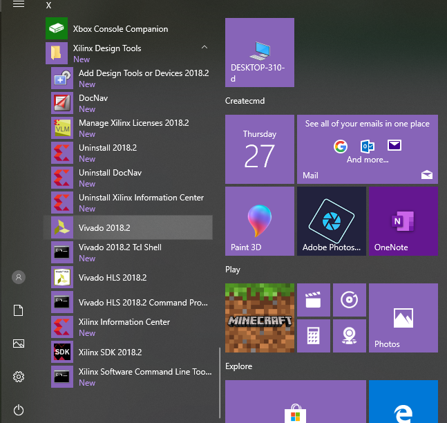
Fig 1. 1 Start Menu
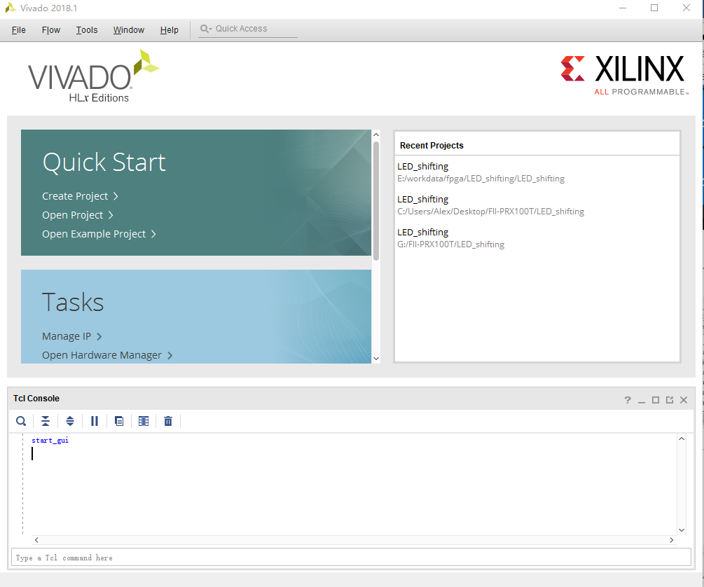
Fig 1. 2 Initial interface of Vivado
- File -> Project -> NEW
- Click the Next option button in the pop-up dialog box. Then pop up the setup project interface of Fig 1. 3 and Fig 1. 4
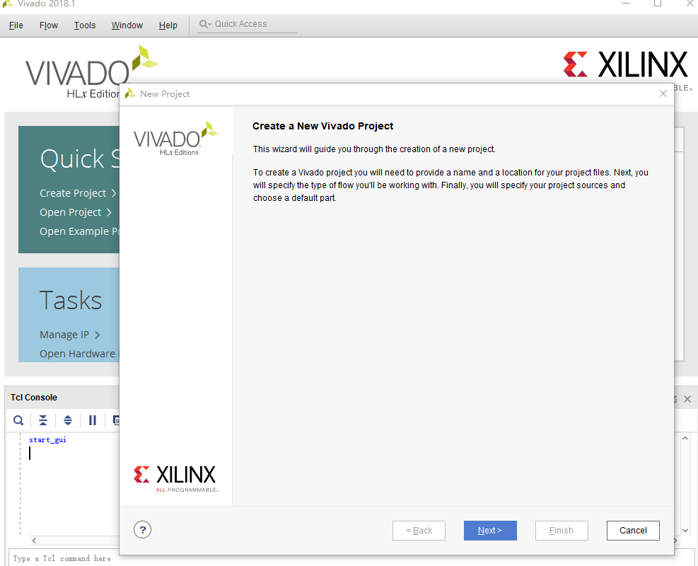
Fig 1. 3 Create a new project
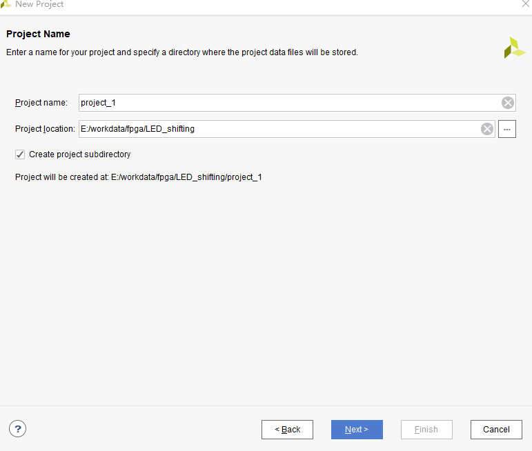
Fig 1. 4 Set the project path
Set the project name, project path. Note that the top-level file name must be consistent with the file name of the subsequent top-level file of Verilog. The top-level file name is case-sensitive.
-
- Choose RTL Project to be the project type. See Fig 1. 5.
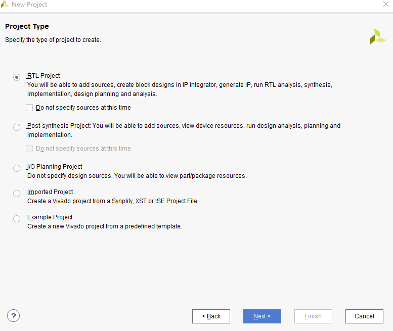
Fig 1. 5 Project type selecting
-
- Click Next as shown in Fig 1. 6 (there is no source file that can be added since it is new)
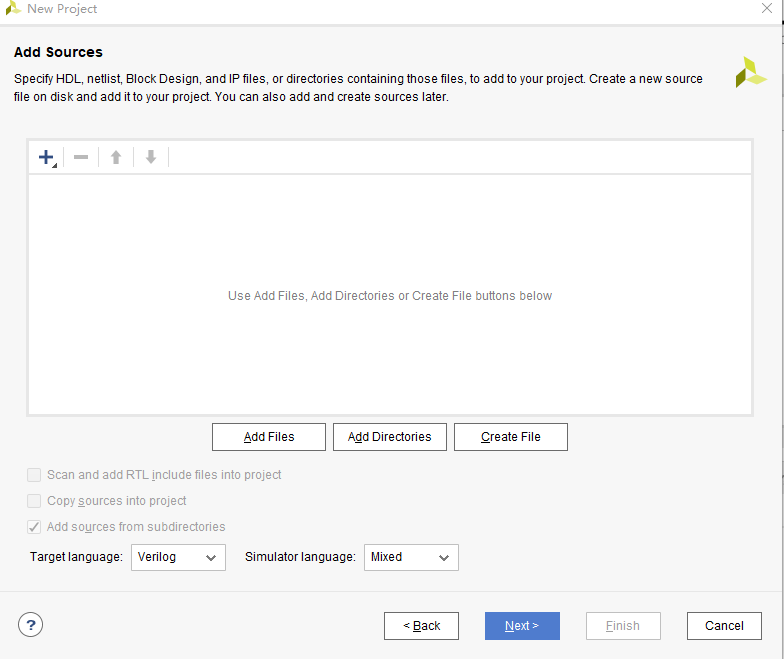
Fig 1. 6 Add source file
-
- Click Next as shown in Fig 1. 7 (there are no files that can be added to constrain due to it is a new project)
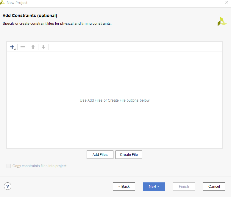
Fig 1. 7 Add constrains
-
- Select XC7A100TFGG676-2 in the selection dialog box. See Fig 1. 8, click NEXT, then Finish to complete the project building.
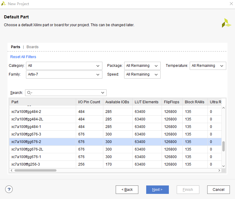
Fig 1. 8 Choose the default Xilinx part or board
- Create a Verilog HDL file, LED_shifting.v
- Select File -> Add Sources or add the RTL file as shown in Fig 1. 9 or Fig 1. 10 below.

Fig 1. 9 Add source file
Fig 1. 10 Add source file
-
- See Fig 1. 11, select Add or create design sources and then click Next.
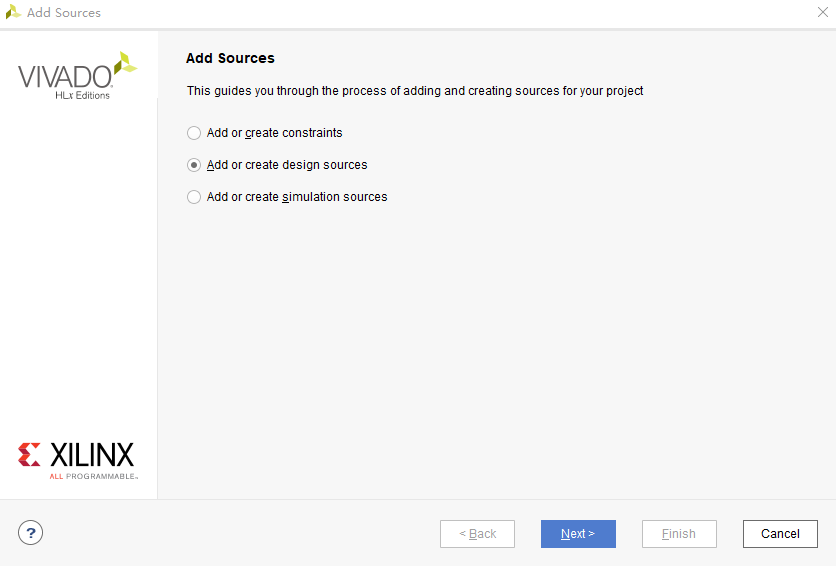
Fig 1. 11 Add source file 1
-
- Click Create File. In the popup window, select the Verilog HDL for the file type. Fill in the file name and location -> OK -> Finish. See Fig 1. 12.
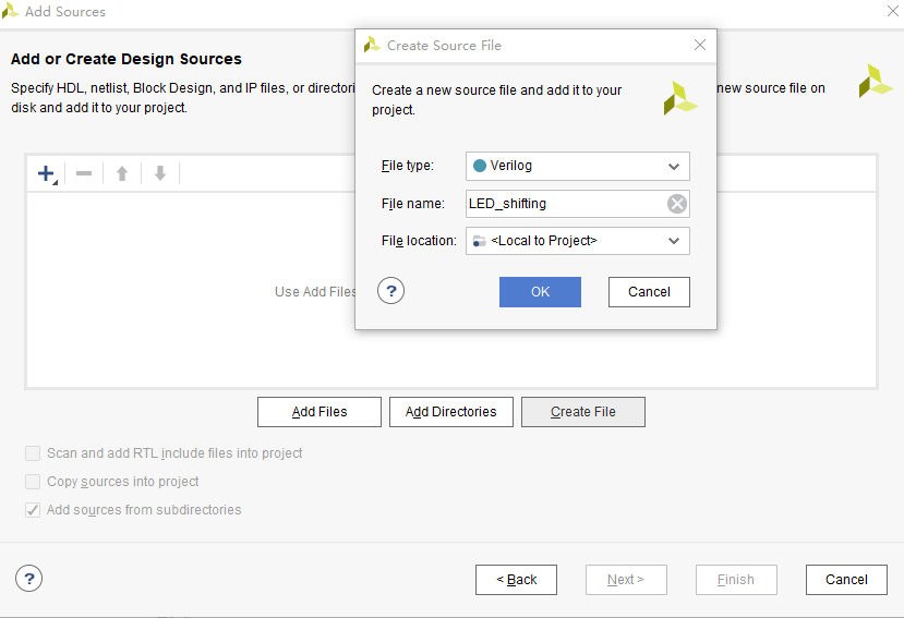
Fig 1. 12 Add source file 2
-
- As shown in Fig 1. 13, if filling the module name wrongly in the previous step, the name can be modified here. Input and output pin configuration can also be directly set here through the I/O port definitions. (You can also write the generated pin information in the Verilog code later.) Then click OK.
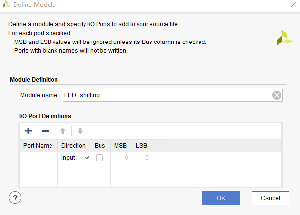
Fig 1. 13 Confirmation
-
- Vivado’s sources window generates an LED_shifting RTL file. Click on the file to edit the code. See Fig 1. 14.
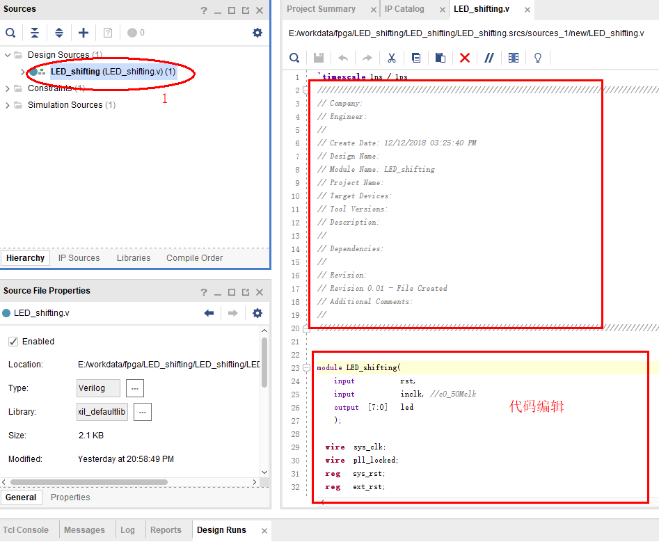
Fig 1. 14 Source file editing
-
- Edit interface file
module Led_shifting(
input rst,
input inclk, //c0_50Mclk
output [7:0] led
);
endmodule
- Add clock module
See Fig 1. 15, click the IP Catalog option on the left side of the main interface to pop up the corresponding core supported by the engineering chip. Find the needed IP core by functions or names, or by fast searching. Entering clocking in step 1, then click Clocking Wizard shown in step 2. The clock IP configuration interface will appear after that.
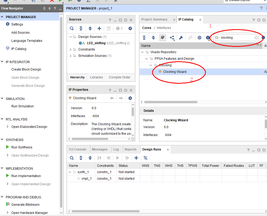
Fig 1. 15 PLL IP core setting
-
-
- Enter the clock setting as shown below
- Select either MMCM or PLL here. Here is an example of selecting a PLL core.
- The path filled in Fig 1. 16 is the setting of the clock file path. Fig 1. 17 shows the name setting.
- See Fig 1. 18, clk_in1 (which is the input clock of the PLL, where there is only one input clock) is set to be 50 MHz, which is consistent with the clock provided by the hardware board.
- Other PLL settings can be selected by default. If the required functions involve advanced features, use the official reference for more.
- Click the Output Clocks tab to set the PLL compensation output clock to clk_out1.
- For PLL asynchronous reset control and capture lock status settings, use the default mode shown in the figure.
- Enter the clock setting as shown below
-
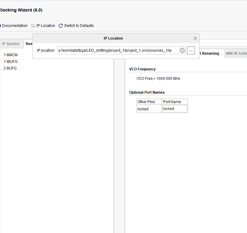
Fig 1. 16 IP location setting window
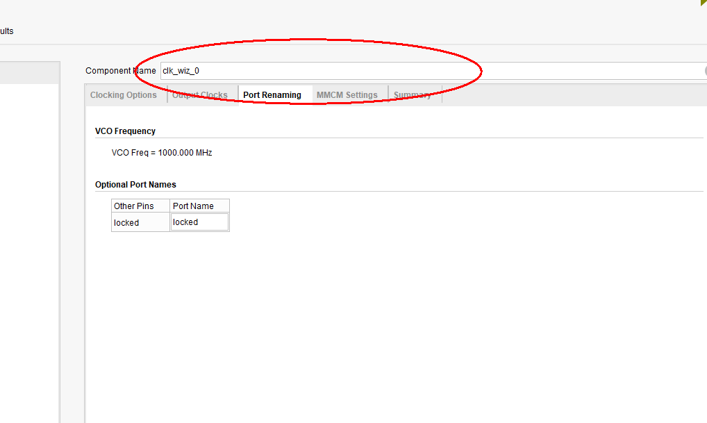
Fig 1. 17 IP core name setting
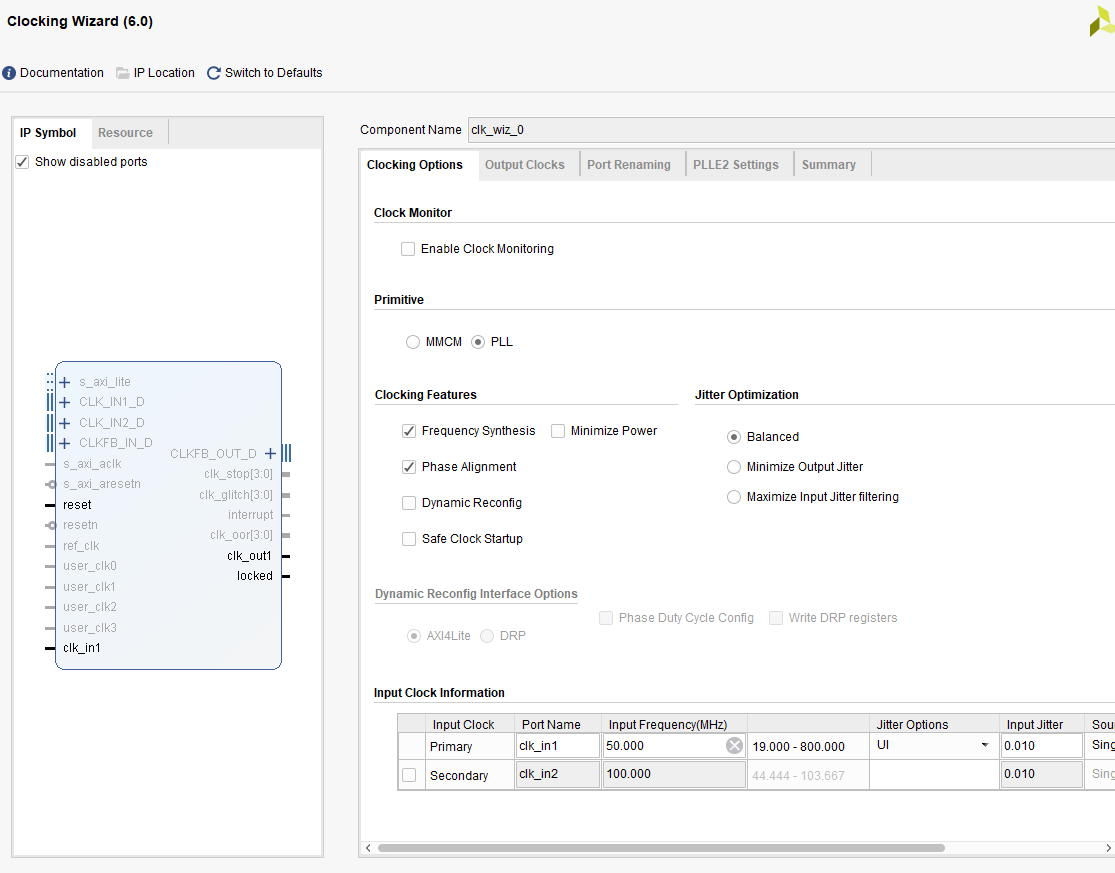
Fig 1. 18 PLL input clock setting
-
-
-
- See Fig 1. 19, set the output frequency to 100 MHz, the phase offset to 0, and the duty cycle to 50%. Click OK.
-
-
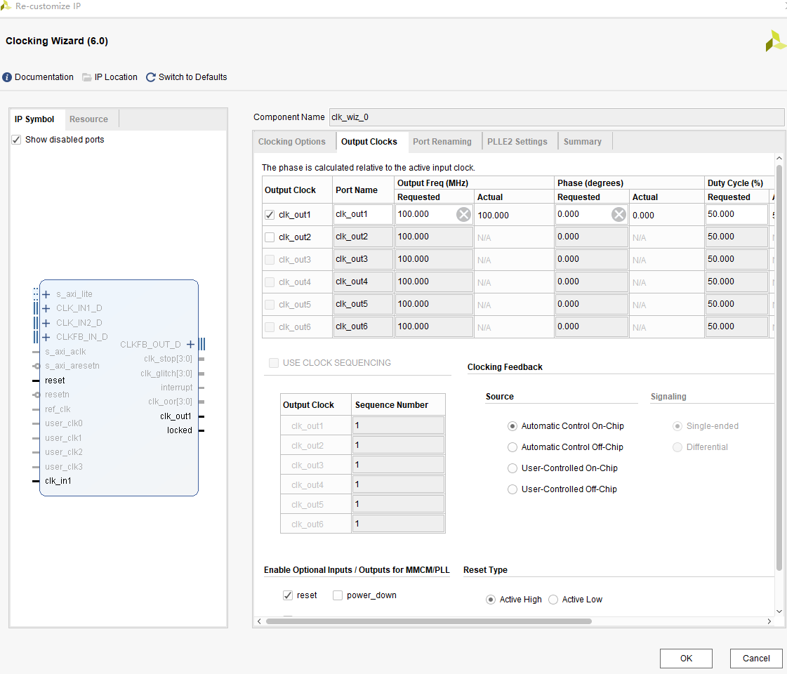
Fig 1. 19 Output frequency and duty cycle setting
-
-
-
- Click Generate to finish the IP core setting. See Fig 1. 20.
-
-
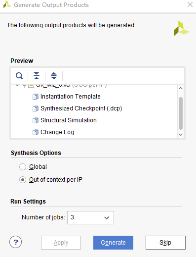
Fig 1. 20 Generate IP core
-
-
-
- After the clock module is generated, select the IP Sources sub-tab in the Labels box of the Sources of the project interface, that is, the IP core file can be found just after the generation. See Fig 1. 21.
- Instantiate the module to the top-level entity
-
-
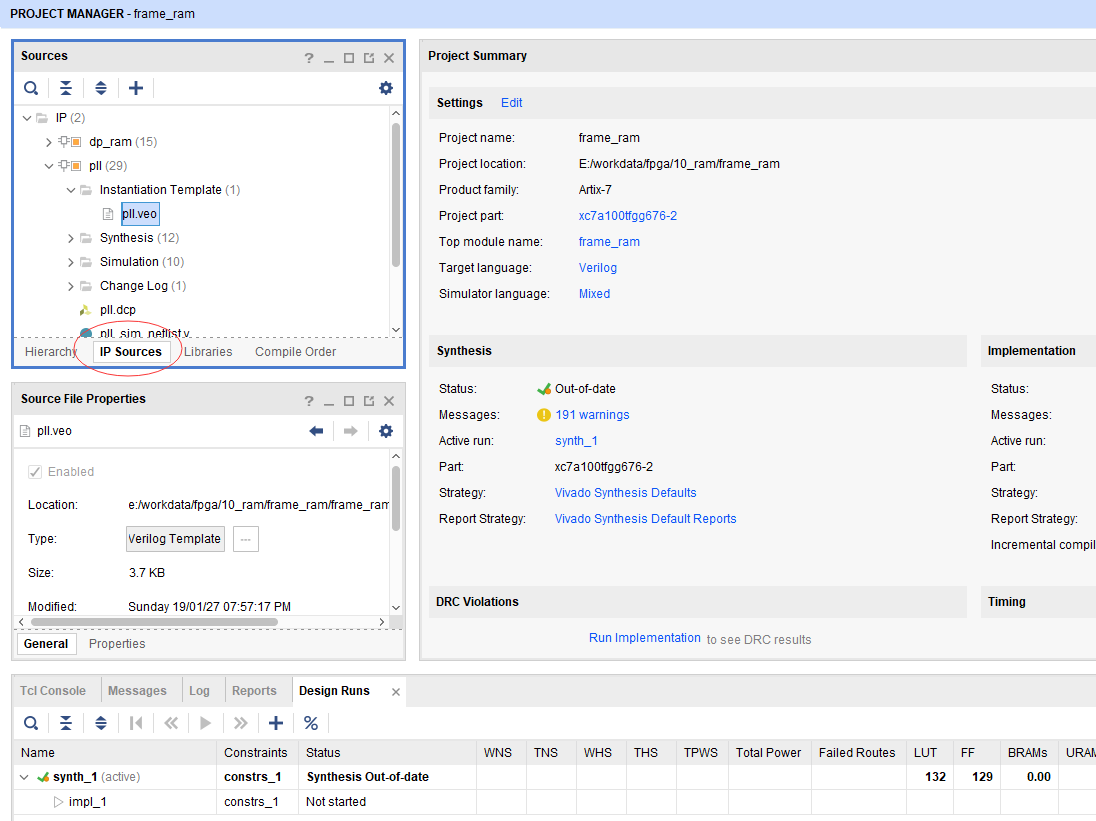
Fig 1. 21 Instantiate to the top-level entity
The code is as follows:
-
-
-
- Top-level entity instance
- Key signal description
-
-
sys_rst, the value before the PLL lock is ‘1’ as a reset signal for the entire system. After the system is locked (pll_locked == 1’b1), the value of sys_rst becomes ‘0’. At the same time, it is driven by the rising edge of sys_clk, so it is a synchronous reset signal.
| module Led_shifting(
input inclk, //c0_50Mclk output [7:0] led );
wire sys_clk; wire pll_locked; reg sys_rst;
always@(posedge sys_clk) begin sys_rst<=!pll_locked; end
clk_wiz_0 clk_wiz_0_inst( .clk_out1 (sys_clk), .reset (1’b0), .locked (pll_locked), .clk_in1 (inclk) ); endmodule |
Note that the user is already familiar with the Verilog syntax by default, so the Verilog syntax is not exhaustive here.
- Frequency division design
-
- The system clock is 100 MHz, while the speed of the LED blinking is set to be 1 second, so frequency division is needed.
- Microsecond frequency division
-
The Verilog HDL code is as follows:
| reg [7:0] us_reg;
reg us_f; always@(posedge sys_clk) if(sys_rst) begin us_reg<=0; us_f<=1’b0; end else begin us_f<=1’b0; if(us_reg==99)begin us_reg<=0; us_f<=1’b1; //Microsecond pulse, outputs a sys_clk pulse every //1 us end else begin us_reg<=us_reg+1; end end |
-
-
- Millisecond frequency division
-
| reg [9:0] ms_reg;
reg ms_f; always@(posedge sys_clk) if(sys_rst) begin ms_reg<=0; ms_f<=1’b0; end else begin ms_f<=1’b0; if(us_f) begin if(ms_reg==999)begin //Every 1000 microseconds, ms_f //produces a sys_clk pulse ms_reg<=0; ms_f<=1’b1; end else//Counter adds 1 every microsecond ms_reg<=ms_reg+1; end end |
-
-
- Second frequency division
-
| always@(posedge sys_clk)
if(sys_rst) begin s_reg<=0; s_f<=1’b0; end else begin s_f<=1’b0; if(ms_f) begin if(s_reg==999)begin s_reg<=0; s_f<=1’b1; end else s_reg<=s_reg+1; end end |
-
-
- LED shifting design
-
| always@(posedge sys_clk)
if(sys_rst) begin s_reg<=0; s_f<=1’b0; end else begin s_f<=1’b0; if(ms_f) begin if(s_reg==999)begin s_reg<=0; s_f<=1’b1; end else s_reg<=s_reg+1; end end |
Because the schematics design uses FPGA I/O sink current mode, it must be inverted bitwise before output. Otherwise, it will show that each time 7 LEDs are lit, only one LED is left in the non-lighting state.
Assign led=~led_r; //Bitwise inverse
The pin assignment table of the program is as follows:
| Signal Name | Port Description | Network Label | FPGA Pin |
| inclk | System clock 50 MHz | C10_50MCLK | U22 |
| rst | Reset, high by default | KEY1 | M4 |
| led0 | LED 0 | LED0 | N17 |
| led1 | LED 1 | LED1 | M19 |
| led2 | LED 2 | LED2 | P16 |
| led3 | LED 3 | LED3 | N16 |
| led4 | LED 4 | LED4 | N19 |
| led5 | LED 5 | LED5 | P19 |
| led6 | LED 6 | LED6 | N24 |
| led7 | LED 7 | LED7 | N23 |

Fig 1. 22 Schematics for LED
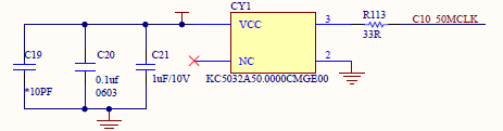
Fig 1. 23 FPGA input clock
- After the code is integrated, there are two ways to add the constraint file. One is to use the I/O planning function in Vivado, and the other is to directly create a constraint file for the XDC and manually enter the constraint command. Here the first method is adopted for now, I/O planning function. The procedure is as follows
-
- Go to Flow Navigator -> Synthesis -> Run Synthesis, integrate the project first. See Fig 1. 24. The purpose is:
- Check the syntax error
- Form the tree hierarchy of the project
- Go to Flow Navigator -> Synthesis -> Run Synthesis, integrate the project first. See Fig 1. 24. The purpose is:
-
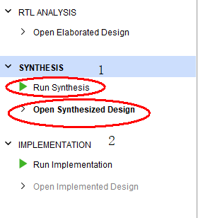
Fig 1. 24 Check the syntax, compilation synthesis
After the integration is complete, select Open Synthesized Design, open the comprehensive results, select I/O Planning under layout, and assign the pins in the I/O port section in the figure below.
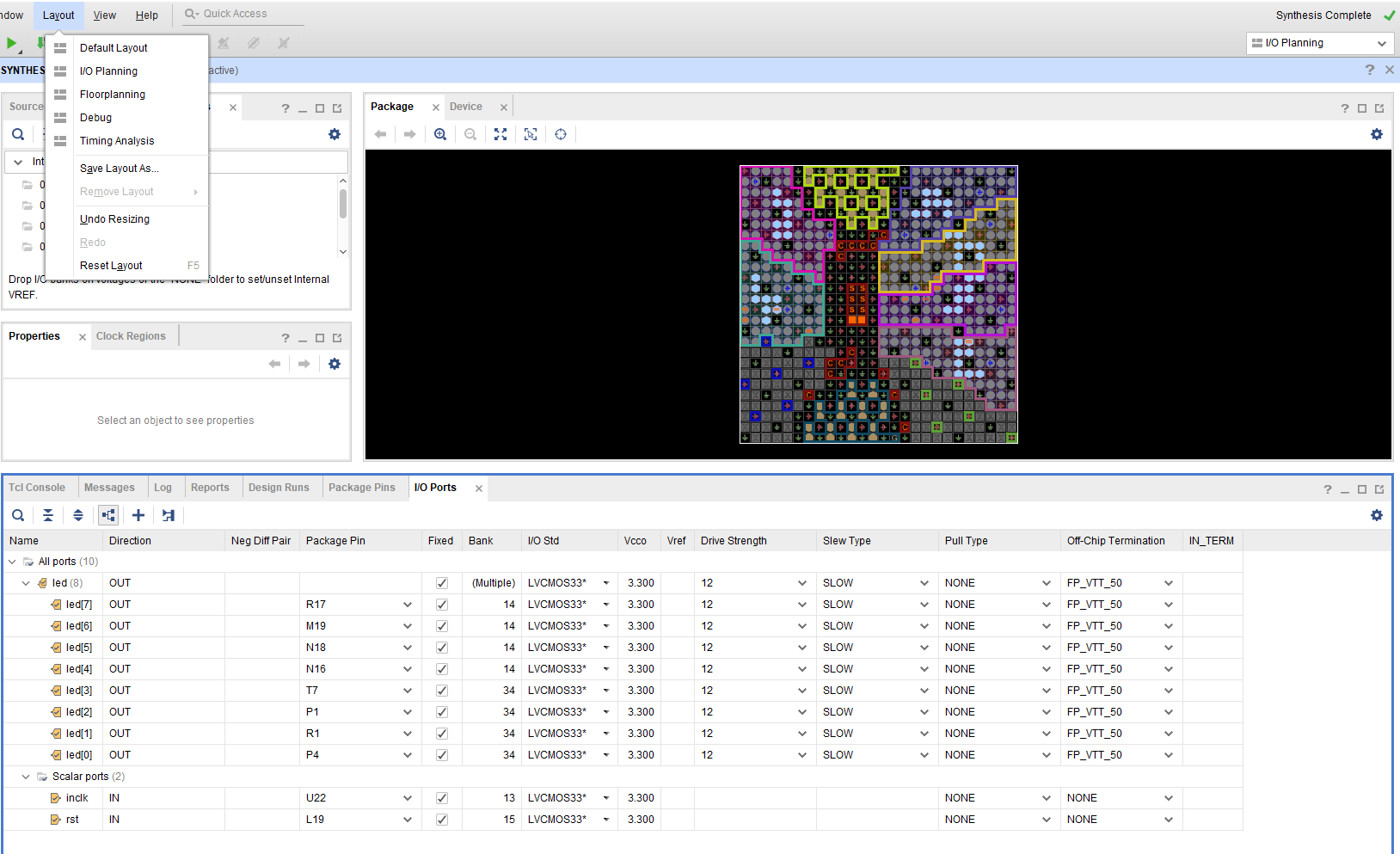
Fig 1. 25 Pin assignment
-
- After the pin assignment is completed, click Run Implementation as shown in Fig 1. 26. After the completion of the Generate Bitstream, generate a downloadable bit file. Click Open Hardware Manager to link to the device. See Fig 1. 27.
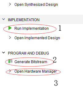
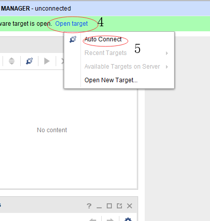
Fig 1. 26 Generate bit files Fig 1. 27 Connect with the experiment board
-
- As shown in Fig 1. 28 below, select the correct bit file and download the bit file settings.
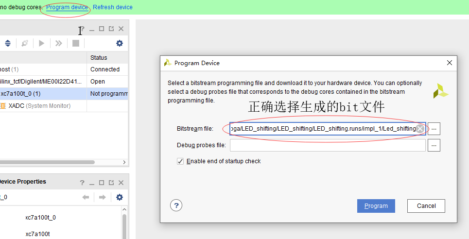
Fig 1. 28 Download the bit file configuration
-
- Click Program to download the program to the board to test
-
- The hardware connection is shown as follows, the 8 LEDs blink one by one.
-
- Click Program to download the program to the board to test
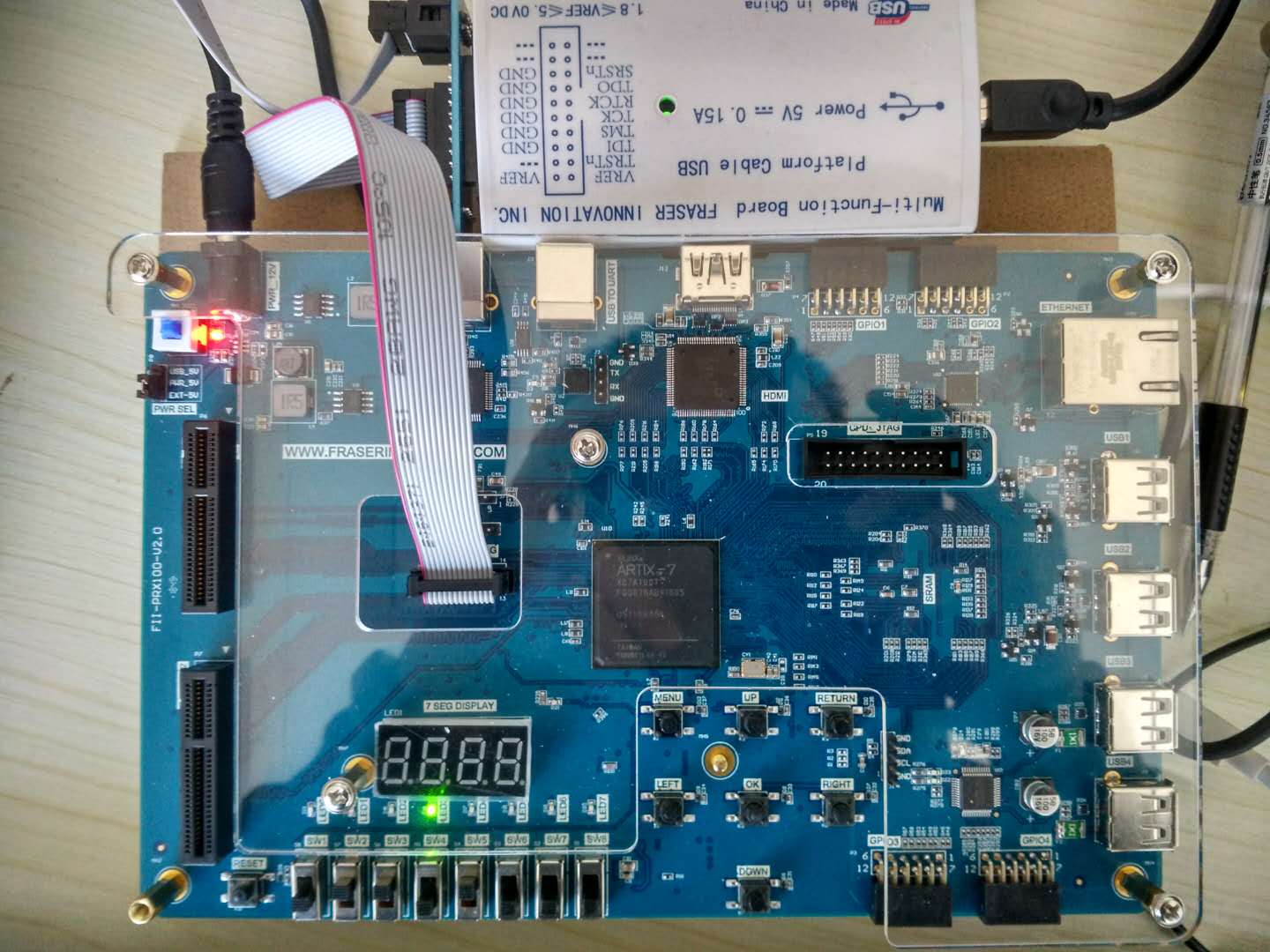
Fig 1. 29 Develop board
-
-
-
- Review the above steps to be proficient in each process
-
-
Exp