Learn to use ILA (Integrated Logic Analyzer) in Vivado, Practice the call of system resource PLL, zynq xc7z030 board – FII-PE7030 Experiment 2
Experiment 2 Analysis of Switch Signals via ILA
2.1 Experiment Objective
- Continue to practice using develop board
- Continue to practice the call of system resource PLL
- Learn to use ILA (Integrated Logic Analyzer) in Vivado
2.2 Experiment Implement
Capture and analyze switch signals on the development board by using ILA
2.3 Experiment
2.3.1 Introduction of Switches
The on-board switch is 8 DIP switches, as shown in Figure 2.1. The switch is used to switch the circuit by turning the switch handle.
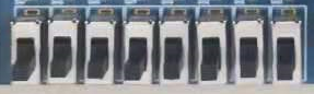
Figure 2.1 Switch physical picture
2.3.2 Hardware Design
The schematics of the switch is shown in Figure 2.2. One end of the 8-bit switch is connected to the VCC1V5_ALL terminal at the same time, which is at a high level. One end is respectively connected to an LED, and is connected to the control terminal SW_LED of the connected LED. When the DIP switch is selected, the FET is turned on at a high level, the LED is on, and a high-level signal is input to the FPGA at the same time. At this time, the LED will act as a switch strobe indication signal, and will light up when strobe.
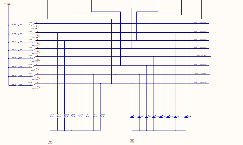
Figure 2.2 Schematics of the switches
2.3.3 Program Design
The first step: the establishment of the main program framework (interface design)
| module SW_LED(
input inclk_p, input inclk_n, input [7:0] sw, output reg [7:0] led );; endmodule |
The input signals for this experiment are differential clock signals inclk_p and inclk_n, 8-bit switch sw, and 8-bit led lights as output signals.
The second step: design content
| wire sys_clk;
wire pll_locked; reg sys_rst; clk_wiz_0 clk_wiz_0_inst( .clk_in1_p (inclk_p), .clk_in1_n (inclk_n), .reset (1’b0), .locked (pll_locked), .clk_out1 (sys_clk) ); always @ (posedge sys_clk) sys_rst <= !pll_locked; always @ (posedge sys_clk) begin if (sys_rst) led <= 8’d0; else led <= ~sw; end |
When the reset signal is valid, all 8 LEDs are off. After the reset is completed, the on/off of the LED is controlled by the switch, and the LED is on when the switch is on. (Due to hardware design reasons, LEDs are temporarily assigned to the segment display when constraints are added.)
2.4 Experiment Verification
(Refer to Experiment 1 for the board verification process in subsequent tests, which will not be described in detail)
The first step: add constraints and assign pins
The pin assignments are shown in Table 2.1.
Table 2-1 Switch and display experiment pin mapping table
| Signal Name | Network Name | FPGA Pin | Port Description |
| inclk_p | SYSCLK_P | AC13 | Input clock (differential)
200MHz |
| inclk_n | SYSCLK_N | AD13 | |
| sw[0] | GPIO_DIP_SW0 | A17 | 8-bit switch |
| sw[1] | GPIO_DIP_SW1 | E8 | |
| sw[2] | GPIO_DIP_SW2 | C6 | |
| sw[3] | GPIO_DIP_SW3 | B9 | |
| sw[4] | GPIO_DIP_SW4 | B6 | |
| sw[5] | GPIO_DIP_SW5 | H6 | |
| sw[6] | GPIO_DIP_SW6 | H7 | |
| sw[7] | GPIO_DIP_SW7 | G9 | |
| led[0] | SEF_PA | J10 | 8-bit LED
(segment display) |
| led[1] | SEF_PB | J9 | |
| led[2] | SEF_PC | A7 | |
| led[3] | SEF_PD | B7 | |
| led[4] | SEF_PE | A8 | |
| led[5] | SEF_PF | A9 | |
| led[6] | SEF_PG | A10 | |
| led[7] | SEF_DP | B10 |
The second step: run the implementation, generate bitstream files, and verify the board
After successfully downloading the generated programmable bitstream file to the Zynq_7030 development board, the experimental phenomenon is shown in Figure 2.3. Toggle the switch and the corresponding LED lights up.
2.5 Use of ILA
Design synthesis and adding constraints have been completed during the board verification. Therefore, expand the SYNTHESIS option under the Flow Nvigator window on the left side of the Vivado main interface, click Open Synthesized Design, and in the Sources window, click Netlist to open the netlist structure generated after the synthesis. All network nodes are under the Nets folder, as shown in Figure 2.4.
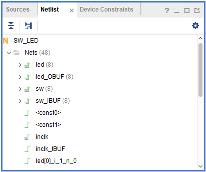
Figure 2.4 Netlist
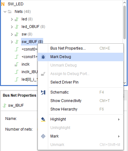
Figure 2.5 Mark network nodes to be debugged
As shown in Figure 2.5, right-click the network node to be debugged, and a floating command window appears. Click Mark Debug to mark the target network node. After all signals that need to be adjusted are marked (this experiment needs to debug the switch signal sw and the LED light signal led), click Tools on the Vivado menu bar, run the Set Up Debug command, and the Set Up Debug dialog box pops up, as shown in Figure 2.6.
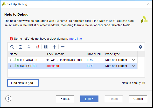
Figure 2.6 Set Up Debug dialog box
In Figure 2.6, all marked network nodes are in the window. Some signals need to manually add the clock domain. like sw_IBUF in this experiment. Clock Domain is displayed as red undefined. Right-click the network node without the clock, such as shown in Figure 2.7, the floating command dialog box pops up. Click the Select Clock Domain command to pop up the dialog box. As shown in Figure 2.8, select the 100MHz clock output by the PLL as the clock of the sw network node, and click the OK button. The clock is successfully added. Click the Next button in the Set Up Debug dialog box.
As shown in Figure 2.9, in the following settings, the Sample of data depth is set according to actual needs. For this experiment, the default value is 1024. For the input pipe stages, the default value is 0. Under the Trigger and Storage Settings option, check the Capture control and Advanced trigger options, click the Next button, and click the Finish button in the pop-up dialog box to complete the debugging settings.
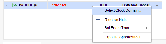
Figure 2.7 Adding a clock domain
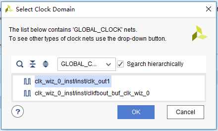
Figure 2.8 Selecting the clock
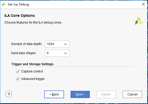
Figure 2.9 Other debugging settings
After completing the debugging and setting, refer to Experiment 1, re-run the design synthesis, run the implementation, and generate the bitstream file (the project without added constraints needs to add additional constraint files), and then program the board. After success, the Vivado interface will automatically jump to the debugging interface, as shown in Figure 2.10.
Expand led and sw. At this time, the 8-bit switches are all 0 and unselected. The LEDs are all 1 and off. As shown in Figure 2.11.
Set the trigger condition to sw! = 8’h00, and click to run ILA, as shown in Figure 2.12.
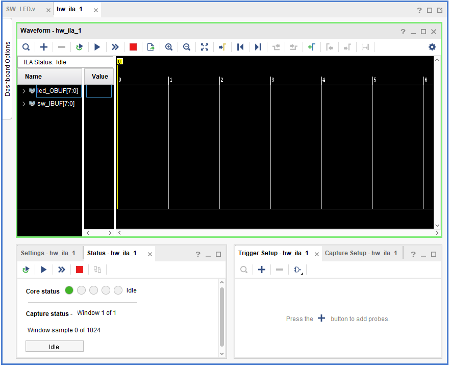
Figure 2.10 ILA debugging interface
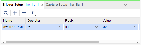
Figure 2.11 Set trigger conditions
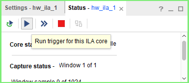
Figure 2.12 Running ILA
Pull up the first bit switch sw [1], as shown in Figure 2.13. At the position shown by the T red line, the left side is the previous state, and the right side is the post-trigger state. When the trigger condition is met, sw [1] changes from 0 to 1, switch 1 is on, and at the same time, led [1] changes from 1 to 0. The LED 1 is on, corresponding to the FII-PRA100T development board at this time, which is in line with the debugging results.
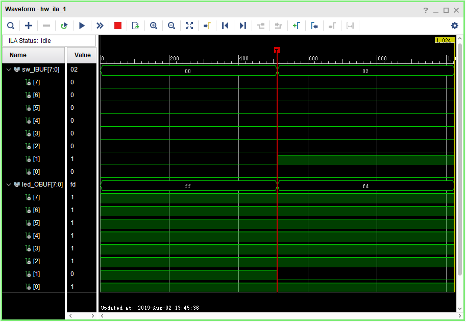
Figure 2.13 Debugging results
Set different trigger conditions, observe and analyze the experimental results.