EVB Board – Basic FPGA design training – FII-PE7030 User Experimental Manuals
Version Control
| Version | Date | Description |
| V1.0 | 21/11/2019 | Initial Release |
Contents
Part One: Introduction to Zynq_7030 Development System 5
3、Human-computer Interaction Interface 5
4、Software Development System 6
Part Two: zynq_7030 Main Resources Usage and FPGA Development Experiemnt 8
Experiment 1 LED Shifting Design 9
1.4 Experiment Verification 26
Experiment 2 Analysis of Switch Signals via ILA 32
2.3.1 Introduction of Switches 32
2.4 Experiment Verification 34
Experiment 3 Segment Display Digital Clock Experiment 41
3.3.1 Introduction to Segment Display Decoder 41
3.4 Experiment Verification 47
Experiment 5 Button Debounce 49
4.3.1 Introduction to Button and Debounce Principle 49
4.4 Experiment Verification 55
Experiment 5 Digital Clock Comprehensive Experiment 58
5.4 Experiment Verification 62
Experiment 6 Use of Multipliers and ISIM 64
6.4 Compile and Call of ISIM Simulation and Modelsim Simulation Library 67
Experiment 7 Hexadecimal Number to BCD Code Conversion and Application 72
7.2.1 Introduction to Hexadecimal Number to BCD Code Conversion 72
7.4 Application of Hexadecimal Number to BCD Code Conversion 76
7.5 Experiment Verification 77
8.4 Experiment Verification 83
Experiment 9 Use Dual-port RAM to Read and Write Frame Data 84
9.4 Experiment Verification 93
9.5 Experiment Summary and Reflection 94
Experiment 10 Asynchronous Serial Port Design and Experiment 96
10.3.1 USB to Serial Chip (FT2232) Introduction 96
10.3.3 Program Introduction 97
10.4 Experiment Verification 102
Experiment 11 IIC Protocol Transmission 104
11.3.1 Introduction to EEPROM and IIC Protocol 104
11.3.2 Hardware Introduction 105
11.3.3 Program Introduction 106
11.4 Experiment Verification 119
Experiment 12 HDMI Experiment 121
13.3.1 Introduction to HDMI Interface and ADV7511 Chip 121
13.3.3 Program Introduction 122
13.4 Experiment Verification 129
13.3.1 Introduction to Experiment Principle 132
14.3.3 Program Introduction 135
13.4 Experiment Verification 154
Part One: Introduction to Zynq_7030 Development System
1、System Design Objective
The main purpose of this system design is to complete FPGA learning, development and experiment with Xilin-Vivado. The main device uses the XC7Z030-1FFG676C. The main learning and development projects can be completed as follows:
(1)Basic FPGA design training
(2)Construction and training of the SOPC (Microblaze) system
(3)IC design and verification, the system provides hardware design, simulation and verification of RISC-V CPU.
(4)Based on RISC-V development and application.
(5)The system is specifically optimized for hardware design for RISC-V system applications.
2、System Resource
- Extended memory: two DDR3 (PL end) four DDR3 (PS end)
- 32M serial FLASH memory
- Serial EEPROM
- Gigabit Ethernet (one for PS end and one for PL end)
- USB to serial interface: USB-UART bridge
3、Human-computer Interaction Interface
- 8-bit DIP switches
- A total of 8 push buttons, 7 of which are defined as (MENU, UP, RETUN, LEFT, OK, RIGHT, DOWN), one push button is defined as FPGA hardware reset (RESET)
- 8-bit LED
- 6 7-segment display
- I2C bus interface
- Two JTAG programming interfaces: one for the FPGA download debug interface, one for the RISC-V CPU JTAG debug interface
- Built-in RISC-V CPU software debugger, no external RISC-V JTAG emulator required
- One 12-pin GPIO connector, in line with PMOD interface standard
4、Software Development System
- Vivado 18.1 and later version for FPGA development, Microblaze SOPC
- Freedom Studio-Win_x86_64 Software development for RISC-V CPU
5、Supporting Resources
RISC-V JTAG Debugger
Xilinx JTAG Download Debugger
FII-PE7030 PE7030 Harware Reference Guide
FII-PE7030 PE7030 User Experimental Manual
6、Physical Display
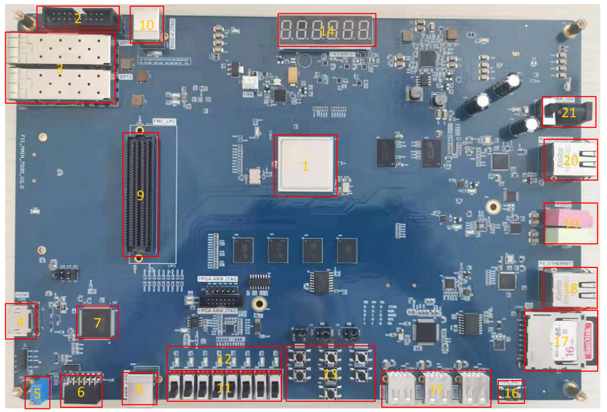
Figure 1 FII-PE7030 physical picture
Corresponding to the physical picture, the main components of the development board are as follows:
1:ZYNQ_7030 chip
2:RISCV_JTAG download port
3:Fiber interface
4:HDMI interface
5:Potentiometer
6:GPIO interface
7:HDMI chip (ADV7511)
8:FPGA download port
9:FMC interface
10:RISC-V download port
11:8-bit DIP switch
12:8-bit LED
13:7 push buttons
14:6 seven-segment display
15:USB interface
16:reset button (RESET)
17:SD card
18:Ethernet interface (PS end)
19:Audio output (green) and audio input (red)
20:Ethernet interface (PL end)
21:External 12V power connector
Part Two: zynq_7030 Main Resources Usage and FPGA Development Experiemnt
This part mainly guides the user to learn the development of FPGA program and the use of onboard hardware through the development example of FPGA. At the same time, the application system software Xilinx is introduced from the elementary to the profound. The development exercises covered in this section are as follows:
Experiment 1: LED shifting design
Experiment 2: ILA experiment
Experiment 3: Segment display digital clock experiment
Experiment 4: button debouncing experiment
Experiment 5: digital clock comprehensive experiment
Experiment 6: use of multiplier and ISIM simulation
Experiment 7: hex to BCD conversion and application
Experiment 8: usage of ROM
Experiment 9: use dual-RAM to read and write frame data
Experiment 10: asynchrounous serial port design and experiment
Experiment 11: IIC transmission experiment
Experiment 12: HDMI experiment
Experiment 13: Ethernet experiment
Experiment 1 LED Shifting Design
1.1 Experiment Objective
- Practice how to use the development system software Vivado to establish a new project, call the system resource PLL to establish the clock.
- Write Verilog HDL program to achieve frequency division and implement LED shifting
- Combine hardware resources for FPGA pin configuration
- Compile, download the program to the develop board, and verify
- Observe the experimental result and debug the project
1.2 Experiment Implement
- All LEDs light up during reset;
- After reset, LED lights from low to high (from right to left) in turn;
- Each LED is lit for one second;
- After the last (highest position) LED is lit, the next time it returns to the first (lowest position) LED, the loop is achieved;
1.3 Experiment
1.3.1 LED Introduction
LED (Light-Emitting Diode), is characterized by low operating current, high reliability and long life. Up to now, there are many types of LED lights, as shown in Figure 1.1. The FII-PE7030 uses the LED lights in the red circle.
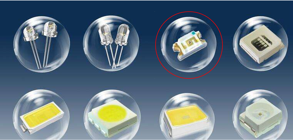
Figure 1.1 Different kinds of LEDs
1.3.2 Hardware Design
The physical picture of the onboard 8-bit LED is shown in Figure 1.2. The schematics of LED is shown in Figure 1.3. The LED module of this experiment board adopts 8 common anode LEDs, which are connected with Vcc 5V through 510 R resistors, and the negative electrode is grounded through the N-channel field effect transistor (FET), the gate of the FET is grounded through a 4.7K resistor, and the FPGA is connected to the gate of the FET through the GPIO_DIP_SW terminal.When the FPGA outputs a high level of 1, a current flows through the LED, and it is turned on.

Figure 1.2 8-bit LED physical picture
Figure 1.3 Schematics of LED
1.3.3 Program Design
1.3.3.1 Start Program
Before writing a program, let’s briefly introduce the development environment we use and how to create a project. Take Vivado 18.2 as an example. The specific project establishment steps are shown in Figure 1.4 to 1.9.
The first step: open the Vivado 2018.2 integrated development environment

Figure 1.4 Vivado development environment
The secodn step: under the Quick Start group in the main interface of the Vivado 2018.2, click the Create Project option to bring up the Create a New Vivado Project dialog box. Click Next to bring up the Project Name dialog box. In Figure 1.5, determine the project name and project location. Take this experiment as an example, set the parameters according to the figure.
Figure 1.5 New Project-Project Name dialog box
The third step: click the Next button in Figure 1.5 to bring up the Project Type dialog box, as shown in Figure 1.6.
Figure 1.6 New Project-Project Type dialog box
- Choose RTL Project
- Check Do not specify sources at this time
The fourth step: click the Next button in Figure 1.6 to bring up the Default Part dialog.
In order to speed up the search for the device, as shown in Figure 1.7, set the parameters according to the figure.
- Category:ALL
- Family:Zynq_7000
- Package:ffg676
- Speed:-1
- Temperature:All Remaining
The window shown in Figure 1.7 lists the devices available for selection. In this design, the device model number is xc7z030ffg676-1.
The fifth step: click the Next button in Figure 1.7 to bring up the New Project Summary dialog box, as shown in Figure 1.8. This dialog box explains the type, name, and device information of the new project.
The sixth step: click the Finish button in Figure 1.8 to complete the creation of the new project.
After the creation is successful, Vivado automatically transfers to the PROJECT MANAGER interface, as shown in Figure 1.9, for developers to proceed to the next step.
Figure 1.7 Default Part dialog box
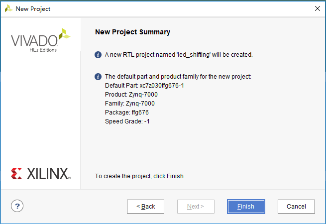
Figure 1.8 New Project Summary dialog box
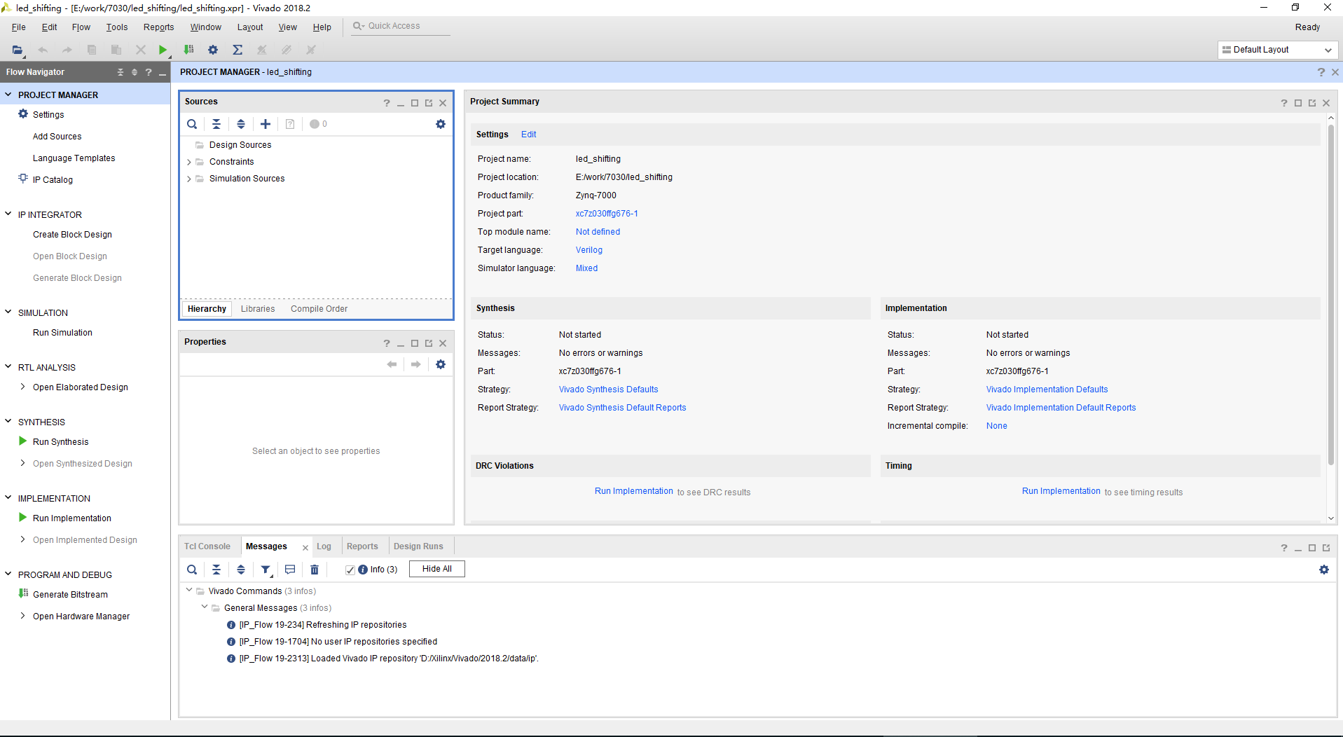
Figure 1.9 PROJECT MANAGER interface
1.3.3.2 Create and Add a New Design File
After the new project is created, continue to create the file (Verilog HDL file). The steps are as follows.
The first step: select the Design Sources folder under the Sources window, click the icon ╋ in the window, or click the right mouse button to bring up the floating menu, execute the Add Sources command, and Add Sources dialog box pops up. As shown in Figure 1.10, select Add or create design sources.
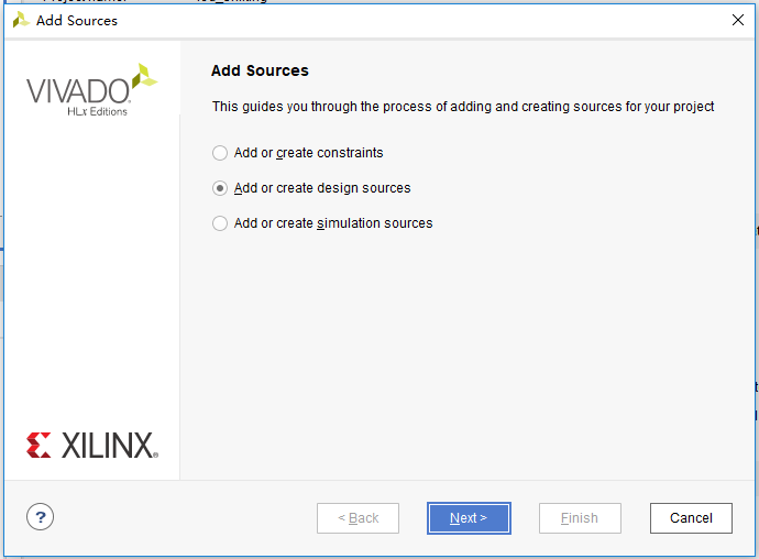
Figure 1.10 Add Sources dialog box
The second step: click the Next button in Figure 1.10 to bring up the Add or Create Design Sources dialog box, as shown in Figure 1.11.
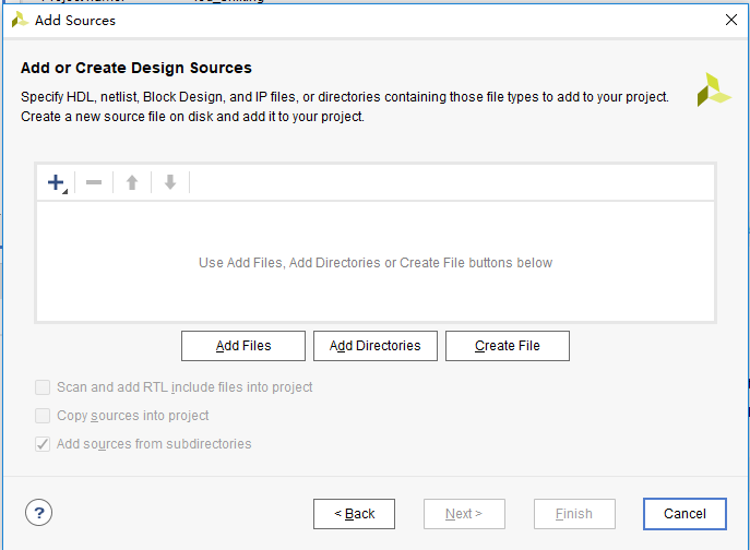
Figure 1.11 Add or Create Design Sources dialog box
The third step: click the Create File button in Figure 1.11; or click the icon ╋, the floating menu appears, select the Create File.
The fourth step: the Create Source File dialog box pops up, as shown in Figure 1.12.
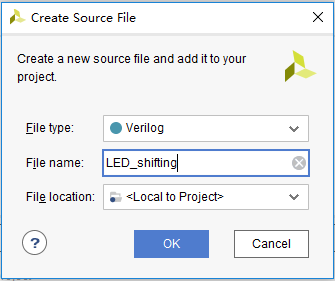
Figure 1.12 Create Source File dialog box
In the dialog box, set the file type and file name as follows.
- File type:Verilog
- File name:LED_shifting
- File location:Local to Project
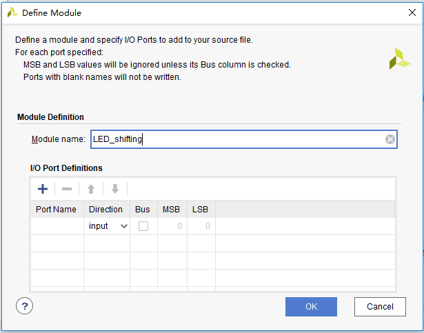
Figure 1.13 Define Module dialog box
The fifth step: click the OK button in Figure 1.12 to exit the Create Source File dialog.
The sixth step: add the LED_shifting.v file to the dialog shown in Figure 1.11.
The seventh step: click the Finish button in Figure 1.11 to bring up the Define Module dialog box, as shown in Figure 1.13.
In the Define Module dialog box, the port of the module can be defined, or in the later design file. This design directly defines the port in the Define Module dialog box. The input signal of the design are clock signal (differential clock) and external hardware reset signal, the output signal are 8 LEDs. Set the parameters according to the figure shown below. The setting result is shown in Figure 1.14.
- For clock signal, Port Name:inclk_p;Direction:input;
Port Name:inclk_n;Direction:input;
- For external reset signal, Port Name:rst;Direction:input;
- For 8-bit LED signal, Port Name: led; Direction: output; check the Bus option, set MSB to 7, and LSB to 0.
The eighth step: click the OK button to complete the creation of the design file. As shown in Figure 1.15, the LED_shifting.v file is added under the Design Sources folder in the Sources window.
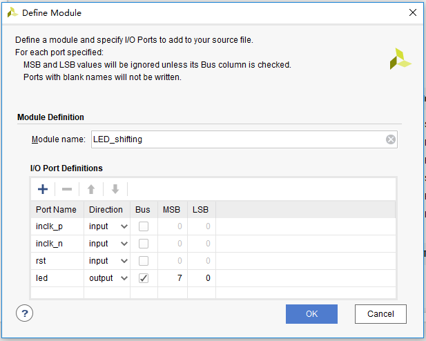
Figure 1.14 Define Module dialog box (for port difinition)
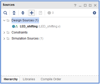
Figure 1.15 Add LED_shifting.v file
The ninth step: double-click the LED_shifting.v file to open the design file, as shown in Figure 1.16.
Figure 1.16 Design file interface
The tenth step: in the module of the design file, design and write the code. (If the module port is not defined in the Define Module dialog box, the design file is opened as shown in Figure 1.17 and needs to be defined here.)
Figure 1.17 Design file interface when the port is not defined in advance
1.3.3.3 Introduction to the Program
The first step: the establishment of the main program framework (port design)
| module LED_shifting(
input inclk_p, input inclk_n, input rst, output reg [7:0] led ); endmodule |
The input signals of this experiment have differential clock signals inclk_p and inclk_n, reset signal rst, and output signal 8-bit LED, which is defined by the bus form of led [7:0].
The second step: IP core invoking
In this experiment, a 100MHz clock is required as the operating clock of the following frequency division module, and the onboard input clock is a 200MHz differential clock, so the PLL frequency division is used to obtain a 100Mhz clock. Steps as follows.
- In the Flow Navigator on the left side of the Vivado main interface, select and expand the PORJECT MANAGER option to find the IP Catalog option, as shown in Figure 1.18.
Figure 1.18 IP core
Figure 1.19 IP core content window
- Click IP Catalog, and the interface will pop up on the right side of the main interface. The IP addresses available in vIvado are in this directory, as shown in Figure 1.19.
- Use search to quickly find the IP core to use, enter clocking in the search bar, and the available clock IP core resources appear below, as shown in Figure 1.20, select the Clocking Wizard option.
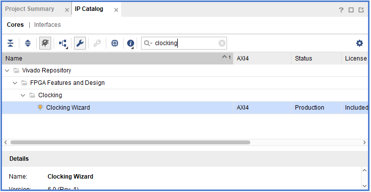
Figure 1.20 Searching for the target IP core
- Double-click the Clocking Wizard to bring up the Customize IP dialog box, as shown in Figure 1.21, set it according to the following parameters.
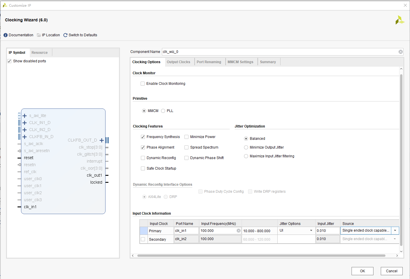
Figure 1.21 PLL setting interface
- In the Primitive interface, select the PLL, as shown in Figure 1.22.
- In the Clocking Options interface, the primary clock in the Input Clock Information dialog box, Input Frequency: 200; Source: Differential clock capable pin (the input clock is a differential clock with a frequency of 200MHz), as shown in Figure 1.23.
- In the Output Clocks interface, the output clock clk_out1, Output Freq: 100, Phase: 0, Duty Cycle: 50 (output clock is 100MHz, phase offset is 0, duty cycle is 50%) as shown in Figure 1.24.

Figure 1.22 Choose PLL
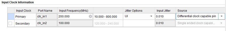
Figure 1.23 PLL Input Clock Settings
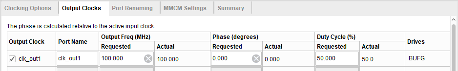
Figure 1.24 PLL output Clock Settings
- Click the OK button to complete the setup and the Generate Output Products dialog box will pop up. As shown in Figure 1.25.
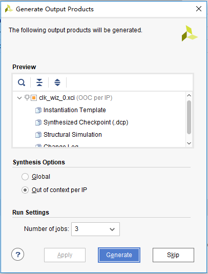
Figure 1.25 Generate Output Products dialog box
- Click the Generate button to generate the PLL.
In the Sources window of the main interface, click the IP Sources column, click the IP core PLL in the IP folder, expand the Instantiation Template, as shown in Figure 1.26, there is a PLL instantiation template file PLL.veo.
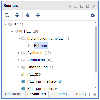
Figure 1.26 Generate an instantiation template for the PLL
The third step: instantiate the PLL into the design file
| wire sys_clk;
wire pll_locked; clk_wiz_0 clk_wiz_0_inst( .clk_in1_p (inclk_p), .clk_in1_n (inclk_n), .reset (1’b0), .locked (pll_locked), .clk_out1 (sys_clk) ); |
When the system is powered on, the locked signal has a value of 0 before the PLL locks (stable operation). locked is high after the PLL locks, and the clock signal sys_clk outputs normally.
The fourth step: determine the reset signal
sys_rst is used as the reset signal of the frequency division part, and ext_rst is used as the reset signal of the shifting LEDs. It is driven by the rising edge of the clock sys_clk, it is synchronously reset by the primary register.
| reg sys_rst;
reg ext_rst; always @ (posedge sys_clk) begin sys_rst <= !pll_locked; ext_rst <= rst; end |
The fifth step: design the frequency division
The design uses the 100MHz clock sysclk outputted by the PLL as the system clock. The experiment requires the moving speed of the shifting light to be 1 second. The frequency division design is used to first obtain the 1us after the microsecond frequency division, and then it is divided by milliseconds to get 1ms, and finally divided by seconds to get 1s clock.
- Microsecond frequency division
| reg [6:0] us_cnt;
reg us_f; always @ (posedge sys_clk) begin if (sys_rst) begin us_cnt <= 0; us_f <= 1’b0; end else begin us_f <= 1’b0; if (us_cnt == 99) begin us_cnt <= 0; us_f <= 1’b1; end else us_cnt <= us_cnt + 1’b1; end end |
The 100MHz clock has a period of 10ns, and 1us requires 100 clock cycles, that is, 100 10ns. Therefore, a microsecond counter us_cnt [6:0] and a microsecond pulse signal us_f are defined. The counter is cleared at reset. On each rising edge of the clock, the counter is incremented by one. When the counter is equal to 99, the period of 1us elapses, and the microsecond pulse signal us_f is pulled high. Thus, every 1us, this module will generate a pulse signal.
- Millisecond frequency division
Similarly, 1ms is equal to 1000 1us, a millisecond counter ms_cnt [9:0], a microsecond pulse signal ms_f are defined.
| reg [9:0] ms_cnt;
reg ms_f; always @ (posedge sys_clk) begin if (sys_rst) begin ms_cnt <= 0; ms_f <= 1’b0; end else begin ms_f <= 1’b0; if (us_f) begin if (ms_cnt == 999) begin ms_cnt <= 0; ms_f <= 1’b1; end else ms_cnt <= ms_cnt + 1’b1; end end end |
- Second frequency division
Define a second counter s_cnt [9:0], one second pulse signal s_f. When the three counters are simultaneously full, the time passes for 1 s and the second pulse signal is issued.
| reg [9:0] s_cnt;
reg s_f; always @ (posedge sys_clk) begin if (sys_rst) begin s_cnt <= 0; s_f <= 1’b0; end else begin s_f <= 1’b0; if (ms_f) begin if (s_cnt == 999) begin s_cnt <=0; s_f <= 1’b1; end else s_cnt <= s_cnt + 1’b1; end end end |
The sixth step: shifting LED design
When resetting, 8 LED lights are all on, so the value of the output led is 8’hff. Then the LED light needs to shift, so at first the lowest LED is lit. At this time, the value of led is 8’b0000_0001, when the second pulse signal arrives, the next LED light is turned on. At this time, the value of led is 8’b0000_0010. It can be seen that as long as the high level of “1” is shifted to the left, it can be realized by bit splicing, that is, led <= {led[6:0], led[7]}.
| always @ (posedge sys_clk)
begin if (ext_rst) led <= 8’hff; else begin if (led == 8’hff) led <= 8’b0000_0001; else if (s_f) led <= {led[6:0], led[7]}; end end |
1.4 Experiment Verification
The first step: design synthesis
- Expand the SYNTHESIS option under the Flow Nvigator window on the left side of the Vivado main interface, and click Run Synthesis to perform the design synthesis. There are two purposes.
- Check for syntax errors
- Forming a tree-like hierarchical relationship of the project
- After the integration is complete, the Synthesis Completed dialog box is displayed, as shown in Figure 1.27. Select Open Synthesized Design and click the OK button to open the analysis and the integrated design.
The second step: add the constraint
After the integration process is successfully completed, a consolidated netlist is generated. Before implementing the board verification, the pins and some other signals need to be constrained. There are two ways to implement constraints. One is to use the I/O planning function in Vivado, and the other is to directly create an XDC constraint file and manually enter the constraint command. The first method was used in this experiment.
- After completing the previous step, in the opening integrated design, click Layout on the Vivado menu bar, the floating command window appears, and select the I/O planning command, as shown in Figure 1.28.
- After executing the command, the Vivado main interface automatically jumps to the I/O pin assignment interface, as shown in Figure 1.29. The upper Package window shows the device package and I/O distribution, and the lower I/O Ports window shows all the I/O port information of the design.
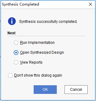
Figure 1.27 Synthesis Completed dialog box
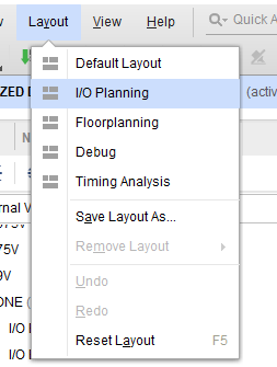
Figue 1.28 Excute I/O planning
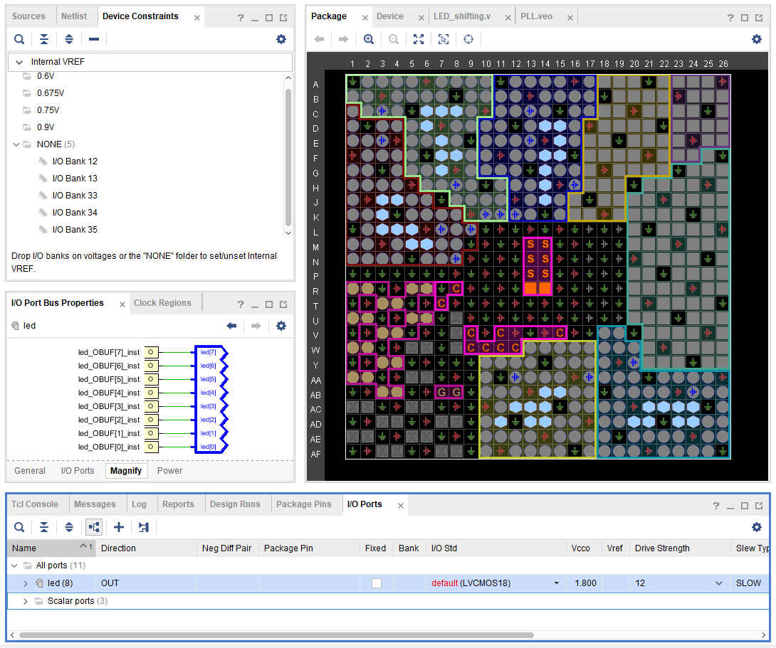
Figure 1.29 Pin assignment interface
- Pin assignment for each I / O, the pin mapping table is shown in Table 1.1, and the allocation result is shown in Figure 1.30.
Table 1.1 LED shifting experiment pin mapping table
| Signal Name | Network Name | FPGA Pin | Port Description |
| inclk_p | SYSCLK_P | AC13 | Input clock(differential)
200MHz |
| inclk_n | SYSCLK_N | AD13 | |
| rst | GPIO_SW_2 | F4 | External reset |
| led[0] | GPIO_DIP_SW0 | A17 | 8-bit LED |
| led[1] | GPIO_DIP_SW1 | E8 | |
| led[2] | GPIO_DIP_SW2 | C6 | |
| led[3] | GPIO_DIP_SW3 | B9 | |
| led[4] | GPIO_DIP_SW4 | B6 | |
| led[5] | GPIO_DIP_SW5 | H6 | |
| led[6] | GPIO_DIP_SW6 | H7 | |
| led[7] | GPIO_DIP_SW7 | G9 |
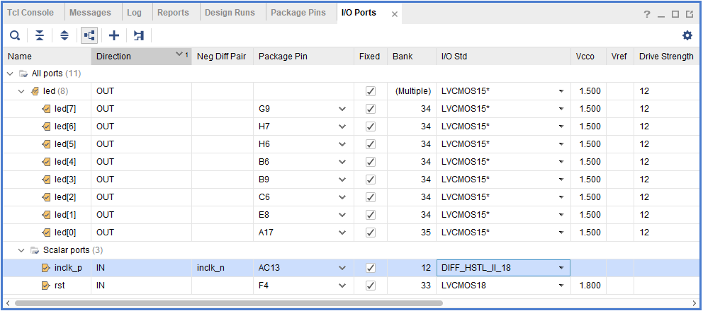
Figure 1.30 Pin assignment
The third step: implementation
After the pin assignment is completed, expand IMPLEMENTATION in the Flow Navigator window on the left side of the Vivado main interface, click Run Implementation, and the Save Constraints dialog box pops up, as shown in Figure 1.31.
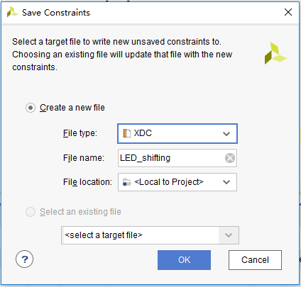
Figure 1.31 Save Constraints dialog box
The fourth step: generate programmable files
After completing the previous step, expand PROGRAM AND DEBUG in the Flow Navigator window on the left side of the main interface of Vivado. Click Generate Bitstream to generate a programmable bitstream file.
The fifth step: board verification
With the Zynq_7030 development board connected, expand the Open Hardware Manager, click Open Target, a floating command window appears, and choose to execute the Auto Connect command, as shown in Figure 1.32. Vivado will automatically search for the device, as shown in Figure 1.33. Successfully connected development board.
As shown in Figure 1.34, click Program device in the figure, the Program Device dialog box pops up, as shown in Figure 1.35. Select the correct bit stream (.bit) file, and click Program to download the file to FII-PRA100T development board.
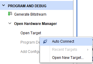
Figure 1.32 Execute Auto Connect command
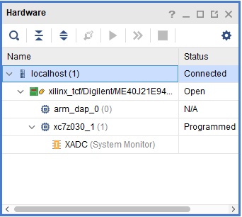
Figure 1.33 Successfully connected development board
![]()
Figure 1.34 Open program device
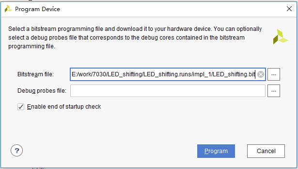
Figure 1.35 Program Device dialog box
The experimental phenomenon is shown in Figure 1.36.
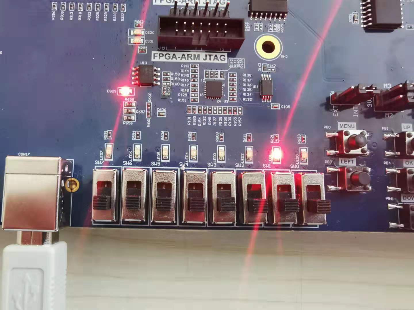
Figure 1.36 Experimental phenomenon of LED shifting
Experiment 2 Analysis of Switch Signals via ILA
2.1 Experiment Objective
- Continue to practice using develop board
- Continue to practice the call of system resource PLL
- Learn to use ILA (Integrated Logic Analyzer) in Vivado
2.2 Experiment Implement
Capture and analyze switch signals on the development board by using ILA
2.3 Experiment
2.3.1 Introduction of Switches
The on-board switch is 8 DIP switches, as shown in Figure 2.1. The switch is used to switch the circuit by turning the switch handle.
Figure 2.1 Switch physical picture
2.3.2 Hardware Design
The schematics of the switch is shown in Figure 2.2. One end of the 8-bit switch is connected to the VCC1V5_ALL terminal at the same time, which is at a high level. One end is respectively connected to an LED, and is connected to the control terminal SW_LED of the connected LED. When the DIP switch is selected, the FET is turned on at a high level, the LED is on, and a high-level signal is input to the FPGA at the same time. At this time, the LED will act as a switch strobe indication signal, and will light up when strobe.
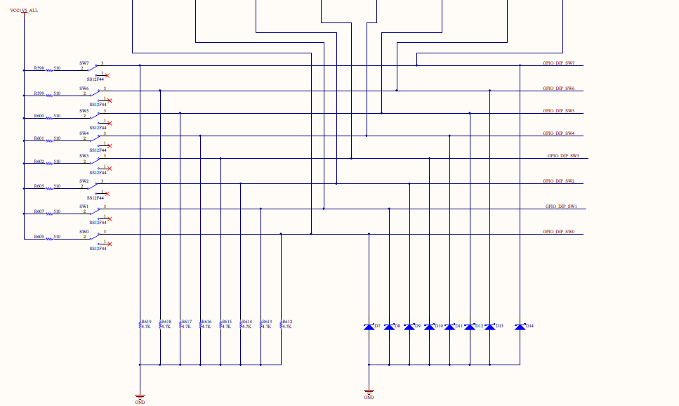
Figure 2.2 Schematics of the switches
2.3.3 Program Design
The first step: the establishment of the main program framework (interface design)
| module SW_LED(
input inclk_p, input inclk_n, input [7:0] sw, output reg [7:0] led );; endmodule |
The input signals for this experiment are differential clock signals inclk_p and inclk_n, 8-bit switch sw, and 8-bit led lights as output signals.
The second step: design content
| wire sys_clk;
wire pll_locked; reg sys_rst; clk_wiz_0 clk_wiz_0_inst( .clk_in1_p (inclk_p), .clk_in1_n (inclk_n), .reset (1’b0), .locked (pll_locked), .clk_out1 (sys_clk) ); always @ (posedge sys_clk) sys_rst <= !pll_locked; always @ (posedge sys_clk) begin if (sys_rst) led <= 8’d0; else led <= ~sw; end |
When the reset signal is valid, all 8 LEDs are off. After the reset is completed, the on/off of the LED is controlled by the switch, and the LED is on when the switch is on. (Due to hardware design reasons, LEDs are temporarily assigned to the segment display when constraints are added.)
2.4 Experiment Verification
(Refer to Experiment 1 for the board verification process in subsequent tests, which will not be described in detail)
The first step: add constraints and assign pins
The pin assignments are shown in Table 2.1.
Table 2-1 Switch and display experiment pin mapping table
| Signal Name | Network Name | FPGA Pin | Port Description |
| inclk_p | SYSCLK_P | AC13 | Input clock (differential)
200MHz |
| inclk_n | SYSCLK_N | AD13 | |
| sw[0] | GPIO_DIP_SW0 | A17 | 8-bit switch |
| sw[1] | GPIO_DIP_SW1 | E8 | |
| sw[2] | GPIO_DIP_SW2 | C6 | |
| sw[3] | GPIO_DIP_SW3 | B9 | |
| sw[4] | GPIO_DIP_SW4 | B6 | |
| sw[5] | GPIO_DIP_SW5 | H6 | |
| sw[6] | GPIO_DIP_SW6 | H7 | |
| sw[7] | GPIO_DIP_SW7 | G9 | |
| led[0] | SEF_PA | J10 | 8-bit LED
(segment display) |
| led[1] | SEF_PB | J9 | |
| led[2] | SEF_PC | A7 | |
| led[3] | SEF_PD | B7 | |
| led[4] | SEF_PE | A8 | |
| led[5] | SEF_PF | A9 | |
| led[6] | SEF_PG | A10 | |
| led[7] | SEF_DP | B10 |
The second step: run the implementation, generate bitstream files, and verify the board
After successfully downloading the generated programmable bitstream file to the Zynq_7030 development board, the experimental phenomenon is shown in Figure 2.3. Toggle the switch and the corresponding LED lights up.
2.5 Use of ILA
Design synthesis and adding constraints have been completed during the board verification. Therefore, expand the SYNTHESIS option under the Flow Nvigator window on the left side of the Vivado main interface, click Open Synthesized Design, and in the Sources window, click Netlist to open the netlist structure generated after the synthesis. All network nodes are under the Nets folder, as shown in Figure 2.4.
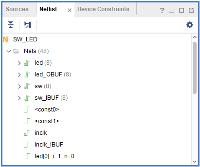
Figure 2.4 Netlist
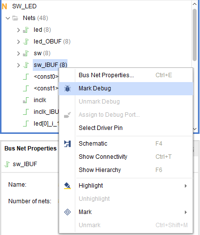
Figure 2.5 Mark network nodes to be debugged
As shown in Figure 2.5, right-click the network node to be debugged, and a floating command window appears. Click Mark Debug to mark the target network node. After all signals that need to be adjusted are marked (this experiment needs to debug the switch signal sw and the LED light signal led), click Tools on the Vivado menu bar, run the Set Up Debug command, and the Set Up Debug dialog box pops up, as shown in Figure 2.6.
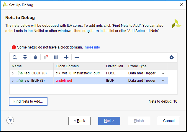
Figure 2.6 Set Up Debug dialog box
In Figure 2.6, all marked network nodes are in the window. Some signals need to manually add the clock domain. like sw_IBUF in this experiment. Clock Domain is displayed as red undefined. Right-click the network node without the clock, such as shown in Figure 2.7, the floating command dialog box pops up. Click the Select Clock Domain command to pop up the dialog box. As shown in Figure 2.8, select the 100MHz clock output by the PLL as the clock of the sw network node, and click the OK button. The clock is successfully added. Click the Next button in the Set Up Debug dialog box.
As shown in Figure 2.9, in the following settings, the Sample of data depth is set according to actual needs. For this experiment, the default value is 1024. For the input pipe stages, the default value is 0. Under the Trigger and Storage Settings option, check the Capture control and Advanced trigger options, click the Next button, and click the Finish button in the pop-up dialog box to complete the debugging settings.
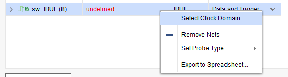
Figure 2.7 Adding a clock domain
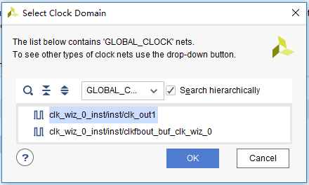
Figure 2.8 Selecting the clock
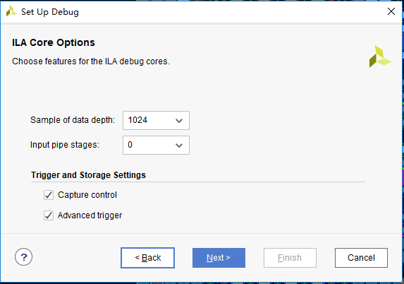
Figure 2.9 Other debugging settings
After completing the debugging and setting, refer to Experiment 1, re-run the design synthesis, run the implementation, and generate the bitstream file (the project without added constraints needs to add additional constraint files), and then program the board. After success, the Vivado interface will automatically jump to the debugging interface, as shown in Figure 2.10.
Expand led and sw. At this time, the 8-bit switches are all 0 and unselected. The LEDs are all 1 and off. As shown in Figure 2.11.
Set the trigger condition to sw! = 8’h00, and click to run ILA, as shown in Figure 2.12.
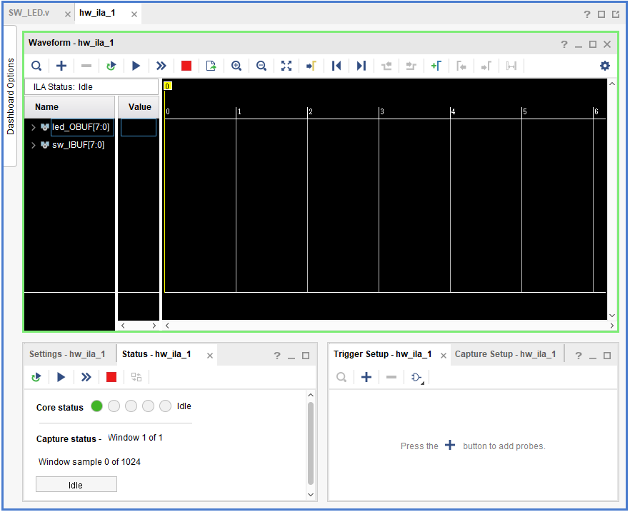
Figure 2.10 ILA debugging interface
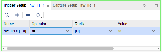
Figure 2.11 Set trigger conditions
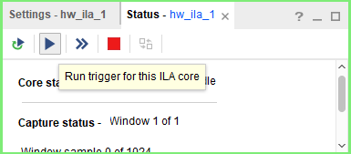
Figure 2.12 Running ILA
Pull up the first bit switch sw [1], as shown in Figure 2.13. At the position shown by the T red line, the left side is the previous state, and the right side is the post-trigger state. When the trigger condition is met, sw [1] changes from 0 to 1, switch 1 is on, and at the same time, led [1] changes from 1 to 0. The LED 1 is on, corresponding to the FII-PRA100T development board at this time, which is in line with the debugging results.
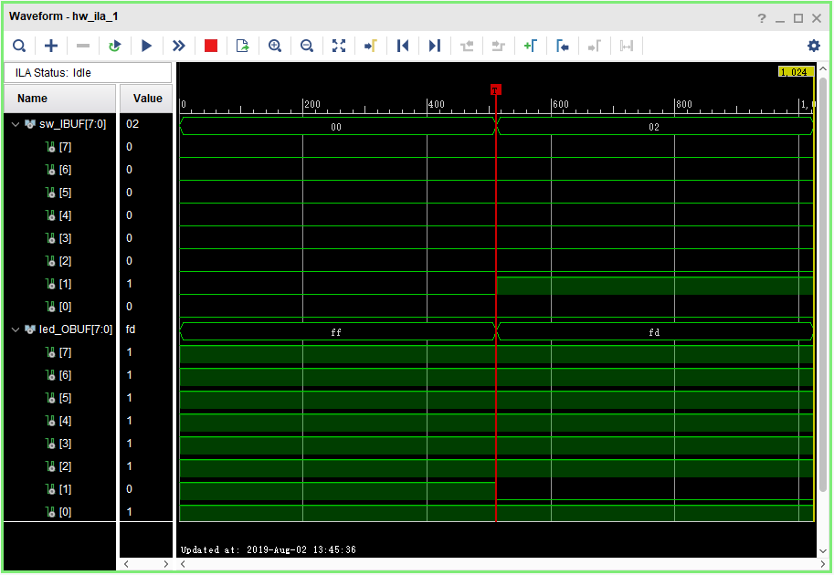
Figure 2.13 Debugging results
Set different trigger conditions, observe and analyze the experimental results.
Experiment 3 Segment Display Digital Clock Experiment
3.1 Experiment Objective
- Review the contents of experiment 1 and experiment 2, master the configuration of PLL, the design of frequency divider, the principle of schematics and the pin assignment of FPGA. Familiar with the design of Verilog’s tree hierarchy
- Study BCD decoder
- Display design of hexadecimal to 7 segment display decoders
- Achieve digital clock display
3.2 Experiment Implement
- The display decoder has two lower digits to display seconds, the middle two digits to display minutes, and the highest two digits to display hours.
- Separate the seconds, minutes, and hours with decimal points
3.3 Experiment
3.3.1 Introduction to Segment Display Decoder
One type of segment display is a semiconductor light-emitting device. The segment display can be divided into a seven-segment display decoder and an eight-segment display decoder. The difference is that the eight-segment display decoder has one more unit for displaying the decimal point, the basic unit is a light-emitting diode. The on-board segment display is a six-in-one eight-segment display decoder as shown in Figure 3.1, and its structure is shown in Figure 3.2.
Figure 3.1 Segment display decoder physcial picture
Figure 3.2 Segment decoder structure
Common anode decoders are used here. That is, the anodes of the LEDs are connected. See Figure 3.3. Therefore, the FPGA is required to control the cathode of the LED to be low level, illuminate the diode, and display the corresponding information. The six-digit common anode eight-segment display decoder refers to the signal that controls which one is lit, which is called the bit selection signal. The content displayed by each digital segment is called the segment selection signal. The corresponding truth table is shown in Table 3.1.
Figure 3.3 Schematics of common anode decoders
Table 3.1 8-segment display decoder truth table
| Signal Segment | DP | G | F | E | D | C | B | A |
| · | 0 | 1 | 1 | 1 | 1 | 1 | 1 | 1 |
| 0 | 1 | 1 | 0 | 0 | 0 | 0 | 0 | 0 |
| 1 | 1 | 1 | 1 | 1 | 1 | 0 | 0 | 1 |
| 2 | 1 | 0 | 1 | 0 | 0 | 1 | 0 | 0 |
| 3 | 1 | 0 | 1 | 1 | 0 | 0 | 0 | 0 |
| 4 | 1 | 0 | 0 | 1 | 1 | 0 | 0 | 1 |
| 5 | 1 | 0 | 0 | 1 | 0 | 0 | 1 | 0 |
| 6 | 1 | 0 | 0 | 0 | 0 | 0 | 1 | 0 |
| 7 | 1 | 1 | 1 | 1 | 1 | 0 | 0 | 0 |
| 8 | 1 | 0 | 0 | 0 | 0 | 0 | 0 | 0 |
| 9 | 1 | 0 | 0 | 1 | 0 | 0 | 0 | 0 |
| A | 1 | 0 | 0 | 0 | 1 | 0 | 0 | 0 |
| B | 1 | 0 | 0 | 0 | 0 | 0 | 1 | 1 |
| C | 1 | 1 | 0 | 0 | 0 | 1 | 1 | 0 |
| D | 1 | 0 | 1 | 0 | 0 | 0 | 0 | 1 |
| E | 1 | 0 | 0 | 0 | 0 | 1 | 1 | 0 |
| F | 1 | 0 | 0 | 0 | 1 | 1 | 1 | 0 |
There are two ways to display the decoders, static display and dynamic display.
Static display: each display segment is connected with an 8-bit data line to control and maintain the displayed glyph until the next segment selection signal arrives. The advantage is that the driver is simple, and the disadvantage is that it takes up too much I/O resources.
Dynamic display: parallel the segment selection lines of all display decoders, and the digit selection line controls which digit is valid and lights up. Through the afterglow effect of the LED and the persistence effect of the human eye, the display decoder appears to be continuously lit at a certain frequency. The advantage is to save I / O resources, the disadvantage is that the driver is more complicated, the brightness is not high as static display.
In this experiment, the segment display was driven by dynamic scanning.
3.3.2 Hardware Design
The schematics of the segment display is shown in Figure 3.4. The anode is connected to VCC through the P-channel field corresponding tube. Therefore, when the bit selection signal SEG_3V3_D[0:5] is low level 0, the FET is turned on, the anode of the display decoder is high level; the cathode (segment selection signal) SEG_PA, SEG_PB, SEG_PC, SEG_PD, SEG_PE, SEG_PF, SEG_PG, SEG_DPZ are directly connected to the FPGA and directly controlled by the FPGA. Therefore, when the bit selection signal is 0, and the segment selection signal is also 0, the segment display is lit.
Figure 3.4 Schematics of the segment display
3.3.3 Program Design
The first step: the establishment of the main program framework (interface design)
| module BCD_counter(
input inclk_p, input inclk_n, input rst, output reg [7:0] tube_seg, output reg [5:0] tube_sel ); endmodule |
The input signal has a clock and a reset signal, and the output signal is a segment selection signal seven_seg and a new signal scan.
Refer to Experiment 1 for the control module, frequency division module and counting module.
The second step: system control module
| module sys_control(
input inclk_p, input inclk_n, input rst, output sys_clk, output reg sys_rst, output reg ext_rst ); wire pll_locked; //PLL instantiation clk_wiz_0 clk_wiz_0_inst( .clk_in1_p (inclk_p), .clk_in1_n (inclk_n), .reset (1’b0), .locked (pll_locked), .clk_out1 (sys_clk) ); //reset signal always @ (posedge sys_clk) begin sys_rst <= !pll_locked; ext_rst <= rst; end endmodule |
In the first sub-module (system control module), the input clock is the system 200 MHz differential clock, and a 100MHz is output through the PLL as the working clock of the other sub-modules. At the same time, the PLL lock signal pll_locked is inverted as the system reset signal, and the key reset rst is registered as the external hardware reset signal est_rst.
The third step: frequency division
With reference to Experiment 1, a millisecond pulse signal and a second pulse signal are output as input signals of the segment display driving module.
The fourth step: segment display driving module
- Counting section
The counting part is similar to the frequency dividing module. It is timed by the second pulse signal for 60 seconds, 60 minutes, 24 hours, and when the time reaches 23 hours, 59 minutes and 59 seconds, the counters are all cleared, which is equivalent to one day.
- Segment display dynamic scanning part
| // Segment display dynamic scanning, implemented by the state machine
reg count_seg; reg point; reg scan_state reg [3:0] counta,countb; //second counter reg [3:0] countc,countd; //minute counter reg [3:0] counte,countf; //hour counter always @ (posedge clk) begin if(rst) begin tube_sel <= 6’b111_111; count_seg <= 4’d0; point <= 1’b1; scan_state <= 0; end else case (scan_state) 0 : begin tube_sel <= 6’b111_110; count_seg <= counta; point <= 1’b1; if (ms_f) scan_state <= 1; end
1 : begin tube_sel <= 6’b111_101; count_seg <= countb; point <= 1’b1; if (ms_f) scan_state <= 2; end
2 : begin tube_sel <= 6’b111_011; count_seg <= countc; point <= 1’b0; if (ms_f) scan_state <= 3; end
3 : begin tube_sel <= 6’b110_111; count_seg <= countd; point <= 1’b1; if (ms_f) scan_state <= 4; end
4 : begin tube_sel <= 6’b101_111; count_seg <= counte; point <= 1’b0; if (ms_f) scan_state <= 5; end
5 : begin tube_sel <= 6’b011_111; count_seg <= countf; point <= 1’b1; if (ms_f) scan_state <= 0; end
default : scan_state <= 0; endcase end |
The dynamic scanning of the segment display is realized by the state machine. A total of six segment display require six states. The state machine scan_state[2:0] is defined, and the corresponding content count_sel is displayed in different states. At reset, all six segment display are extinguished and jump to the 0 state. The segment display is dynamically scanned in 1 millisecond time driven by a millisecond pulse:
In the 0 state, the 0th segment display is lit, and the ones digit of the second is displayed;
In the 1 state, the first segmentdisplay is lit, and the tens digit of the second is displayed;
In the 2 state, the second segment display is lit, and the ones digit of the minute is displayed, the decimal point lights up, distinguishing between seconds and minutes;
In the 3 state, the third segment display is lit, and the tens digit of the minute is displayed;
In the 4 state, the fourth segment display is lit, and the ones digit of the hour is displayed, the decimal point lights up, distinguishing between minutes and hours;
In the 5 state, the fifth segment display is lit, and the tens digit of the hour is displayed;
The third step: segment code display section
| always @ (posedge sys_clk)
begin if (ext_rst) tube_seg <= 8’d0; else case (counta) 0 : tube_seg <= 8’b0100_0000; 1 : tube_seg <= 8’b0111_1001; 2 : tube_seg <= 8’b0010_0100; 3 : tube_seg <= 8’b0011_0000; 4 : tube_seg <= 8’b0001_1001; 5 : tube_seg <= 8’b0001_0010; 6 : tube_seg <= 8’b0000_0010; 7 : tube_seg <= 8’b0111_1000; 8 : tube_seg <= 8’b0000_0000; 9 : tube_seg <= 8’b0001_0000; default : tube_seg <= 8’b0100_0000; endcase end // Set decimal points between seconds, minites, and hours always @ (posedge clk) tube_seg <= {point, seven_seg_r}; |
Referring to Table 3.1, the characters to be displayed are corresponding to the segment code, and the decimal point is composed of the final segment selection signal tube_seg in the form of bit splicing.
3.4 Experiment Verification
The first step: add contraints and assign pins
The pin assignments are shown in Table 3.2.
Table 3.2 Segment display experimental pin mapping table
| Signal Name | Network Name | FPGA Pin | Port Description |
| inclk_p | SYSCLK_P | AC13 | Input Clocl (differential)
200MHz |
| inclk_n | SYSCLK_N | AD13 | |
| rst | GPIO_SW_2 | F4 | reset |
| scan[0] | SEG_D0 | C1 | Bit Selection Signal |
| scan[1] | SEG_D1 | E3 | |
| scan[2] | SEG_D2 | F7 | |
| scan[3] | SEG_D3 | D6 | |
| scan[4] | SEG_D4 | H11 | |
| scan[5] | SEG_D5 | J11 | |
| seven_seg[0] | SEF_PA | J10 | Segment Selection Signal |
| seven_seg[1] | SEF_PB | J9 | |
| seven_seg[2] | SEF_PC | A7 | |
| seven_seg[3] | SEF_PD | B7 | |
| seven_seg[4] | SEF_PE | A8 | |
| seven_seg[5] | SEF_PF | A9 | |
| seven_seg[6] | SEF_PG | A10 | |
| seven_seg[7] | SEF_DP | B10 |
The second step: run the implementation, generate bitstream files, and verify the board
After successfully downloading the generated programmable bitstream file to the Zynq_7030 development board, the experimental phenomenon is shown in Figure 3.5.

Figure 2.3 Segment display experimental phenomenon
Experiment 4 Button Debounce
4.1 Experiment Objective
- Review the design process of the shifting LED
- Learn button debounce principle and adaptive programming
- Learn the connection and use of the Zynq_7030 button hardware circuit
- Comprehensive application button debounce and other conforming programming
4.2 Experiment Implement
- Control the movement of the lit LED by pressing the button
- Each time the button is pressed, the lit LED moves one bit.
- When the left shift button is pressed, the LED moves to the left, presses the right button, and the LED moves to the right.
4.3 Experiment
4.3.1 Introduction to Button and Debounce Principle
- Introduction to button
The on-board button is a common push button, which is valid when pressed, and automatically pops up when released. A total of eight, respectively, PB1 (MENU), PB2 (UP), PB3 (RETURN), PB4 (LETF), PB5 (OK), PB6 (RIGHT), PB7 (DOWN) and a hardware reset button (RESET). As shown in Figure 4.1.
Figure 4.1 Button physical picture
Introduction to button debounce
As long as mechanical buttons are used, instability should be considered. Usually, the switches used for the buttons are mechanical elastic switches. When the mechanical contacts are opened and closed, due to the elastic action of the mechanical contacts, a push button switch does not immediately turn on when closed, nor is it off when disconnected. Instead, there is some bouncing when connecting and disconnecting. See Figure 4.2.
The length of the button’s stable closing time is determined by the operator. It usually takes more than 100ms. If you press it quickly, it will reach 40-50ms. It is difficult to make it even shorter. The bouncing time is determined by the mechanical characteristics of the button. It is usually between a few milliseconds and tens of milliseconds. To ensure that the program responds to the button’s every on and off, it must be debounced. When the change of the button state is detected, it should not be immediately responding to the action, but waiting for the closure or the disconnection to be stabilized before processing. Button debounce can be divided into hardware debounce and software debounce.
Figure 4. 2 Button bounce principle
In most of cases, we use software or programs to achieve debounce. The simplest debounce principle is to wait for a delay time of about 10ms after detecting the change of the button state, and then perform the button state detection again after the bounce disappears. If the state is the same as the previous state just detected, the button can be confirmed. The action has been stabilized. This type of detection is widely used in traditional software design. However, as the number of button usage increases, or the buttons of different qualities will react differently. If the delay is too short, the bounce cannot be filtered out. When the delay is too long, it affects the sensitivity of the button.
4.3.2 Hardware Design
The schematics (part) of the button is shown in Figure 4.3. You can see that one side of the button (P1, P2) is connected to VCC, and the other side (P3, P4) is connected to the FPGA. At the same time, it is grounded through a 5.11K resistor. In the normal state, the button is left floating. At this time, the potential at button P3 is 0, so the input value to the FPGA is 0. When the button is pressed, both sides of the button are turned on. At this time, the potential at button P3 is VCC3.3V, so the button inputs a value of 1 into the FPGA. So the on-board push button is high effective.
Figure 4.3 Schematics of the push buttons
4.3.3 Program Design
Refer to the previous experiments for the frequency division module and new push buttons debounce module is introduced below.
Figure 4.4 Button deboucne flow chart
This chapter introduces an adaptive button debounce method: starts timing when a change in the state of the button is detected. If the state changes within 10ms, the button bouncing exists. It returns to the initial state, clears the delay counter, and re-detects the button state until the delay counter counts to 10ms. The same debounce method is used for pressing and releasing the button. The flow chart is shown in Figure 4. 4.Case 0 and 1 debounce the button press state. Case 2 and 3 debounce the button release state. After finishing the whole debounce procedure, the program outputs a synchronized clock pulse.
| module pb_ve (
input sys_clk, input sys_rst, input ms_f, input keyin, output keyout ); reg keyin_r; reg keyout_r; reg [1:0] ve_key_st; reg [3:0] ve_key_count; always @ (posedge sys_clk) begin keyin_r <= keyin; end always @ (posedge sys_clk) begin if (sys_rst) begin keyout_r <= 1’b0; ve_key_count <= 0; ve_key_st <= 0; end else case (ve_key_st) 0 : begin keyout_r <= 1’b0; ve_key_count <= 0; if (keyin_r) ve_key_st <= 1; end 1 : begin if (!keyin_r) ve_key_st <= 0; else begin if (ve_key_count == 10) ve_key_st <= 2; else if (ms_f) ve_key_count <= ve_key_count + 1’b1; end end 2 : begin ve_key_count <= 0; if (!keyin_r) ve_key_st <= 3; end 3 : begin if (keyin_r) ve_key_st <= 2; else begin if (ve_key_count == 10) begin ve_key_st <= 0; keyout_r <= 1’b1; end else if (ms_f) ve_key_count <= ve_key_count + 1’b1; end end default : ; endcase end assign keyout = keyout_r; endmodule |
Button-controlled LED display module
| module led_shift(
input sys_clk, input rst, input key_left, input key_right, input s_f, output reg [7:0] led ); always @ (posedge sys_clk) begin if (rst) led <= 8’hff; else begin if (key_left) begin if (led == 8’hff) led <= 8’b0000_0001; else led <= {led[6:0], led[7]}; end else if (key_right) begin if (led == 8’hff) led <= 8’b1000_0000; else led <= {led[0], led[7:1]}; end end end endmodule |
In the reset state, all the 8-bit LED is on. When the button is pressed, only one LED is on. After that, each time the push button is pressed, the LED moves according to the corresponding signal.
4.4 Experiment Verification
The first step: add constraints and assign the pins
The pin assignment is shown in Table 4.1.
Table 4.1 Button debounce experiment pin mapping table
| Signal Name | Network Name | FPGA Pin | Port Description |
| inclk_p | SYSCLK_P | AC13 | Input clock (Differential)
200MHz |
| inclk_n | SYSCLK_N | AD13 | |
| rst | GPIO_SW_2 | F4 | External reset |
| left | GPIO_SW_3 | D4 | Left shift signal |
| right | GPIO_SW_5 | F2 | Right shift signal |
| led[0] | GPIO_DIP_SW0 | A17 | 8-bit LED |
| led[1] | GPIO_DIP_SW1 | E8 | |
| led[2] | GPIO_DIP_SW2 | C6 | |
| led[3] | GPIO_DIP_SW3 | B9 | |
| led[4] | GPIO_DIP_SW4 | B6 | |
| led[5] | GPIO_DIP_SW5 | H6 | |
| led[6] | GPIO_DIP_SW6 | H7 | |
| led[7] | GPIO_DIP_SW7 | G9 |
The second step: run the implementation, generate bitstream files, and verify the board
After successfully downloading the generated programmable bitstream file to the Zynq_7030 development board, the experimental phenomena are shown in Figures 4.5 to 4.7.
Figure 4.5 Experiment Result(reset)
When the right shift button is pressed, the highest LED lights up. See Figure 4.6.
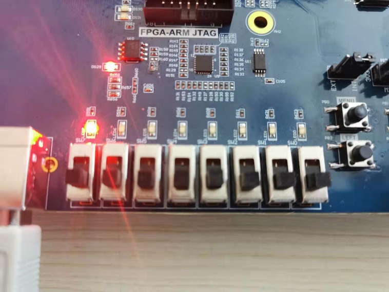
Figure 4.6 Experiment result(one right shift)
Press the right shift button again and the LED will move one bit to the right. See Figure 4.7.
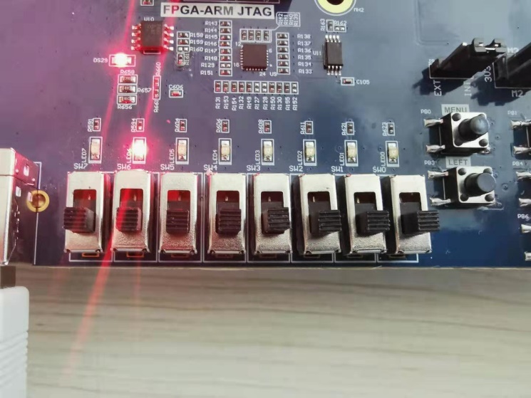
Figure 4.7 Experiment result(another right shift)
Experiment 5 Digital Clock Comprehensive Experiment
5.1 Experiment Objective
- Review the segment display content of experiment 3, and the button debounce content of experiment 4;
- Combine experiment 3 and experiment 4 to design a complete adjustable digital clock;
5.2 Experiment Implement
- Set four push buttons (left, right, up, down);
- Left and right push buttons control the calibration function, switch between segment display of hour, minute and second;
- Up and down calibration by adding 1 and subtracting 1 to the data to be calibrated;
- Modular design so that the design can be reused
- Learn to use module parameters
- Learn to use Vivado’s timing analysis function and be able to constrain the clock signal correctly
5.3 Experiment
5.3.1 Hardware Design
Refer to experiment 3 and experiment 4 for hardware design.
5.3.2 Program Design
The first step: the establishment of the main program framework (interface design)
| module adj_clock(
input inclk_p, input inclk_n, input [6:0] PB,
output [5:0] tube_sel, output [6:0] tube_seg, output point ); endmodule |
Because many push buttons are used, the 7-digit push buttons are defined in the form of PB [6: 0] bus. During the calibration time, the decimal point functions as a flag bit, which can be moved under the key drive and output separately.
The second step: system control module
Refer experiment 3.
The third step: frequency division
Refer experiment 1.
The fourth step: button debounce module
Refer experiment 4.
The fifth step: adjustable digital clock module
| always @ (posedge clk)
begin if (!rst) point_r <= 8’b1111_1110; else begin if (PB_flag[3]) point_r <= {point_r[6:0], point_r[7]}; else if (PB_flag[5]) point_r <= {point_r[0], point_r[7:1]}; end end |
For decimal point, when the reset is valid, it lights up at the lowest position. When the left shift key PB_flag [3] is valid, the decimal point is shifted one digit to the left, and when the right shift key PB_flag [5] is valid, the decimal point is shifted one digit to the right.
| //Second (top level instantiation)
dual_num_count #(.PAR_COUNTA(9), //Paramters passing .PAR_COUNTB(5) ) dual_num_count_sec ( .clk (clk), .rst (rst), .adj_add (PB_flag[1]), .adj_sub (PB_flag[6]), .adj_point (point_r[1:0]), .i_trig_f (s_f), .o_trig_f (min_f), .counta (count_secl), .countb (count_sech) ); //Calibration module module dual_num_count #(parameter PAR_COUNTA=9, parameter PAR_COUNTB=5 ) ( input clk, input rst, input adj_add, input adj_sub, input [1:0] adj_point, input i_trig_f, output reg o_trig_f, output reg [3:0] counta, output reg [3:0] countb ); always @ (posedge clk) begin if (!rst) begin counta <= 0; countb <= 0; o_trig_f <= 1’b0; end else begin o_trig_f <= 1’b0; if (adj_add) begin if (!adj_point[0]) begin if (counta == 9) counta <= 0; else counta <= counta + 1’b1; end else if(!adj_point[1]) begin if (countb == 9) countb <= 0; else countb <= countb + 1’b1; end end
else if (adj_sub) begin if (!adj_point[0]) begin if (counta == 0) counta <= 4’d9; else counta <= counta – 1’b1; end else if (!adj_point[1]) begin if (countb == 0) countb <= 4’d9; else countb <= countb – 1’b1; end end
else if (i_trig_f) begin o_trig_f <= 1’b0; if ((countb == PAR_COUNTB) && (counta == PAR_COUNTA)) begin counta <= 4’d0; countb <= 4’d0; o_trig_f <= 1’b1; end else begin if (counta == PAR_COUNTA) begin counta <= 4’d0; if (countb == PAR_COUNTB) countb <= 4’d0; else countb <= countb + 1’b1; end else counta <= counta + 1’b1; end end end end endmodule |
In the calibration part, a general module is instantiated four times, and the data of seconds, minutes, hours, and days are calibrated respectively. At the same time, the values of different internal variables are assigned in the form of parameter passing.
Take the second part as an example, enter the decimal point point [1: 0], that is, the 0th and first digits of the segment display, to illustrate the second. When the reset is valid, the counter counta = 0, countb = 0, and the output pulse (second module output pulse is the minute pulse min_f) o_trig_f = 1’b0; when the calibration signal (adj_add is a plus 1 signal and adj_sub is a minus 1 signal) is valid, the corresponding one with the decimal point lit is calibrated accordingly. Otherwise, driven by the input pulse (the input pulse of the second module is the second pulse s_f), counta increases from 0 to the parameter PAR_COUNTA (9), and countb increases from 0 to the parameter PAR_COUNTB (5). When counta = PAR_COUNTA and countb = PAR_COUNTB, both counters are cleared and the output pulse o_trig_f = 1’b1. The two counters count a total of 60, so one pulse is output in one minute.
5.4 Experiment Verification
The first step: add constraints and assign the pins
See Table 5.1 for the pin assignment.
Table 5.1 Digital clock experiment pin mapping table
| Signal Name | Network Name | FPGA Pin | Port Description |
| inclk_p | SYSCLK_P | AC13 | Input clock (differential)
200MHz |
| inclk_n | SYSCLK_N | AD13 | |
| PB[0] | GPIO_SW_0 | L9 | 7-bit push button |
| PB[1] | GPIO_SW_1 | G4 | |
| PB[2] | GPIO_SW_2 | F4 | |
| PB[3] | GPIO_SW_3 | D4 | |
| PB[4] | GPIO_SW_4 | D3 | |
| PB[5] | GPIO_SW_5 | F2 | |
| PB[6] | GPIO_SW_6 | G2 | |
| tube_sel[0] | SEG_D0 | C1 | Bit selection signal |
| tube_sel[1] | SEG_D1 | E3 | |
| tube_sel[2] | SEG_D2 | F7 | |
| tube_sel[3] | SEG_D3 | D6 | |
| tube_sel[4] | SEG_D4 | H11 | |
| tube_sel[5] | SEG_D5 | J11 | |
| tube_seg[0] | SEF_PA | J10 | Segement selection signal |
| tube_seg[1] | SEF_PB | J9 | |
| tube_seg[2] | SEF_PC | A7 | |
| tube_seg[3] | SEF_PD | B7 | |
| tube_seg[4] | SEF_PE | A8 | |
| tube_seg [5] | SEF_PF | A9 | |
| tube _seg[6] | SEF_PG | A10 | |
| tube _seg[7] | SEF_DP | B10 |
The second step: run the implementation, generate bitstream files, and verify the board
After successfully downloading the generated programmable bitstream file to the Zynq_7030 development board, the experimental phenomenon is shown in Figure 5.1.
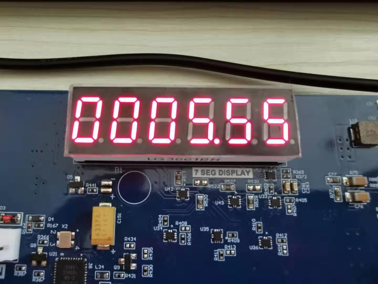
Figure 5.1 Digital clocl comprehensive design result
Experiment 6 Use of Multipliers and ISIM
6.1 Experiment Objective
- Learn to use multiplier
- Use ISIM to simulate design output
6.2 Experiment Implement
- 8×8 multiplier, the first input value is an 8-bit switch, and the second input value is the output of an 8-bit counter.
- Observe the output in ISIM
6.3 Experiment
6.3.1 Program Design
The first step: the establishment of the main program framework
| module mult_sim(
input inclk_p, input inclk_n, input [7:0] sw, output [15:0] mult_res, output reg [7:0] count ); endmodule |
The second step: call multiplier IP core
Refer to experiment 1. Call the multiplier IP core in the IP core directory, as shown in Figure 6.1. Enter mult in the search field to find Multiplier.
Double-click to select the multiplier configuration interface shown in Figure 6.2. Configure the multiplier IP core according to the parameters in the figure.
In the Basic window:
- Component Name: mult_8x8
- Data Type: Signed
- Width: 8
Under the Output and Control window, as shown in Figure 6.3:
Pipeline:1
Others are set by default.
Click OK and follow the steps to generate the multiplier IP core.
Figure 6.1 Search multiplier IP core
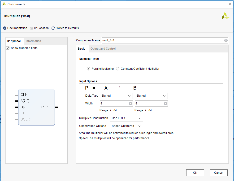
Figure 6.2 Multiplier input parameter settings
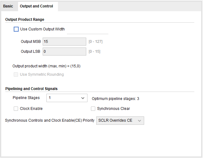
Figure 6.3 Multiplier output settings
The third step: instantiate the multiplier into the design file
| wire pll_locked;
wire sys_clk; reg sys_rst; mult_8x8 mult_8x8_inst( .CLK (sys_clk), .A (sw), .B (count), .P (mult_res) ) always @ (posedge sys_clk) sys_rst <= !pll_locked; always @ (posedge sys_clk) begin if (sys_rst) count <= 8’d0; else count <= count +1’b1; end |
6.4 Compile and Call of ISIM Simulation and Modelsim Simulation Library
Under the Vivado platform, you can choose to use built-in simulation tool ISIM or third-party simulation tools for functional simulation of the project. Simulating with the Modelsim simulation tool requires a separate compilation of the simulation library. This experimentd uses the built-in ISIM tool emulation and briefly introduce Modelsim’s Xilinx simulation library file compilation for simulation using Modelsim.
The first step: build simulation project files
Add simulation source files in the Sources window of the main interface of Vivado, click Desgin Sources, select the Add Sources command in the pop-up floating window, select the Add or create simulation sources check box in the pop-up dialog box, create a new source file, refer to experiment 1, the file is named mult_sim_tb, as shown in Figure 6.4.
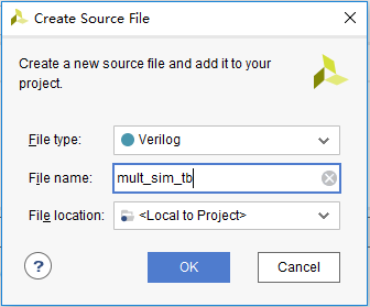
Figure 6.4 New simulation testbench file
After the creation is successful, the created testbench file will be automatically added in the sim_1 folder under the Sources window, as shown in Figure 6.5. Double-click to enter the design interface for design.

Figure 6.5 Create a simulation file.
The simulation file is as follows:
| module mult_sim_tb;
// Define the simulation signals reg inclk_p; reg inclk_n; reg rst; reg [7:0] sw; wire [15:0] mult_res; wire [7: 0] count; // Instantiate the simulation module mult_sim mult_sim_inst( .inclk_p (inclk_p), .inclk_n (inclk_n), .rst (rst), .sw (sw), .mult_res (mult_res), .count (count) ); // Initialize the simulation signals initial begin rst = 0; inclk_p = 1; sw = 0; #5 rst = 1; #15 sw = 20; #20 sw = 50;+ #20 sw = 100; #20 sw = 101; #20 sw = 102; #20 sw = 103; #20 sw = 104; #50 sw = 105; $monitor(“%d * %d=%d”, count, sw, mult_res); #1000000 $stop; end always begin #5 inclk_p=~inclk_p; inclk_n = !inclk_p; end endmodule |
The second step: run simulation
After saving the source file, find and expand the SIMULATION option under the Flow Navigator window on the main interface of Vivado, click Run Simulation, and click the Run Behavioral Simulation command in the pop-up floating window to start the ISIM simulation. The simulation interface is shown in Figure 6.6, the operation result mult_res appears one clock cycle later than the counter count.
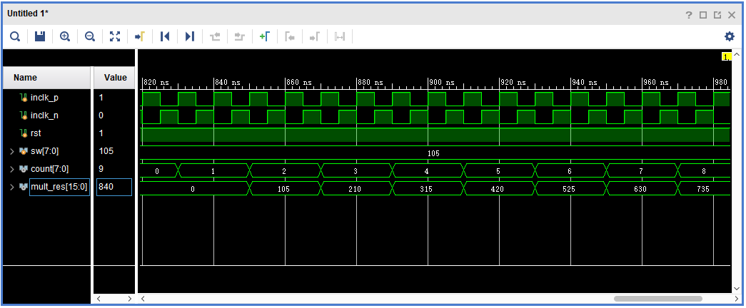
Figure 6.6 Simulation interface
Modelsim simulation library compilation:
When using Modelsim simulation, after installing Modelsim, the Xilinx simulation library file needs to be compiled first. The specific procedure is as follows
- Select compile simulation libraries under Tools in the menu bar, the following interface pops up shown in Figure 6.7.
- Set a full English path in the blue square in Figure 6.7. This path is to store the Modelsim and vivado joint simulation library files to be compiled and generated.
- Set as shown in the red sqaure in Figure 6.7, and select Modelsie (modelsim refers to the modelsim_se version. This version is a non-OEM version of the simulation tool launched by Mentor. Compared with the OEM version, it has a faster simulation speed and the number of simulation code lines are unlimited.) win64 under the installation path (select the win32 folder to install the x86 format Modelsie software). The joint simulation library of modelsim and vivado can be built. Click compile to start compiling the simulation library. The compiled library file is stored in the path set by the blue square in Figure 6.7.
- As shown in Figure 6. 8, the compilation is completed. Note that the process is very time consuming.
- More to practice
- Design an 8-bit trigger, simulate with ISIM
- Learn to write testbenches for simulation
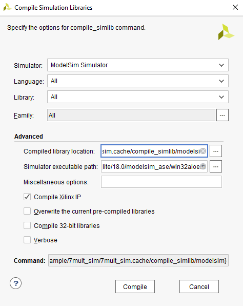
Figure 6.7 Compile library address settings
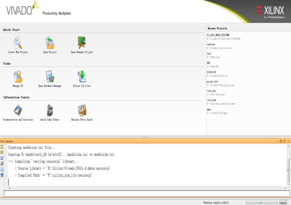
Figure 6.8 Successfully compiled the simulation library
Experiment 7 Hexadecimal Number to BCD Code Conversion and Application
Experiment Objective
- Learn to convert binary numbers to BCD (bin_to_bcd)
- Learn to convert hexadecimal numbers to BCD (hex_to_bcd)
7.2 Experiment Implement
Combined with experiment 6, display the calculation results on the segment display.
7.3 Experiment
7.2.1 Introduction to Hexadecimal Number to BCD Code Conversion
Since the hexadecimal display is not intuitive, decimal display is more widely used in real life.
Human eye recognition is relatively slow, so the display from hexadecimal to decimal does not need to be too fast. Generally, there are two methods
- Countdown method:
Under the control of the synchronous clock, the hexadecimal number is decremented by 1 until it is reduced to 0. At the same time, the appropriate BCD code decimal counter is designed to increment. When the hexadecimal number is reduced to 0, the BCD counter just gets with the same value to display.
- Bitwise operations (specifically, shift bits and plus 3 here). The implementation is as follows:
- Set the maximum decimal value of the expression. Suppose you want to convert the 16-digit binary value (4-digit hexadecimal) to decimal. The maximum value can be expressed as 65535. First define five four-digit binary units: ten thousand, thousand, hundred, ten, and one to accommodate calculation results
- Shift the hexadecimal number by one to the left, and put the removed part into the defined variable, and judge whether the units of ten thousand, thousand, hundred, ten, and one are greater than or equal to 5, and if so, add the corresponding bit to 3 until the 16-bit shift is completed, and the corresponding result is obtained.
Note: Do not add 3 when moving to the last digit, put the operation result directly
- The Principle of hexadecimal number to BCD number conversion
Suppose ABCD is a 4-digit binary number (possibly ones, 10 or 100 bits, etc.), adjusts it to BCD code. Since the entire calculation is implemented in successive shifts, ABCDE is obtained after shifting one bit (E is from low displacement and its value is either 0 or 1). At this time, it should be judged whether the value is greater than or equal to 10. If so, the value is increased by 6 to adjust it to within 10, and the carry is shifted to the upper 4-bit BCD code. Here, the pre-movement adjustment is used to first determine whether ABCD is greater than or equal to 5 (half of 10), and if it is greater than 5, add 3 (half of 6) and then shift.
For example, ABCD = 0110 (decimal 6)
- After shifting it becomes 1100 (12), greater than 1001 (decimal 9)
- By plus 0110 (decimal 6), ABCD = 0010, carry position is 1, the result is expressed as decimal
- Use pre-shift processing, ABCD = 0110 (6), greater than 5, plus 3
- ABCD=1001(9), shift left by one
- ABCD=0010, the shifted shift is the lowest bit of the high four-bit BCD.
- Since the shifted bit is 1, ABCD = 0010(2), the result is also 12 in decimal
- The two results are the same
- Firstly, make a judgement, and then add 3 and shift. If there are multiple BCD codes at the same time, then multiple BCD numbers all must first determine whether need to add 2 and then shift.
- The first way is relatively easy. Here, the second method is mainly introduced.
Example 1: bin_to_bcd

Figure 7.1 Example 1, bin_to_bcd
Example 2: Hex to BCD, the process is shown in Figure 7.2.
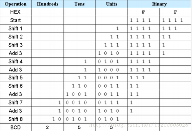
Figure 7.2 hex_to_bcd
7.2.2 Program Introduction
The first step: the establishment of the main program framework (interface design)
| module HEX_BCD (
input [15:0] hex, output reg [3:0] ones, output reg [3:0] tens, output reg [3:0] hundreds, output reg [3:0] thousands, output reg [3:0] ten_thousands ); |
Enter a 16-bit binary number hex, which can represent up to 65535 in decimal, so output one-digit ones, ten-digit tens, hundred-digit hundreds, thousands digit thousands, and ten-thousand digit ten_thousands.
The second step: implementation of fast algorithm
| reg [15:0] hex_reg;
integer i; always @ (*) begin hex_reg = hex; ones = 0; tens = 0; hundreds = 0; thousands = 0; ten_thousands = 0;
for (i = 15; i >= 0; i = i-1) begin if(ten_thousands >= 5) ten_thousands = ten_thousands + 3; if(thousands >= 5) thousands = thousands + 3; if(hundreds >= 5) hundreds = hundreds + 3; if(tens >= 5) tens = tens + 3; if(ones >= 5) ones = ones + 3; ten_thousands = ten_thousands << 1; ten_thousands[0] = thousands[3]; thousands = thousands << 1; thousands[0] = hundreds[3]; hundreds = hundreds << 1; hundreds[0] = tens[3]; tens = tens << 1; tens[0]= ones[3]; ones = ones << 1; ones[0] = hex_reg[15]; hex_reg = {hex_reg[14:0], 1’b0}; end end |
Referring to Figure 7.2, the first part of the program is the judgment and calculation part, if it is larger or equal to 5, add 3, and the latter part is the shift part.
The third step: verification
Refer to experiment 6, and use Modelsim for simulation. The simulation conditions are set as follows:
| initial begin
hex = 0 ; repeat (20) begin #10; hex = {$random}%20000; #10; end end |
At the beginning, the 16-bit binary number is equal to 0, and then it is delayed by 10ns. The 16-bit binary number is taken as a random number less than 20,000. The delay is ended after 10ns, and the entire process is repeated 20 times.
Refer to experiment 6. After running the simulation, the simulation results are shown in Figure 7.3.
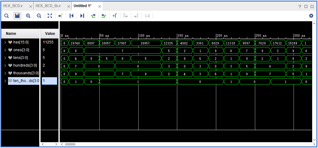
Figure 7.3 Simulation result
Application of Hexadecimal Number to BCD Code Conversion
Continue to complete the multiplier of experiment 6 and display the result in a segment display in decimal. Every 1s clock passes, the calculation result on the segment display changes once. The experiment requires frequency division, segment display, multiplier, and Hex to BCD conversion code. Refer to the previous experiments, and instantiate the parts in the new top level entity.
After completing the implementation, find and expand the IMPLEMENTATION option under the Flow Navigator window on the main interface of Vivado, expand Run Implementated Design, and click Report Timing Summary to view the circuit timing report. As shown in Figure 7.4, the timing requirements are satisfied.
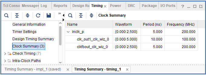
Figure 7.4 Timing report
7.5 Experiment Verification
The first step: add cosntraints and assign pins
The pin assignmnets are shown in Table 7.1.
Table 7.1 Hex to BCD conversion pin mapping table
| Signal Name | Network Name | FPGA Pin | Port Description |
| inclk_p | SYSCLK_P | AC13 | Input clock(differential)
200MHz |
| inclk_n | SYSCLK_N | AD13 | |
| sw[0] | GPIO_DIP_SW0 | A17 | 8-bit switch |
| sw[1] | GPIO_DIP_SW1 | E8 | |
| sw[2] | GPIO_DIP_SW2 | C6 | |
| sw[3] | GPIO_DIP_SW3 | B9 | |
| sw[4] | GPIO_DIP_SW4 | B6 | |
| sw[5] | GPIO_DIP_SW5 | H6 | |
| sw[6] | GPIO_DIP_SW6 | H7 | |
| sw[7] | GPIO_DIP_SW7 | G9 | |
| tube_sel[0] | SEG_D0 | C1 | Bit selection signal |
| tube_sel[1] | SEG_D1 | E3 | |
| tube_sel[2] | SEG_D2 | F7 | |
| tube_sel[3] | SEG_D3 | D6 | |
| tube_sel[4] | SEG_D4 | H11 | |
| tube_sel[5] | SEG_D5 | J11 | |
| tube_seg[0] | SEF_PA | J10 | Segment selection signal |
| tube_seg[1] | SEF_PB | J9 | |
| tube_seg[2] | SEF_PC | A7 | |
| tube_seg[3] | SEF_PD | B7 | |
| tube_seg[4] | SEF_PE | A8 | |
| tube_seg [5] | SEF_PF | A9 | |
| tube _seg[6] | SEF_PG | A10 | |
| tube _seg[7] | SEF_DP | B10 |
The second step: run the implementation, generate bitstream files, and verify the board
After successfully downloading the generated programmable bitstream file to the Zynq_7030 development board, the experimental phenomenon is shown in Figure 7.5.
The input value of the DIP switch is 00001010, and it is 10 in decimal. The counter keeps accumulating, so the display result also keeps increasing by 10.
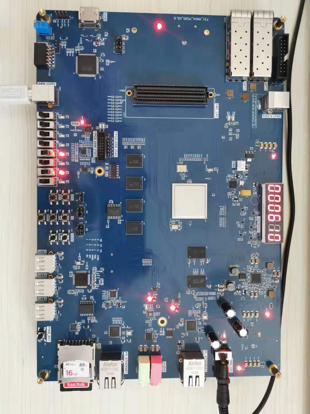
Figure 7.5 Experimental phenomenon of hexadecimal number to BCD code conversion
Experiment 8 Use of ROM
8.1 Experiment Objective
- Study the usage of internal memory block of FPGA
- Study the format of *.coe and how to edit *.coe file to configure the contents of ROM
- Learn to use RAM, read and write RAM
8.2 Experiment Implement
- Design 16 outputs ROM, address ranging 0-255
- Interface 8-bit switch input as ROM’s address
- Segment display illustartes the contents of ROM and require conversion of hexadecimal to BCD output.
8.3 Experiment
8.3.1 Program Design
The first step: the establishment of the main program framework (interface design)
| module rom_test(
input inclk_p, input inclk_n, input rst, input [7:0] sw, output reg [7:0] tube_sel, output reg [5:0] tube_seg ); endmodule |
The second step: call ROM IP core
Refer to experiment 1 and experiment 6, select Block Memory Generator, double-click to enter the setting interface, as shown in Figure 8.1, and set according to the parameters in the figure.
In the Basic window, as shown in Figure 8.1:
- Component Name: Component
- Memory Type: Signal Port ROM
- Others set as default
In the Port A Options window, as shown in Figure 8.2.
- Poart A Width: 16
- Poart A Depth: 256
- Enable Port Type: Always Enabled
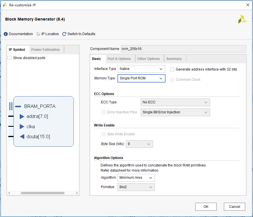
Figure 8.1 ROM setting 1
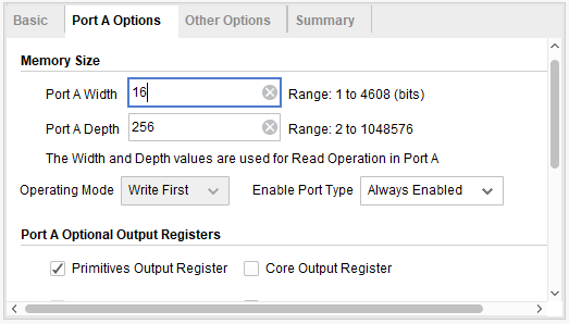
Figure 8.2 ROM setting 2
Click OK button to generate ROM
The third step: instantiate ROM
| reg [15:0] rom_q;
rom_256x16 rom_256x16_inst ( .clka (sys_clk), .addra (sw), .douta (rom_q) ); |
The fourth step: create *.coe file and initialize ROM
The .coe file for this experiment was generated based on matlab2018. The *.m file is as follows:
| % –by Alex li–
% function : create .coe clear all; close all; clc; depth= 256; width =16; fid_s = fopen(‘test_rom.coe’, ‘w+’); fprintf(fid_s, ‘MEMORY_INITIALIZATION_RADIX = %d;\n’,width); fprintf(fid_s, ‘%s\n’, ‘MEMORY_INITIALIZATION_VECTOR =’); for i=0:depth–1 data =i*i; b=dec2hex(data); fprintf(fid_s, ‘%s’, b); fprintf(fid_s, ‘%s\n’, ‘,’); end fclose(fid_s); disp(‘=======mif file completed========’); |
The generated *.m file has a depth of 256, the width of each data is 16, and the data is the square of the depth value. *.coe file content and format are shown in Figure 8.3.
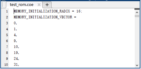
Figure 8.3 *.coe file content
Under the Sources window of the Vivado interface, expand the Design Sources folder, double-click to open the ROM created previously, enter the setting interface, under the Other Options window, select the check box Load Init Flie, and click Browse to add the generated *.coe file, such as shown in Figure 8.4, click the OK button to complete the initialization of the ROM.
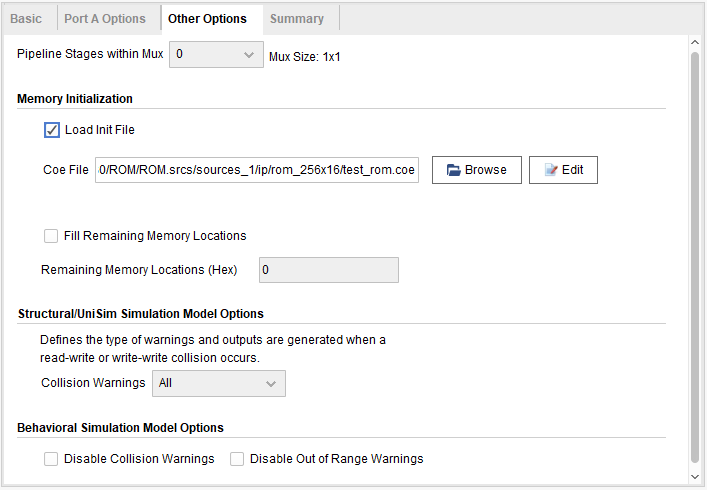
Figure 8.4 Initialize ROM
The fifth step: comprehensive design
Instantiate all modules and integrate them into the top-level file. Refer to experiment 7 to complete the program design.
8.4 Experiment Verification
The first step: add constraints and assign pins
The pin assignment is the same as that of experiment 7, refer to experiment 7 for more information.
The second step: run the implementation, generate bitstream files, and verify the board
After successfully downloading the generated programmable bitstream file to the Zynq_7030 development board, the experimental phenomenon is shown in Figure 8.5.
When the DIP switch is 0000_0011 (3 in decimal), which means the content in the third byte of the rom will be read out. The segment display illustartes 9 and is the square of 3, which is consistent with the data have been stored.
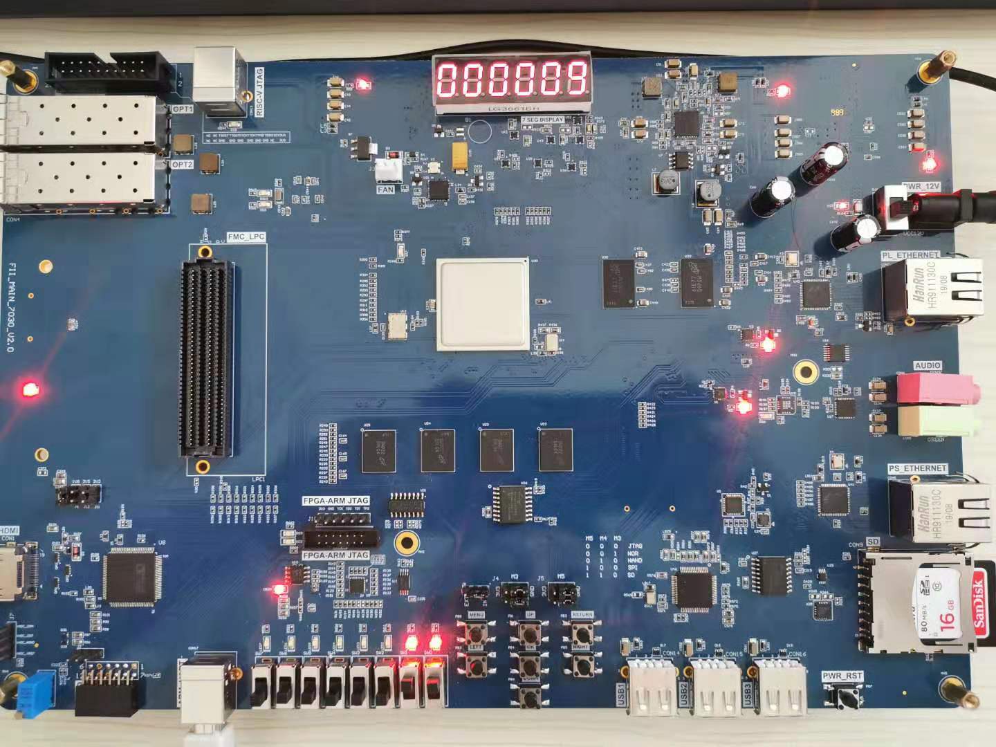
Figure 8.5 Experimental phenomenon of ROM usage
Experiment 9 Use Dual-port RAM to Read and Write Frame Data
9.1 Experiment Objective
- Learn to configure and use dual-port RAM
- Learn to use synchronous clock to control the synchronization of frame structure
- Learn to use asynchronous clock to control the synchronization of frame structure
- Use ILA to observe the structure of a synchronized clock frame
- Extended the use of dual-port RAM
- Design the use of three-stage state machine
Experiment Implement
- Use ILA to observe the structure of a synchronized clock frame
- Extended the use of dual-port RAM
- Design the use of three-stage state machine
- Design a 16-bit data frame
- Data is generated by an 8-bit counter: Data={~counta,counta}
- The ID of the data frame inputted by the switch (7 bits express maximum of 128 different data frames)
- 16-bit checksum provides data verification
- 16-bit checksum accumulates, discarding the carry bit
- After the checksum is complemented, append to the frame data
- Provide configurable data length data_len by parameter
- Packet: When the data and checksum package are written to the dual-port RAM, the userID, the frame length and the valid flag are written to the specific location of the dual-port RAM. The structure of the memory is shown in Table 9.1.
Table 9.1 Memory structure
| Wr_addr | Data/ Flag | Rd_addr |
| 8’hff | {valid,ID,data_len} | 8’hff |
| … | N/A | … |
| 8’hnn+2 | N/A | 8’hnn+2 |
| 8’hnn+1 | ~checksum+1 | 8’hnn+1 |
| 8’hnn | datann | 8’hnn |
| … | …. | … |
| 8’h01 | Data1 | 8’h01 |
| 8’h00 | Data0 | 8’h00 |
- Read and write in an agreed order
valid is the handshake signal. This flag provides the possibility of read and write synchronization, so the accuracy of this signal must be ensured in the program design.
9.3 Experiment
9.3.1 Program Introduction
The first step: the establishment of the main program framework (interface design)
| module frame_ram
#(parameter data_len=250) ( input inclk_p, input inclk_n, input rst, input [6:0] sw, output reg [6:0] oID, output reg rd_done, output reg rd_err ); |
The second step: definition of state machine
| parameter [2:0] mema_idle=0,
mema_init=1, mema_pipe0=2, mema_read0=3, mema_read1=4, mema_wr_data=5, mema_wr_chsum=6, mema_wr_done=7; parameter [2:0] memb_idle=0, memb_init=1, memb_pipe0=2, memb_read0=3, memb_read1=4, memb_rd_data=5, memb_rd_chsum=6, memb_rd_done=7; |
The third step: definition of others
| Clock variable definition
wire sys_clk; wire BCD_clk; wire sys_rst; reg ext_clk; Dual-port RAM interface definition reg [7:0] addr_a; reg [15:0] data_a; reg wren_a; wire [15:0] q_a; reg [7:0] addr_b; reg wren_b; wire [15:0] q_b; Write state machine part variable definition reg [6:0] user_id; reg [7:0] wr_len; reg [15:0] wr_chsum; wire wr_done; reg [7:0] counta; wire [7:0] countb; assign countb=~counta; reg [15:0] rd_chsum; reg [7:0] rd_len; reg [15:0] rd_data; reg ext_rst; reg [2:0] sta; reg [2:0] sta_nxt,; Read state machine part variable definition reg [15:0] rd_chsum; reg [7:0] rd_len; reg [15:0] rd_data; reg [2:0] stb; reg [2:0] stb_nxt; |
The fourth step: genertae dual-port RAM, PLL
| dp_ram dp_ram_inst
( .address_a (addr_a), .address_b (addr_b), .clock (sys_clk), .data_a (data_a), .data_b (16’b0), .wren_a (wren_a), .wren_b (wren_b), .q_a (q_a), .q_b (q_b) ); pll_sys_rst pll_sys_rst_inst ( .inclk (inclk), .sys_clk (sys_clk), .BCD_clk (BCD_clk), .sys_rst (sys_rst) ); |
The RAM is 16 bits wide and 256 in depth. The PLL inputs a 50MHz clock and outputs 100MHz as the working clock of other modules, and 20MHz is used to drive the segment display.
The fifth step: data generation counter
| always @ (posedge sys_clk)
if(sys_rst) begin counta <= 0; user_id <= 0; end else begin counta <=counta + 1; user_id <= sw; end |
The sixth step: write state machine
| assign wr_done = (wr_len == (data_len – 1’b1));
//Think why using wr_len==data_len-1, instead of wr_len==data_len //First stage always @ (posedge sys_clk) begin if (sys_rst) begin sta = mema_idle; end else sta = sta_nxt; end //Second stage always @ (*) begin case (sta) mema_idle : sta_nxt = mema_init; mema_init : sta_nxt = mema_pipe0; mema_pipe0 : sta_nxt = mema_read0; mema_read0 : begin if (!q_a[15]) sta_nxt = mema_read1; else sta_nxt = sta; end mema_read1 : begin if (!q_a[15]) sta_nxt = mema_wr_data; else sta_nxt = sta; end mema_wr_data : begin if (wr_done) sta_nxt = mema_wr_chsum; else sta_nxt = sta; end mema_wr_chsum : sta_nxt = mema_wr_done; mema_wr_done : sta_nxt = mema_init; default : sta_nxt = mema_idle; endcase end |
| //Third stage
always @ (posedge sys_clk) begin case (sta) mema_idle : begin addr_a <= 8’hff; wren_a <= 1’b0; data_a <= 16’b0; wr_len <= 8’b0; wr_chsum <= 0; end mema_init, mema_pipe0, mema_read0, mema_read1 : begin addr_a <= 8’hff; wren_a <= 1’b0; data_a <= 16’b0; wr_len <= 8’b0; wr_chsum <= 0; end mema_wr_data : begin addr_a <= addr_a + 1’b1; wren_a <= 1’b1; data_a <= {countb, counta}; wr_len <= wr_len + 1’b1; wr_chsum <= wr_chsum + {countb, counta}; end mema_wr_chsum : begin addr_a <= addr_a + 1’b1; wr_len <= wr_len + 1’b1; wren_a <= 1’b1; data_a <= (~wr_chsum) + 1’b1; end mema_wr_done : begin addr_a <= 8’hff; wren_a <= 1’b1; data_a <= {1’b1, user_id, wr_len}; end default : ; endcase end |
Write order:
- Read the flag of the 8’hff address (control word). If valid=1’b0, the program proceeds to the next step, otherwise waits
- Address plus 1, 8’hff+1 is exactly zero, write data from 0 address and calculate the checksum
- Determine whether the interpretation reaches the predetermined data length. If so, proceeds to next step, otherwise the data is written, and the checksum is calculated.
- checksum complements and write to memory
- Write the control word in the address 8’hff, packet it
The sevneth step: read state machine
| //first stage
always @ (posedge sys_clk) begin if (!ext_rst) begin stb = memb_idle; end else stb = stb_nxt; end //second stage always @ (*) begin case (stb) memb_idle : stb_nxt = memb_init; memb_init : stb_nxt = memb_pipe0; memb_pipe0 : stb_nxt = memb_read0; memb_read0 : begin if (q_b[15]) stb_nxt = memb_read1; else stb_nxt = memb_init; end memb_read1 : begin if (q_b[15]) stb_nxt = memb_rd_data; else stb_nxt = memb_init; end memb_rd_data : begin if(rd_done) stb_nxt = memb_rd_chsum; else stb_nxt = stb; end memb_rd_chsum : stb_nxt = memb_rd_done;
memb_rd_done : stb_nxt = memb_init; default : stb_nxt = memb_idle; endcase end |
| // Third stage, the actual operation needs to be driven by the edge of the clock.
always @ (posedge sys_clk) begin case (stb) memb_idle : begin addr_b <= 8’hff; rd_data <= 0; rd_chsum <= 0; wren_b <= 1’b0; rd_len <= 8’b0; oID <= 7’b0; rd_err <= 1’b0; end memb_init : begin addr_b <= 8’hff; rd_data <= 0; rd_chsum <= 0; wren_b <= 1’b0; rd_len <= 8’b0; oID <= 7’b0; rd_err <= 1’b0; end memb_pipe0 : begin addr_b <= 8’b0; end memb_read0 : begin if (q_b[15]) addr_b <= addr_b + 1’b1; else addr_b <= 8’hff; rd_data <= 0; rd_chsum <= 0; wren_b <= 1’b0; rd_len <= 8’b0; oID <= 7’b0; end memb_read1 : begin if(q_b[15]) addr_b <= addr_b + 1’b1; else addr_b <= 8’hff; rd_data <= 0; rd_chsum <= 0; wren_b <= 1’b0; rd_len <= q_b[7:0]; oID <= q_b[14:8]; end memb_rd_data : begin addr_b <= addr_b + 1’b1; rd_data <= q_b; rd_chsum <= rd_chsum + rd_data; wren_b <= 1’b0; rd_len <= rd_len – 1’b1; end memb_rd_chsum : begin addr_b <= 8’hff; wren_b <= 1’b0; if (|rd_chsum) rd_err <= 1’b1; end memb_rd_done : begin addr_b <= 8’hff; wren_b <= 1’b1; end default : ; endcase end |
Read order
- idle is the state after reset
- Init: Initialization, set the address to 8’hff
- Rd_pipe0: Add a latency (since the read address and data are both latched). Address +1, forming a pipeline structure
- Read0: Set the address to 8’hff, read the control word and judge whether the valid bit is valid.
- If valid=1’b1, address +1, proceeds to the next step
- If valid=1’b0, it means the packet is not ready yet, the address is set to be 8’hff and returns to the init state.
- Read1: Read the control word again
- If valid=1’b1, address+1, ID and data length are assigned to the corresponding variables and proceeds to the next step
- If valid=1’b0, it means the packet is not ready yet, the address is set to 8’hff, and returns to the init state.
- Rd_data:
- Read data and pass to data variables
- Calculate checksum, data_len – 1
- Determine whether the data_len is 0
- 0: all data has been read, proceeds to the next step
- Not 0: continue the operation in current state
- rd_chsum: Read the value of checksum and calculate the last checksum. Correct the data and set the flag of rd_err
- rd_done: The last step clears the valid flag in memory and opens the write enable for the next packet.
9.4 Experiment Verification
The first step: add constraints and assign pins
The pin assignment is shown in Table 9.1.
Table 9.1 Dual-port RAM read an dwrite fram data experiment pin mapping table
| Signal Name | Network Name | FPGA Pin | Port Description |
| inclk_p | SYSCLK_P | AC13 | Input clock(differental)
200MHz |
| inclk_n | SYSCLK_N | AD13 | |
| rst | GPIO_SW_2 | F4 | Reset |
| sw[0] | GPIO_DIP_SW0 | A17 | 8-bit switch |
| sw[1] | GPIO_DIP_SW1 | E8 | |
| sw[2] | GPIO_DIP_SW2 | C6 | |
| sw[3] | GPIO_DIP_SW3 | B9 | |
| sw[4] | GPIO_DIP_SW4 | B6 | |
| sw[5] | GPIO_DIP_SW5 | H6 | |
| sw[6] | GPIO_DIP_SW6 | H7 | |
| oID[0] | SEF_PA | J10 | 7-bit LED
(segment display) Indicate output address |
| oID[1] | SEF_PB | J9 | |
| oID[2] | SEF_PC | A7 | |
| oID[3] | SEF_PD | B7 | |
| oID[4] | SEF_PE | A8 | |
| oID[5] | SEF_PF | A9 | |
| oID[6] | SEF_PG | A10 | |
| rd_err | GPIO_DIP_SW7 | G9 | Read error signal |
| rd_done | SEF_DP | B10 | Read end signal |
The second step: observe the read and write results of the dual-port RAM with ILA
- In order to facilitate the observation of the read and write state machine synergy results, the data length is changed to 4 here, recompile and download. Users can test themselves using long data
| module frame_ram
#(parameter data_len=4) ( input inclk_p, input inclk_n input rst, input [6:0] sw, output reg [6:0] oID, output reg rd_done, output reg rd_err ); |
- Observe the simulation result
- Observe the handshake mechanism through dual-port RAM
- Determine whether the reading is started after the packet is written
- Determine whether the write packet is blocked before reading the entire packet is completed.
- Observe the external interface signal and status
- rd_done, rd_err
Set rd_err = 1, or the rising edge is the trigger signal to observe whether the error signal is captured.
- Observe whether wren_a, wren_b signal and the state machine jump are strictly matched to meet the design requirements.
- ILA result, see Figure 9.1.
The third step: run the implementation, generate bitstream files, and verify the board
After successfully downloading the generated programmable bitstream file to the Zynq_7030 development board, the experimental phenomenon is shown in Figure 9.1.
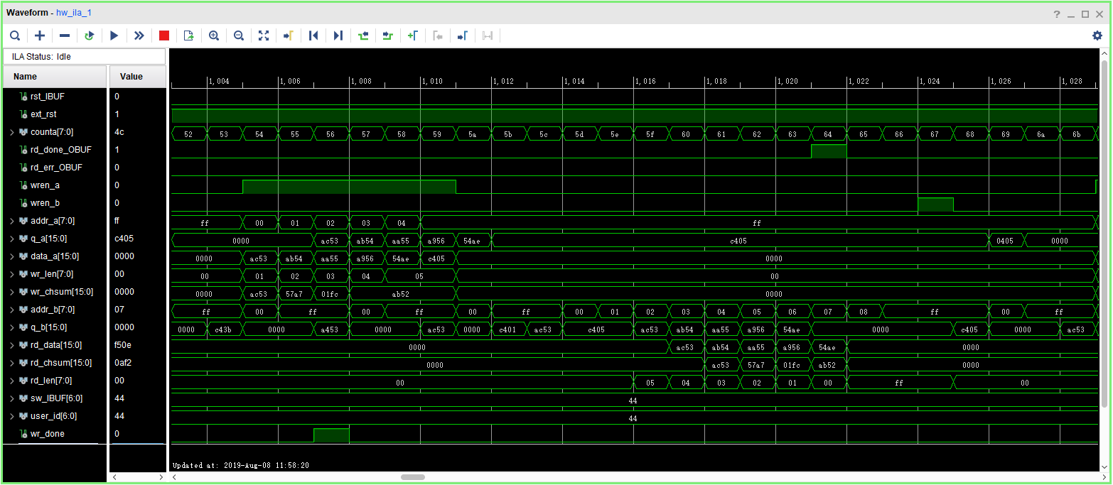
Figure 9.1 Experimental phenomenon
9.5 Experiment Summary and Reflection
- Review the design requirements. How to analyze an actual demand, to gradually establish a model of digital control and state machine and finally design.
- Modify the third stage of the state machine into the if…else model and implement.
- Focus on thinking If the read and write clocks are different. After it becomes an asynchronous mechanism, how to control the handshake.
- According to the above example, consider how dual-port RAM can be used in data acquisition, asynchronous communication, embedded CPU interface, and DSP chip interface.
- How to build ITCM with dual-port RAM and DTCM preparing for future CPU design.
Experiment 10 Asynchronous Serial Port Design and Experiment
10.1 Experiment Objective
Because asynchronous serial ports are very common in industrial control, communication, and software debugging, they are also vital in FPGA development.
- Study the basic principles of asynchronous serial port communication, handshake mechanism, data frame
- Master asynchronous sampling techniques
- Review the frame structure of the data packet
- Learning FIFO
- Joint debugging with common debugging software of PC (SSCOM, teraterm, etc.)
10.2 Experiment Implement
- Design and transmit full-duplex asynchronous communication interface Tx, Rx
- Baud rate of 11520 bps, 8-bit data, 1 start bit, 1 or 2 stop bits
- Receive buffer (Rx FIFO), transmit buffer (Tx FIFO)
- Forming a data packet
- Packet parsing
10.3 Experiment
10.3.1 USB to Serial Chip (FT2232) Introduction
USB is an interface technology used in the PC field to regulate the connection and communication between computers and external devices. The USB interface supports plug-and-play and hot-swap capabilities of the device, and can connect up to 127 peripherals, such as a mouse, modem, and keyboard. However, there are still a large number of peripheral devices and software using the RS232 serial port standard. In order to take full advantage of USB, a USB-RS232 converter is designed to transmit RS232 data through the USB bus. Here, a design scheme of USB-RS232 conversion module based on FT2-232H is proposed.
The on-board serial conversion chip is FT2232, which can implement USB to two serial UART, FIFO, Bit-Bang I/O interfaces, and can also be configured as MPSSE, I2C, JTAG and SPI buses. FT2232H has 2 independent UART / FIFO controllers for controlling asynchronous data, 245 FIFO data, optical isolation (high-speed serial port) or controlling Bit-Bang mode when installing program commands; The USB protocol engine controls and manages the interface between UTMI PHY and FIFO, and is responsible for power management and USB protocol specifications; the dual-port FIFO TX buffer (4KB) stores data from the host PC and uses the data through the multi-purpose UART and FIFO controller; the dual-port FIFO RX buffer (4KB) stores the data from the multi-purpose UART / FIFO controller, and then sends the data to the host; when the reset generator module is powered on, it provides a reliable power supply reset for the internal circuit of the device. The RESETn input pin allows external devices to reset the FT2232H. If RESETn is not used, it should be connected to VCCIO (+3.3 V); the independent baud rate generator provides a × 16 or × 10 clock signal to the UART. It provides the best baud rate tuning through a 14-bit scale factor and 4 registered bits, which determines the baud rate programmable by the UART.
10.3.2 Hardware Design
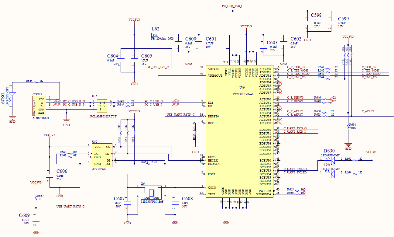
Figure 10.1 Schematics of serial port
The principle of USB serial port conversion is shown in Figure 10.1. CON17 is a USB interface. When downloading the program, it is input to the FT2232 through the two wires PC_C_USB_R_N and PC_C_USB_R_P. After internal processing, it is input into the FPGA by C_UART_TXD_O. In the serial port experiment, the sending path from the PC to the FPGA is the same as the download program path. The receiving path from the FPGA to the PC is the FPGA transmitting data from C_UART_RXD_I to the FT2232. After internal processing, the data is sent to the PC through the USB interface to achieve serial communication receive and send.
10.3.3 Program Introduction
The first step: the establishment of the main program framework (interface design)
| module uart_top
( input inclk_p, input inclk_n, input rst, input [1:0] baud_sel, input tx_wren, input tx_ctrl, input [7:0] tx_data, input tx_done, output txbuf_rdy,
input rx_rden, output [7:0] rx_byte, output rx_byte_rdy, output sys_rst, output sys_clk, input rx_in, output tx_out ); |
There are a lot of handshake signals here, with the tx prefix for the transmit part of the signal, and the rx prefix is for the receive part of the signal.
The second step: create a new baud rate generator file
- Input clock 7.3728MHz (64 times 115200). The actual value is 7.377049MHz, which is because the coefficient of the PLL is an integer division, while the error caused by that is not large, and can be adjusted by the stop bit in asynchronous communication. See Figure 10.2.
Fine solution
- Implemented with a two-stage PLL for a finer frequency
- The stop bit is set to be 2 bits, which can effectively eliminate the error. (This experiment will not deal with the precision.)
- Support output baud rate 115200, 57600, 38400, 19200
- The default baud rate is 115200
- Source file designing baud rate
| // Send baud rate, clock frequency division selection
wire [8:0] frq_div_tx; assign frq_div_tx = (baud_sel == 2’b00) ? 9’d63: (baud_sel == 2’b01) ? 9’d127: (baud_sel == 2’b10) ? 9’d255:9’d511; reg [8:0] count_tx=9’d0; always @ (posedge inclk) if (!rst) begin count_tx <= 9’d0; baud_tx <= 1’b0; end else begin if (count_tx == frq_div_tx) begin count_tx <= 9’d0; baud_tx <= 1’b1; end else begin count_tx <= count_tx + 1’b1; baud_tx <= 1’b0; end end |
Four different gear positions are set to select the baud rate, corresponding to the second step, (1). The baud rate of the receiving part is similar to that of the transmitting part.
Step 3: Design the send buffer file tx_buf
- 8-bit FIFO, depth is 256, read/write clock separation, write full flag, read empty flag
- Interface and handshake
- rst reset signal
- wr_clk write clock
- tx_clk send clock
- 8-bit write data tx_data
- wr_en write enable
- ctrl writes whether the input is a data or a control word
- rdy buffer ready, can accept the next data frame
Transmit buffer instantiation file
| tx_buf
#(.TX_BIT_LEN(8),.STOP_BIT(2)) tx_buf_inst ( .sys_rst (sys_rst), .uart_rst (uart_rst), .wr_clk (sys_clk), .tx_clk (uart_clk), .tx_baud (tx_baud), .tx_wren (tx_wren), .tx_ctrl (tx_ctrl), .tx_datain (tx_data), .tx_done (tx_done), .txbuf_rdy (txbuf_rdy), .tx_out (tx_out) ); |
- Serial transmission, interface and handshake file design
- Interface design
- tx_rdy, send vacancy, can accept new 8-bit data
- tx_en, send data enable, pass to the sending module 8-bit data enable signal
- tx_data, 8-bit data to be sent
- tx_clk, send clock
- tx_baud, send baud rate
- Instantiation
| tx_transmit
#(.DATA_LEN(TX_BIT_LEN), .STOP_BIT(STOP_BIT) ) tx_transmit_inst ( .tx_rst (uart_rst), .tx_clk (tx_clk), .tx_baud (tx_baud), .tx_en (tx_en), .tx_data (tx_data), .tx_rdy (trans_rdy), .tx_out (tx_out) ); |
- Write a testbench file to simulate the transmit module. (uart_top_tb)
- Transmit part of the ModelSim simulation waveform, as shown in Figure 10.2.
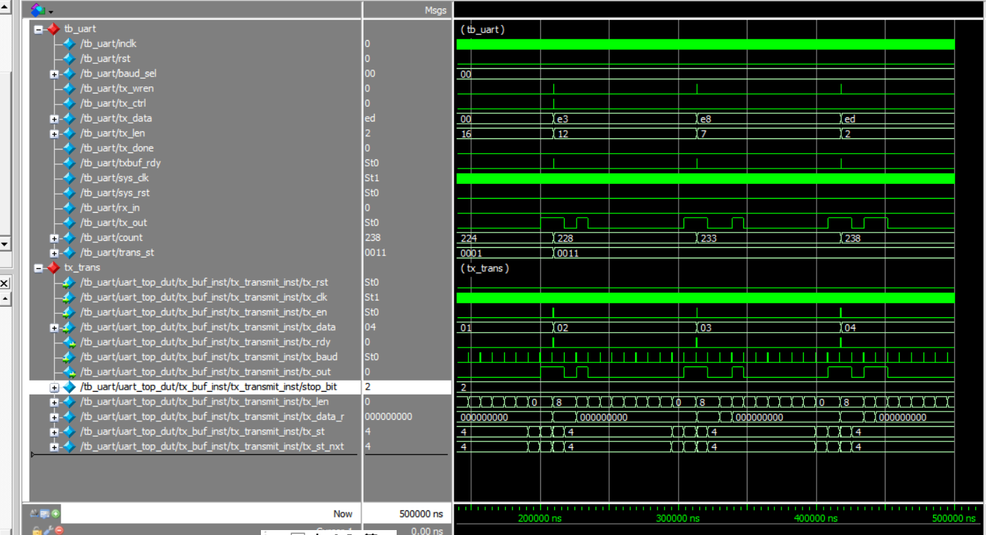
Figure 10.2 Serial port sends MoselSim simulation waveform
- Extended design (extended content is only reserved for users to think and practice)
- Design the transmitter to support 5, 6, 7, 8-bit PHY (Port physical layer)
- Support parity check
- The settings of the above steps involve FIFO, PLL, etc. (Refer to uart_top project file)
The fourth step: UART receiving module design
- Design of rx_phy.v
- Design strategies and steps
- Use 8 times sampling: so rx_baud is different from tx_baud, here sampling is rx_band = 8*tx_band
- Adopting judgments to the receiving data
Determine whether the data counter is greater than 4 after the sampling value is counted.
- Steps to receive data:
- Synchronization: refers to how to find the start bit from the received 0101 (sync_dtc)
- Receive start bit (start)
- Cyclically receive 8-bit data
- Receive stop bit (determine whether it is one stop bit or two stop bits)
- Determine if the stop bit is correct
- Correct, jump to step B
- Incorrect, jump to step A, resynchronize
- Do not judge, jump directly to B, this design adopts the scheme of no judgment
- Design of rx_buf
- Design strategies and steps
- Add 256 depth, 8-bit fifo
- Read and write clock separation
- Asynchronous clear (internal synchronization)
- Data appears before the rdreq in the read port
- Steps:
- Initialization: fifo, rx_phy
- Wait: FIFO full signal (wrfull) is 0
- Write: Triggered by rx_phy_byte, rx_phy_rdy of rx_phy:
- End of writing
- Back to step b and continue to wait
- rx_buf.v source program (Reference to project files)
- Receive module simulation
Content and steps
- tx, rx loopback test (assign rx_in = tx_out)
- Continue to use the testbench file in the TX section
- Write the testbench of rx
- ModelSim simulation. See Figure 10.3.
- Reflection and development
- Modify the program to complete the 5, 6, 7, 8-bit design
- Completing the design of the resynchronization when the start and stop have errors of the receiving end rx_phy
- Complete the analysis and packaging of the receiving data frame of rx_buf
- Using multi-sampling to design 180° alignment data sampling method, compare FPGA resources, timing and data recovery effects
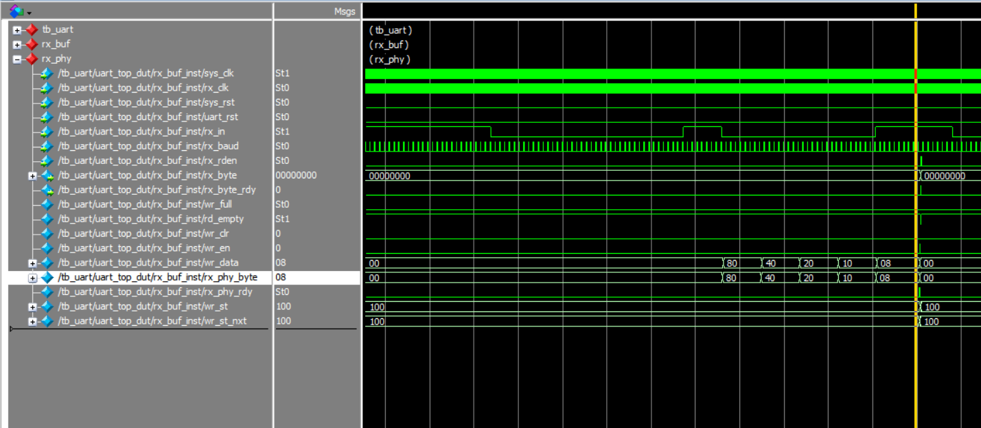
Figure 10.3 rx_phy waveform
10.4 Experiment Verification
- Hardware interface, Zynq_7030 development board has integrated USB to serial port conversion
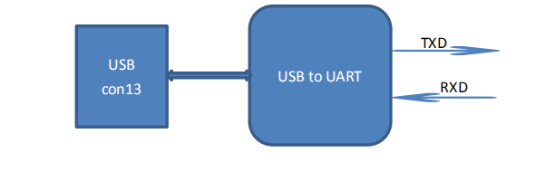
- Write a hardware test file
- Test plan: connect development board CON13 to host USB interface
- Using test software such as teraterm, SSCOM3, etc., you can also write a serial communication program (C#, C++, JAVA, Python…)
- PC sends data in a certain format
- The test end uses a counter to generate data in a certain format.
- Write the test program uart_hw_test and instantiate uart_top in it.
- Set uart_hw_test to the top level, instantiate the previous program, and then verify it
- Pin assignmnets:
Assign pins: shown in Table 10.1.
Table 10.1 Serial port experimental pin mapping table
| Signal Name | Network Name | FPGA Pin | Port Description |
| inclk_p | SYSCLK_P | AC13 | Input clock(differential)
200MHz |
| inclk_n | SYSCLK_N | AD13 | |
| rst | GPIO_SW_2 | F4 | Reset |
| rx_in | FPGA_RXI | AC26 | Serial data input signal |
| tx_out | FPGA_TXO | ZE22 | Serial data output signal |
- Experiment phenomenon: observe the data received by the PC. See Figure 10.4.
Figure 10.4 Sent data received on the host computer
Experiment 11 IIC Protocol Transmission
11.1 Experiment Objective
- Learning the basic principles of asynchronous IIC bus, and the IIC communication protocol
- Master the method of reading and writing EEPROM
- Joint debugging using logic analyzer
11.2 Experiment Implement
- Correctly write a number to any address in the EEPROM (this experiment writes to the register of 8’h03 address) through the FPGA (here changes the written 8-bit data value by (SW7~SW0)). After writing in successfully, read the data as well. The read data is displayed directly on the segment display.
- Download the program into the FPGA and press the left push button to execute the data write into EEPROM operation. Press the right push button to read the data that was just written.
- Determine whether it is correct or not by reading the displayed number on the segment display. If the segment display has the same value as written value, the experiment is successful.
- Analyze the correctness of the internal data with ILA and verify it with the display of the segment display.
11.3.1 Introduction to EEPROM and IIC Protocol
- EEPROM Introduction
EEPROM (Electrically Erasable Programmable Read Only M emory) refers to a charged erasable programmable read only register. It is a memory chip that does not lose data after turning off power.
On the experiment board, there is an IIC interface EEPROM chip M24C08 with a capacity of 1024 bytes. Users can store some hardware configuration data or user information due to the characteristics that the data is not lost after power-off.
- The overall timing protocol of IIC is as follows:
- Bus idle state: SDA, SCL are high
- Start of IIC protocol: SCL stays high, SDA jumps from high level to low level, generating a start signal
- IIC read and write data stage: including serial input and output of data and response signal issued by data receiver
- IIC transmission end bit: SCL is in high level, SDA jumps from low level to high level, and generates an end flag. See Figure 11.1.
- SDA must remain unchanged when SCL is high. It changes only when SCL is low
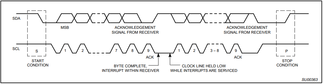
Figure 11.1 Timing protocol of IIC
11.3.2 Hardware Introduction
Each IIC device has a device address. When some device addresses are shipped from the factory, they are fixed by the manufacturer (the specific data can be found in the manufacturer’s data sheet). Some of their higher bits are determined, and the lower bits can be configured by the user according to the requirement. The higher four-bit address of the EEPROM chip M24C08 used by the develop board has been fixed to 1010 by the component manufacturer. The lower three bits are linked in the develop board as shown below, so the device address is 1010000. See Figure 11.2.
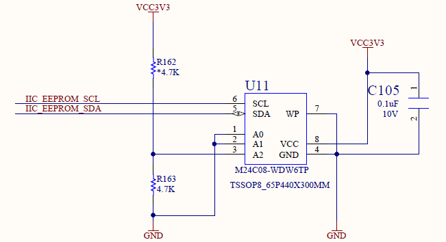
Figure 11.2 IIC schematics EEPROM part
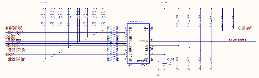
Figure 11.3 IIC SWITCH schematics
EEPROM reads and writes data through the IIC_EEPROM_SCL clock line and the IIC_EEPROM_SDA data line with the FPGA.
Because there are many on-board IIC devices, to save I / O resources of FPGA, PCA9548 chip is used as IIC SWITCH, as shown in Figure 11.3. The FPGA uses IIC_SCL_MAIN and IIC_SDA_MAIN as IIC buses to connect to PCA9548, and then passes PCA9548 to drive IIC devices. It can drive up to 8 IIC devices at the same time and itself is driven by the IIC protocol.
11.3.3 Program Introduction
This experiment has two main modules, I2C reading and writing module and LED display module; The first module is mainly introduced here.
The first step: establishment of the main program framework
| eeprom_test(
input inclk_p, input inclk_n, input rst, input key_wr, input key_rd, input [7:0] sw, output tube_sel1, output tube_sel2, output [7:0] tube_seg, inout scl, inout sda ); |
Inputs are differential clock, reset signal rst, write control signal key_wr, read control signal key_rd, and write content are controlled by switch SW. The output signals are two segment display selection signals tube_sel1, tube_sel2, segment selection signal tube_seg, and a set of IIC bus scl clock lines and sda data lines.
The second step: create clock IIC_CLK
| reg [2:0] cnt;
reg [8:0] cnt_delay; reg scl_r; reg scl_link ; always @ (posedge clk or posedge rst) begin if (rst) cnt_delay <= 9’d0; else if (cnt_delay == 9’d499) cnt_delay <= 9’d0; else cnt_delay <= cnt_delay + 1’b1; //10us end always @ (posedge clk or posedge rst) begin if (rst) cnt <= 3’d5; else begin case (cnt_delay) 9’d124: cnt <= 3’d1; //cnt=1:scl 9’d249: cnt <= 3’d2; //cnt=2:scl 9’d374: cnt <= 3’d3; //cnt=3:scl 9’d499: cnt <= 3’d0; //cnt=0:scl default: cnt<=3’d5; endcase end end `define SCL_POS (cnt==3’d0) //cnt=0:scl `define SCL_HIG (cnt==3’d1) //cnt=1:scl `define SCL_NEG (cnt==3’d2) //cnt=2:scl `define SCL_LOW (cnt==3’d3) //cnt=3:scl always @ (posedge clk or posedge rst) begin if (rst) scl_r <= 1’b0; else if (cnt == 3’d0) scl_r <= 1’b1; else if (cnt == 3’d2) scl_r <= 1’b0; end assign scl = scl_link ? scl_r : 1’bz; |
First, divide 50MHz system clock to obtain a 100KHz clock with a period of 10us as the transmission clock of the I2C protocol, and then use the counter to define the rising edge, high state, falling edge and low state of the clock to prepare for subsequent data reading and writing and the start and end of the I2C protocol. The last sentence means to define a data valid signal. Only when the signal is high, that is, when the data is valid, the I2C clock is valid again, otherwise it is in a high impedance state. This is also set in accordance with the I2C transmission protocol.
The third step: specific implementation of I2C transmission
| `define DEVICE_READ 8’b1010_0001
`define DEVICE_WRITE 8’b1010_0000 `define BYTE_ADDR 8’b0000_0011 `define IIC_SWITCH_ADDR 7’b1110_000 `define EEPROM_CHANNEL 8’b0000_0001 parameter IDLE = 5’d0; parameter START0 = 5’d1; parameter ADD0 = 5’d2; parameter ACK0 = 5’d3; parameter CHANNEL = 5’d4; parameter ACK_C = 5’d5; parameter STOP0 = 5’d6; parameter START1 = 5’d7; parameter ADD1 = 5’d8; parameter ACK1 = 5’d9; parameter ADD2 = 5’d10; parameter ACK2 = 5’d11; parameter START2 = 5’d12; parameter ADD3 = 5’d13; parameter ACK3 = 5’d14; parameter DATA = 5’d15; parameter ACK4 = 5’d16; parameter STOP1 = 5’d17; parameter STOP2 = 5’d18; always @ (posedge clk or posedge rst) begin if (rst) begin cstate <= IDLE; sda_r <= 1’b1; scl_link <= 1’b1; sda_link <= 1’b1; num <= 4’d0; read_data <= 8’b0000_0000; cnt_5ms <= 20’h00000; iic_done <= 1’b0; end else case (cstate) IDLE : begin sda_link <= 1’b1; scl_link <= 1’b1; iic_done <= 1’b0 ; if (wr_en) begin db_r <= {`IIC_SWITCH_ADDR, 1’b0}; cstate <= START0; end else if (rd_en) begin db_r <= {`IIC_SWITCH_ADDR, 1’b1}; cstate <= START0; end else cstate <= IDLE; end START0 : begin if (`SCL_HIG) begin sda_link <= 1’b1; sda_r <= 1’b0; num <= 4’d0; cstate <= ADD0; end else cstate <= START0; end
ADD0 : begin if (`SCL_LOW) begin if (num == 4’d8) begin num <= 4’d0; sda_r <= 1’b1; sda_link <= 1’b0; cstate <= ACK0; end else begin cstate <= ADD0; num <= num + 1’b1; case (num) 4’d0 : sda_r <= db_r[7]; 4’d1 : sda_r <= db_r[6]; 4’d2 : sda_r <= db_r[5]; 4’d3 : sda_r <= db_r[4]; 4’d4 : sda_r <= db_r[3]; 4’d5 : sda_r <= db_r[2]; 4’d6 : sda_r <= db_r[1]; 4’d7 : sda_r <= db_r[0]; default : ; endcase end end else cstate <= ADD0; end ACK0 : begin if (`SCL_NEG) begin cstate <= CHANNEL; db_r <= `EEPROM_CHANNEL; end else cstate <= ACK0; end CHANNEL : begin if (`SCL_LOW) begin if (num == 4’d8) begin num <= 4’d0; sda_r <= 1’b1; sda_link <= 1’b0; cstate <= ACK_C; end else begin sda_link <= 1’b1; num <= num + 1’b1; case (num) 4’d0 : sda_r <= db_r[7]; 4’d1 : sda_r <= db_r[6]; 4’d2 : sda_r <= db_r[5]; 4’d3 : sda_r <= db_r[4]; 4’d4 : sda_r <= db_r[3]; 4’d5 : sda_r <= db_r[2]; 4’d6 : sda_r <= db_r[1]; 4’d7 : sda_r <= db_r[0]; default : ; endcase cstate <= CHANNEL; end end else cstate <= CHANNEL; end ACK_C : begin if (wr_en) if (`SCL_NEG) cstate <= STOP0; else cstate <= ACK_C; else if (rd_en) sda_r <= 1’b0; if (`SCL_NEG) cstate <= STOP0; else cstate <= ACK_C; end STOP0 : begin if (`SCL_LOW) begin sda_link <= 1’b1; sda_r <= 1’b0; cstate <= STOP0; end else if (`SCL_HIG) begin sda_r <= 1’b1; cstate <= START1; end else cstate <= STOP0; end
START1 : begin db_r <= `DEVICE_WRITE; if (`SCL_HIG) begin sda_link <= 1’b1; sda_r <= 1’b0; num <= 4’d0; cstate <= ADD1; end else cstate <= START1; end
ADD1 : begin if (`SCL_LOW) begin if (num == 4’d8) begin num <= 4’d0; sda_r <= 1’b1; sda_link <= 1’b0; cstate <= ACK1; end else begin cstate <= ADD1; num <= num + 1’b1; case (num) 4’d0 : sda_r <= db_r[7]; 4’d1 : sda_r <= db_r[6]; 4’d2 : sda_r <= db_r[5]; 4’d3 : sda_r <= db_r[4]; 4’d4 : sda_r <= db_r[3]; 4’d5 : sda_r <= db_r[2]; 4’d6 : sda_r <= db_r[1]; 4’d7 : sda_r <= db_r[0]; default : ; endcase end end else cstate <= ADD1; end
ACK1 : begin if (`SCL_NEG) begin cstate <= ADD2; db_r <= `BYTE_ADDR; end else cstate <= ACK1; end
ADD2 : begin if (`SCL_LOW) begin if (num == 4’d8) begin num <= 4’d0; sda_r <= 1’b1; sda_link <= 1’b0; cstate <= ACK2; end else begin sda_link <= 1’b1; num <= num+1’b1; case (num) 4’d0 : sda_r <= db_r[7]; 4’d1 : sda_r <= db_r[6]; 4’d2 : sda_r <= db_r[5]; 4’d3 : sda_r <= db_r[4]; 4’d4 : sda_r <= db_r[3]; 4’d5 : sda_r <= db_r[2]; 4’d6 : sda_r <= db_r[1]; 4’d7 : sda_r <= db_r[0]; default : ; endcase cstate <= ADD2; end end else cstate <= ADD2; end
ACK2 : begin if (`SCL_NEG) begin if (wr_en) begin cstate <= DATA; db_r <= data_tep; end else if (rd_en) begin db_r <= `DEVICE_READ; cstate <= START2; end end else cstate <= ACK2; end
START2 : begin if (`SCL_LOW) begin sda_link <= 1’b1; sda_r <= 1’b1; cstate <= START2; end else if (`SCL_HIG) begin sda_r <= 1’b0; cstate <= ADD3; end else cstate <= START2; end
ADD3 : begin if (`SCL_LOW) begin if (num == 4’d8) begin num <= 4’d0; sda_r <= 1’b1; sda_link <= 1’b0; cstate <= ACK3; end else begin num <= num + 1’b1; case (num) 4’d0 : sda_r <= db_r[7]; 4’d1 : sda_r <= db_r[6]; 4’d2 : sda_r <= db_r[5]; 4’d3 : sda_r <= db_r[4]; 4’d4 : sda_r <= db_r[3]; 4’d5 : sda_r <= db_r[2]; 4’d6 : sda_r <= db_r[1]; 4’d7 : sda_r <= db_r[0]; default: ; endcase end end else cstate <= ADD3; end
ACK3 : begin if (`SCL_NEG) begin cstate <= DATA; sda_link <= 1’b0; end else cstate <= ACK3; end
DATA : begin if (rd_en) begin if (num <= 4’d7) begin cstate <= DATA; if(`SCL_HIG) begin num <= num + 1’b1; case (num) 4’d0 : read_data[7] <= sda; 4’d1 : read_data[6] <= sda; 4’d2 : read_data[5] <= sda; 4’d3 : read_data[4] <= sda; 4’d4 : read_data[3] <= sda; 4’d5 : read_data[2] <= sda; 4’d6 : read_data[1] <= sda; 4’d7 : read_data[0] <= sda; default: ; endcase end end else if((`SCL_LOW) && (num == 4’d8)) begin num <= 4’d0; cstate <= ACK4; end else cstate <= DATA; end else if (wr_en) begin sda_link <= 1’b1; if (num <= 4’d7) begin cstate <= DATA; if (`SCL_LOW) begin sda_link <= 1’b1; num <= num + 1’b1; case (num) 4’d0 : sda_r <= db_r[7]; 4’d1 : sda_r <= db_r[6]; 4’d2 : sda_r <= db_r[5]; 4’d3 : sda_r <= db_r[4]; 4’d4 : sda_r <= db_r[3]; 4’d5 : sda_r <= db_r[2]; 4’d6 : sda_r <= db_r[1]; 4’d7 : sda_r <= db_r[0]; default: ; endcase end end else if ((`SCL_LOW) && (num==4’d8)) begin num <= 4’d0; sda_r <= 1’b1; sda_link <= 1’b0; cstate <= ACK4; end else cstate <= DATA; end end
ACK4 : begin if (wr_en) if (`SCL_NEG) cstate <= STOP1; else cstate <= ACK4; else if (rd_en) sda_r <= 1’b0; if (`SCL_NEG) cstate <= STOP1; else cstate <= ACK4; end
STOP1 : begin if (`SCL_LOW) begin sda_link <= 1’b1; sda_r <= 1’b0; cstate <= STOP1; end else if (`SCL_HIG) begin sda_r <= 1’b1; cstate <= STOP2; end else cstate <= STOP1; end
STOP2 : begin if (`SCL_NEG) begin sda_link <= 1’b0; scl_link <= 1’b0; end else if (cnt_5ms==20’h3fffc) begin cnt_5ms <= 20’h00000; iic_done <= 1; cstate <= IDLE; end else begin cstate <= STOP2; cnt_5ms <= cnt_5ms + 1’b1; end end
default: cstate <= IDLE; endcase end |
The entire process is implemented using a state machine. When reset, it is idle state, while data line sda_r is pulled high, clock and data are both valid, i.e. scl_link, sda_link are high; counter num is cleared and read_data is 0. 5ms delay counter is cleared, IIC transmission end signal Iic_done is low thus invalid.
- IDLE state: when the write enable signal wr_en is received, the write control word is assigned to the intermediate variable db_r <= {`IIC_SWITCH_ADDR, 1’b0}, or when the read enable signal rd_en is received, the write control word is also assigned to the intermediate variable db_r < = {`IIC_SWITCH_ADDR, 1’b1} and jump to START0 state;
- START1 state: pull the data line low when the clock signal is high, generating the start signal of IIC transmission, and jump to the device address state ADD0;
- Device address status ADD0: After the write control word or read control word is transmitted according to MSB (high order priority), the sda_link is pulled low causing data bus in a high impedance state, and jump to the first response state ACK0, waiting for the response signal from the slave.
- Response status ACK0: If the data line is pulled low, it proves that the slave receives the data normally, otherwise the data is not written into, and then the rewriting or stopping is decided by the user. There is no temporary judgment and processing here, jump directly to the channel selection state CHANNEL, and assign the channel selection information to the intermediate variable (this experiment needs to drive EEPROM, so channel 0 is used, that is, EEPROM_CHANNEL = 8’b0000_0001).
- Channel selection status CHANNEL: same as(3),the channel information is transmitted to the slave (PCA9548), and jumps to the response status ACK_C.
- Response state ACK_C: If it is a write operation, it will jump directly to the stop state STOP0. If it is a read operation, the host will send a non-response signal and then jump to the stop state STOP0;
- Stop state STOP0: jump directly to the start state START1;
(The previous states are the control of IIC SWITCH, PCA9548)
- Start state START1: Assign the write control word of EEPROM to the intermediate variable db_r <= `DEVICE_WRITE, pull the data line low when the clock signal is high, generate the start signal of I2C transmission, and jump to the device address state ADD1;
- Device address state ADD1: After the write control word (device address plus one bit 0) is transmitted in MSB (high order priority), pull sda_link low to release the data bus to a high-impedance state, and jump to the first response state ACK1, waiting for the response signal from the slave (EEPROM)
- The first response status ACK1: if the data line is pulled low, it proves that the slave normally receives the data, otherwise the data is not written into the EEPROM. The next decision to rewrite or stop is determined by the user. There is no temporary judgment and processing here. Directly jump to the write register address state ADD2, and assign the address where the data is written to, BYTE_ADDR, to the intermediate variable (this experiment writes data to the third register, that is, BYTE_ADDR = 0000_0011)
- Register address state ADD2: same as(9), transfer the register address to the slave and jump to the second response state ACK2
- The second response state ACK2: at this state, it is urgent to judge. If it is the write state wr_en, then it will jump to the data transmission state DATA, and at the same time, the written data will be assigned to the intermediate variable. If it is the read state rd_en, it jumps to the second start state START2 and assigns the read control word to the intermediate variable.
- The second start state START2: same as(8), generates a start signal and jumps to the read register address state ADD3.
- Read register address status ADD3: Jump to the third response status ACK3 after transferring the register address that needs to read data
- The third response state ACK3: directly jump to the data transmission state DATA. In the read state, the data to be read will be directly read out immediately following the register address.
- Data transfer status DATA: here judge is needed, if it is a read state, directly output the data, if it is a write state, the data to be written is transmitted to the data line SDA, and both states need to jump to the fourth response state ACK4
- Fourth response status ACK4: jump directly to stop transmission transition to STOP1
- Stop transmission transition STOP1: pull down the data line when the clock line is high,
- Transfer completed state STOP2: release all clock and data lines, return to the IDLE state after a 5ms delay and waits for the next transfer instruction. This is because EEPROM stipulates that the interval between two consecutive read and write operations must not be less than 5ms.
11.4 Experiment Verification
The first step: assign the pins
See Table 11.1 for the pin assignments.
Table 11.1 Pin mapping table of IIC protocol transmission experiment
| Signal Name | Network Name | FPGA Pin | Port Description |
| inclk_p | SYSCLK_P | AC13 | Input clock(differential)
200MHz |
| inclk_n | SYSCLK_N | AD13 | |
| rst | GPIO_SW_2 | F4 | Reset |
| key_wr | GPIO_SW_2 | D4 | Write operation |
| key_rd | GPIO_SW_2 | F2 | Read operation |
| sw[0] | GPIO_DIP_SW0 | A17 | 8-bit switch |
| sw[1] | GPIO_DIP_SW1 | E8 | |
| sw[2] | GPIO_DIP_SW2 | C6 | |
| sw[3] | GPIO_DIP_SW3 | B9 | |
| sw[4] | GPIO_DIP_SW4 | B6 | |
| sw[5] | GPIO_DIP_SW5 | H6 | |
| sw[6] | GPIO_DIP_SW6 | H7 | |
| sw[7] | GPIO_DIP_SW7 | G9 | |
| tube_sel1 | SEG_D0 | C1 | 0th bit of segment display |
| tube_sel2 | SEG_D0 | E3 | 1st bit of segment display |
| tube_seg[0] | SEF_PA | J10 | Segment selection signal |
| tube_seg[1] | SEF_PB | J9 | |
| tube_seg[2] | SEF_PC | A7 | |
| tube_seg[3] | SEF_PD | B7 | |
| tube_seg[4] | SEF_PE | A8 | |
| tube_seg [5] | SEF_PF | A9 | |
| tube _seg[6] | SEF_PG | A10 | |
| tube _seg[7] | SEF_DP | B10 | |
| scl | IIC_SCL_MAIN_LS | W14 | IIC clock bus |
| sda | IIC_SDA_MAIN_LS | W17 | IIC data bus |
The second step: run the implementation, generate bitstream files, and verify the board
After successfully downloading the generated programmable bitstream file to the Zynq_7030 development board, the experimental phenomenon is shown in Figure 11.3. Press the LEFT key to write the 8-bit value represented by SW7 ~ SW0 into the EEPROM, and then press the RIGHT key to read the value entered just now. The value of the write location. Observe the consistency between the value displayed by the segment display on the experiment board and the value (SW7 ~ SW0) written in the register 8’h03 of the EEPROM address (write 8’h34 in this experiment). The read value is displayed on the segmnet display.
Figure 11.3 IIC transmission experimental phenomenon
Experiment 12 HDMI Experiment
13.1 Experiment Objective
- Review IIC protocol knowledge
- Learn HDMI theory
13.2 Experiment Implement
Through the HDMI interface, different image contents are displayed on the screen.
13.3 Experiment
13.3.1 Introduction to HDMI Interface and ADV7511 Chip
Image display processing has always been the focus of FPGA research. At present, the image display mode is also developing. The image display interface is also gradually transitioning from the old VGA interface to the new DVI or HDMI interface. HDMI (High Definition Multimedia Interface) is a digital video/audio interface technology. It is a dedicated digital interface for image transmission. It can transmit audio and video signals at the same time.
The ADV7511 is a chip that converts FPGA digital signal to HDMI signal following VESA standard. For more details, see the related chip manual. Among them, “ADV7511 Programming Guide” and “ADV7511 Hardware Users Guide” are the most important. The registers of the ADV7511 can be configured by referring those documents.
ADV7511 Register Configuration Description: The bus inputs D0-D3, D12-D15, and D24-D27 of the ADV7511 have no input, and each bit of data is in 8-bit mode. Directly set 0x15 [3:0]) 0x0 data, 0x16 [3:2] data does not need to be set for its mode. Set [5:4] of 0X16 to 11for 8-bit data and keep the default values for the other digits. 0x17[1] refers to the ratio of the length to the width of the image. It can be set to 0 or 1. The actual LCD screen will not change according to the data, but will automatically stretch the full screen mode according to the LCD’s own settings. 0x18[7] is the way to start the color range stretching. The design is that RGB maps directly to RGB, so it can be disabled directly. 0X18[6:5] is also invalid currently. 0XAF[1] is to set HDMI or DVI mode, the most direct point of HDMI than DVI is that HDMI can send digital audio data and encrypted data content. This experiment only needs to display the picture, and it can be set directly to DVI mode. Set 0XAF[7] to 0 to turn off HDMI encryption. Due to GCCD, deep color encryption data is not applicable, so the GC option is turned off. 0x4c register does not need to be set as well. Other sound data setting can be ignored here for DVI output mode. After writing these registers, the image can be displayed successfully.
13.3.2 Hardware Design
The onboard HDMI module consists of an HDMI interface and an ADV7511 chip. The actual picture is shown in Figure 12.1. The schematic is shown in Figure 12.2.
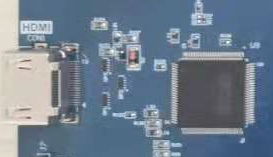
Figure 12.1 Physical picture of HDMI interface and ADV7511 chip
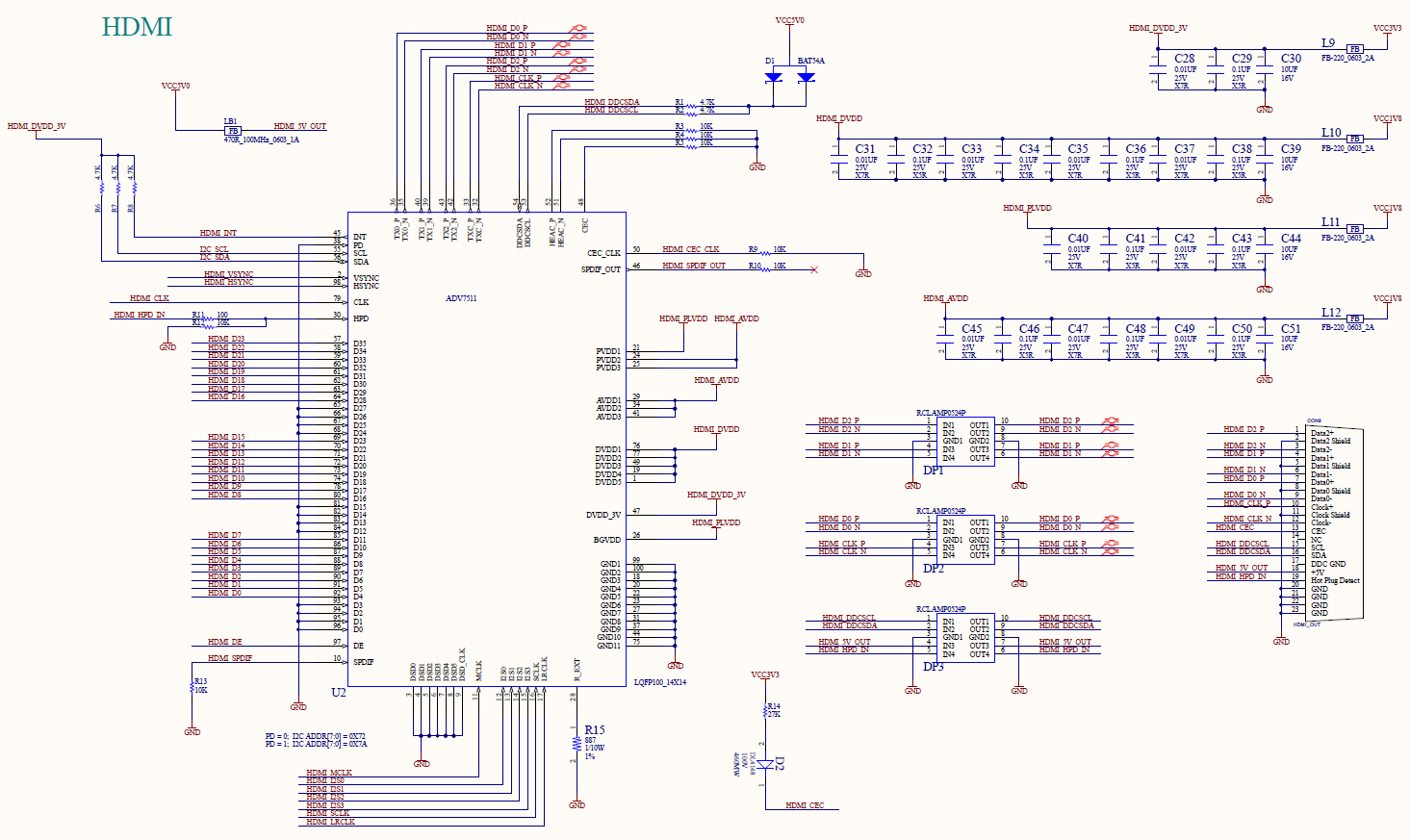
Figure 12.2 Schematics of HDMI
ADV7511 chip is set through the IIC bus and send the picture information to be displayed to the chip through HDMI_D0 to HDMI_D23, and control signals HDMI_HSYNC and HDMI_VSYNC and the clock signal HDMI_CLK, which are transmitted to the PC through the HDMI interface after being processed internally by the chip.
13.3.3 Program Introduction
The configuration part of the ADV7511 chip is carried out using the IIC protocol, with reference to Experiment 11 and Experiment 12. A brief introduction to the data processing section is now available.
| module hdmi_test (
input inclk_p, input inclk_n, input rst, input key1, output rgb_hs, output rgb_vs, output [7:0] rgb_r, output [7:0] rgb_g, output [7:0] rgb_b, output rgb_clk, inout scl, inout sda, output en ); endmodule |
FPGA configures the ADV7511 chip through the IIC bus (clock line scl, data line sda). After the configuration is complete, the output image information needs to be determined. Taking the 1080P (1920 * 1080) image format as an example, the data signals rgb_r (red component), rgb_g (green component), rgb_b (blue component), line synchronization signal rgb_hs, field synchronization signal rgb_vs, and a clock rgb_clk will be output. Each pixel is formed by a combination of three color components. Each row of 1920 pixels is filled with color information in a certain order (from left to right). After one line is completed, the next line is completed in a certain order (from top to bottom) until 1080 lines have been finihsed, so one frame of image information is completed. The image information of each frame is determined by this horizontal and vertical scanning, and then transmitted to the ADV7511 for processing. The timing diagrams of horizontal and vertical scanning are shown in Figures 12.3 and 12.4.
Figure 12.3 Horizontal synchronization
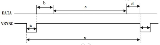
Figure 12.4 Vertical synchronization
The second step: data definition of 1080p image timing generation
| Horizontal line scan parameter setting 1920*1080@60 Hz clock 130 MHz
parameter LinePeriod = 2000; //Line period parameter H_SyncPulse = 12; //Line sync pulse (Sync a) parameter H_BackPorch = 40; //Display back edge (Back porch b) parameter H_ActivePix = 1920; // Display timing (Display interval c) parameter H_FrontPorch= 28; //Display front edge (Front porch d) parameter Hde_start = 52; parameter Hde_end = 1972; Vertical scan parameter setting 1920*1080@60Hz parameter FramePeriod = 1105; //Frame period parameter V_SyncPulse = 4; //Vertical sync pulse (Sync o) parameter V_BackPorch = 18; //Display trailing edge (Back porch p) parameter V_ActivePix = 1080; //Display timing (Display interval q) parameter V_FrontPorch= 3; //Display front edge (Front porch r) parameter Vde_start = 22; parameter Vde_end = 1102;
reg [12:0] x_cnt; reg [10:0] y_cnt; reg [23:0] grid_data_1; reg [23:0] grid_data_2; reg [23:0] bar_data; reg [3:0] rgb_dis_mode; reg [7:0 ] rgb_r_reg; reg [7:0] rgb_g_reg; reg [7:0] rgb_b_reg; reg hsync_r; reg vsync_r; reg hsync_de; reg vsync_de; reg [15:0] key1_counter; //pushu button
wire locked; reg rst; wire [12:0] bar_interval;
assign bar_interval = H_ActivePix[15: 3]; //Color strip width |
The third step: generate display content
| always @ (posedge rgb_clk)
begin if (rst) hsync_r <= 1’b1; else if (x_cnt == LinePeriod) hsync_r <= 1’b0; else if (x_cnt == H_SyncPulse) hsync_r <= 1’b1; if (rst) hsync_de <= 1’b0; else if (x_cnt == Hde_start) hsync_de <= 1’b1; else if (x_cnt == Hde_end) hsync_de <= 1’b0; end always @ (posedge rgb_clk) begin if (rst) y_cnt <= 1’b1; else if (x_cnt == LinePeriod) begin if (y_cnt == FramePeriod) y_cnt <= 1’b1; else y_cnt <= y_cnt + 1’b1; end end always @ (posedge rgb_clk) begin if (rst) vsync_r <= 1’b1; else if ((y_cnt == FramePeriod) &(x_cnt == LinePeriod)) vsync_r <= 1’b0; else if ((y_cnt == V_SyncPulse) &(x_cnt == LinePeriod)) vsync_r <= 1’b1; if (rst) vsync_de <= 1’b0; else if ((y_cnt == Vde_start) & (x_cnt == LinePeriod)) vsync_de <= 1’b1; else if ((y_cnt == Vde_end) & (x_cnt == LinePeriod)) vsync_de <= 1’b0; end assign en = hsync_de & vsync_de; always @(posedge rgb_clk) begin if ((x_cnt[4]==1’b1) ^ (y_cnt[4]==1’b1)) grid_data_1 <= 24’h000000; else grid_data_1<= 24’hffffff; if ((x_cnt[6] == 1’b1) ^ (y_cnt[6] == 1’b1)) grid_data_2 <=24’h000000; else grid_data_2 <=24’hffffff; end always @ (posedge rgb _clk) begin if (x_cnt==Hde_start) bar_data <= 24’hff0000; //Red strip else if (x_cnt == Hde_start + bar_interval) bar_data <= 24’h00ff00; //Green strip else if (x_cnt == Hde_start + bar_interval*2) bar_data <= 24’h0000ff; //Blue strip else if (x_cnt == Hde_start + bar_interval*3) bar_data <= 24’hff00ff; //Purple strip else if (x_cnt == Hde_start + bar_interval*4) bar_data <= 24’hffff00; //Yellow strip else if (x_cnt == Hde_start + bar_interval*5) bar_data <= 24’h00ffff; //Light blue strip else if (x_cnt == Hde_start + bar_interval*6) bar_data <= 24’hffffff; //White strip else if (x_cnt == Hde_start + bar_interval*7) bar_data <= 24’hff8000; //Orange strip else if (x_cnt == Hde_start + bar_interval*8) bar_data <= 24’h000000; //Black strip end always @ (posedge rgb_clk) begin if (rst) begin rgb_r_reg <= 0; rgb_g_reg <= 0; rgb_b_reg <= 0; end else case (rgb_dis_mode) 4’b0000 : //Display all black begin rgb_r_reg <= 0; rgb_g_reg <= 0; rgb_b_reg <= 0; end 4’b0001 : //Display all white begin rgb_r_reg <= 8’hff; rgb_g_reg <= 8’hff; rgb_b_reg <= 8’hff; end 4’b0010 : //Display all red begin rgb_r_reg <= 8’hff; rgb_g_reg <= 0; rgb_b_reg <= 0; end 4’b0011 : //Display all green begin rgb_r_reg <= 0; rgb_g_reg <= 8’hff; rgb_b_reg <= 0; end 4’b0100 : //Display all blue begin rgb_r_reg <= 0; rgb_g_reg <= 0; rgb_b_reg <= 8’hff; end 4’b0101 : // Display square 1 begin rgb_r_reg <= grid_data_1[23:16]; rgb_g_reg <= grid_data_1[15:8]; rgb_b_reg <= grid_data_1[7:0]; end 4’b0110 : // Display square 2 begin rgb_r_reg <= grid_data_2[23:16]; rgb_g_reg <= grid_data_2[15:8]; rgb_b_reg <= grid_data_2[7:0]; end 4’b0111 : // Display horizontal gradient begin rgb_r_reg <= x_cnt[10:3]; rgb_g_reg <= x_cnt[10:3]; rgb_b_reg <= x_cnt[10:3]; end 4’b1000 : // Display vertical gradient begin rgb_r_reg <= y_cnt[10:3]; rgb_g_reg <= y_cnt[10:3]; rgb_b_reg <= y_cnt[10:3]; end 4’b1001 : // Display red horizontal gradient begin rgb_r_reg <= x_cnt[10:3]; rgb_g_reg <= 0; rgb_b_reg <= 0; end 4’b1010 : // Display green horizontal gradient begin rgb_r_reg <= 0; rgb_g_reg <= x_cnt[10:3]; rgb_b_reg <= 0; end 4’b1011 : // Display blue horizontal gradient begin rgb_r_reg <= 0; rgb_g_reg <= 0; rgb_b_reg <= x_cnt[10:3]; end 4’b1100 : // Display colorful strips begin rgb_r_reg <= bar_data[23:16]; rgb_g_reg <= bar_data[15:8]; rgb_b_reg <= bar_data[7:0]; end default : // Display all white begin rgb_r_reg <= 8’hff; rgb_g_reg <= 8’hff; rgb_b_reg <= 8’hff; end endcase end assign rgb_hs = hsync_r; assign rgb_vs = vsync_r; assign rgb_r = (hsync_de & vsync_de) ? rgb_r_reg : 8’h00; assign rgb_g = (hsync_de & vsync_de) ? rgb_g_reg : 8’b00; assign rgb_b = (hsync_de & vsync_de) ? rgb_b_reg : 8’h00;
always @(posedge rgb_clk) begin if (key1 == 1’b1) key1_counter <= 0; else if ((key1 == 1’b0) & (key1_counter <= 16’d130000)) key1_counter <= key1_counter + 1’b1; if (key1_counter == 16’h129999) begin if(rgb_dis_mode == 4’b1100) rgb_dis_mode <= 4’b0000; else rgb_dis_mode <= rgb_dis_mode + 1’b1; end end |
When the push button is pressed, a key1 signal will be input, and the content displayed on the screen will change according to the change of vga_dis_mode, and the corresponding picture content will be displayed.
13.4 Experiment Verification
The first step: assign the pins
The pin assignment is shown in Table 12.1.
Table 12.1 HDMI experiment pin mapping table
| Signal Name | Network Name | FPGA Pin | Port Description |
| inclk_p | SYSCLK_P | AC13 | Input clock (differential)
200MHz |
| inclk_n | SYSCLK_N | AD13 | |
| rst | GPIO_SW_2 | F4 | Reset button |
| key1 | GPIO_SW_1 | G4 | Mode switching button |
| scl | IIC_SCL_MAIN_LS | W14 | IIC clock bus |
| sda | IIC_SDA_MAIN_LS | W17 | IIC data bus |
| rgb_clk | HDMI_R_CLK | AD19 | HDMI image clock |
| en | HDMI_R_DE | AE25 | HDMI image enable signal |
| rgb_hs | HDMI_R_HS | AA22 | Horizontal sync signal |
| rgb_vs | HDMI_R_VS | AE18 | Vertical sync signal |
| rgb_b[0] | HDMI_R_D0 | AD18 | Image blue output |
| rgb_b[1] | HDMI_R_D1 | AC18 | |
| rgb_b[2] | HDMI_R_D2 | AE26 | |
| rgb_b[3] | HDMI_R_D3 | AC21 | |
| rgb_b[4] | HDMI_R_D4 | AE23 | |
| rgb_b[5] | HDMI_R_D5 | AC22 | |
| rgb_b[6] | HDMI_R_D6 | AD25 | |
| rgb_b[7] | HDMI_R_D7 | AF19 | |
| rgb_g[0] | HDMI_R_D8 | AF24 | Image green output |
| rgb_g[1] | HDMI_R_D9 | AD26 | |
| rgb_g[2] | HDMI_R_D10 | AF20 | |
| rgb_g[3] | HDMI_R_D11 | AD23 | |
| rgb_g[4] | HDMI_R_D12 | AE20 | |
| rgb_g[5] | HDMI_R_D13 | AA23 | |
| rgb_g[6] | HDMI_R_D14 | AC19 | |
| rgb_g[7] | HDMI_R_D15 | AF25 | |
| rgb_r[0] | HDMI_R_D16 | AB19 | Image red output |
| rgb_r[1] | HDMI_R_D17 | AB24 | |
| rgb_r[2] | HDMI_R_D18 | AA19 | |
| rgb_r[3] | HDMI_R_D19 | AB21 | |
| rgb_r[4] | HDMI_R_D20 | AB20 | |
| rgb_r[5] | HDMI_R_D21 | AA24 | |
| rgb_r[6] | HDMI_R_D22 | W19 | |
| rgb_r[7] | HDMI_R_D23 | AB22 |
The second step: run the implementation, generate bitstream files, and verify the board
Download the generated programmable bitstream file to the Zynq_7030 development board. Press the switch button and the display content changes accordingly. The phenomenon is shown in the following figure. (List only a few)

Figure 12.5 HDMI display (all white)

Figure 12.6 HDMI display (square)

Figure 12.7 HDMI display (color strip)
Experiment 13 Ethernet
13.1 Experiment Objective
- Understand what Ethernet and how it works
- Familiar with the relationship between different interface types (MII, GMII, RGMII) and their advantages and disadvantages (here uses RGMII)
- Combine the development board to complete the transmission and reception of data and verify it
13.2 Experiment Implement
- Perform a loopback test to check if the hardware is working properly.
- Perform data receiving verification
- Perform data transmission verification
13.3 Experiment
13.3.1 Introduction to Experiment Principle
Ethernet is a baseband LAN technology. Ethernet communication is a communication method that uses coaxial cable as a network media and uses carrier multi-access and collision detection mechanisms. The data transmission rate reaches 1 Gbit/s, which can satisfy the need for data transfer of non-persistent networks. As an interconnected interface, the Ethernet interface is very widely used. There are many types of Gigabit Ethernet MII interfaces, and GMII and RGMII are commonly used.
MII interface has a total of 16 lines. See Figure 13. 1.
RXD(Receive Data)[3:0]: data reception signal, a total of 4 signal lines;
TX_ER(Transmit Error): send data error prompt signal, synchronized to TX_CLK, active high, indicating that the data transmitted during the valid period of TX_ER is invalid. For 10Mbps rate, TX_ER does not work;
RX_ER(Receive Error): receive data error prompt signal, synchronized to RX_CLK, active high, indicating that the data transmitted during the valid period of RX_ER is invalid. For 10 Mbps rate, RX_ER does not work;
TX_EN(Transmit Enable): send enable signal, only the data transmitted during the valid period of TX_EN is valid;
RX_DV(Reveive Data Valid): receive data valid signal, the action type is TX_EN of the transmission channel;
TX_CLK: transmit reference clock, the clock frequency is 25 MHz at 100 Mbps, and the clock frequency is 2.5 MHz at 10 Mbps. Note that the direction of TX_CLK clock is from the PHY side to the MAC side, so this clock is provided by the PHY;
RX_CLK: receive data reference clock, the clock frequency is 25 MHz at 100 Mbps, and the clock frequency is 2.5 MHz at 10 Mbps. RX_CLK is also provided by the PHY side;
CRS: carrier Sense, carrier detect signal, does not need to be synchronized to the reference clock. As long as there is data transmission, CRS is valid. In addition, CRS is effective only if PHY is in half-duplex mode;
COL: collision detection signal, does not need to be synchronized to the reference clock, is valid only if PHY is in half-duplex mode.
GMII interface is shown in Figure 13. 2.
Compared with the MII interface, the data width of the GMII is changed from 4 bits to 8 bits. The control signals in the GMII interface such as TX_ER, TX_EN, RX_ER, RX_DV, CRS, and COL function are the same as those in the MII interface. The frequencies of transmitting reference clock GTX_CLK and the receiving reference clock RX_CLK are both 125 MHz (1000 Mbps / 8 = 125 MHz).
There is one point that needs special explanation here, that is, the transmitting reference clock GTX_CLK is different from the TX_CLK in the MII interface. The TX_CLK in the MII interface is provided by the PHY chip to the MAC chip, and the GTX_CLK in the GMII interface is provided to the PHY chip by the MAC chip. The directions are different.
In practical applications, most GMII interfaces are compatible with MII interfaces. Therefore, the general GMII interface has two transmitting reference clocks: TX_CLK and GTX_CLK (the directions of the two are different, as mentioned above). When used as the MII mode, TX_CLK and 4 of the 8 data lines are used.
See Figure 13.3 for RGMII interface.
RGMII, or reduced GMII, is a simplified version of GMII, which reduces the number of interface signal lines from 24 to 14 (COL/CRS port status indication signals are not shown here), the clock frequency is still 125 MHz, and the TX/RX data width is changed from 8 to 4 bits. To keep the transmission rate of 1000 Mbps unchanged, the RGMII interface samples data on both the rising and falling edges of the clock. TXD[3:0]/RXD[3:0] in the GMII interface is transmitted on the rising edge of the reference clock, and TXD[7:4]/RXD[7:4] in the GMII interface is transmitted on the falling edge of the reference clock. RGMI is also compatible with both 100 Mbps and 10 Mbps rates, with reference clock rates of 25 MHz and 2.5 MHz, respectively.
The TX_EN signal line transmits TX_EN and TX_ER information, TX_EN is transmitted on the rising edge of TX_CLK, and TX_ER is transmitted on the falling edge. Similarly, RX_DV and RX_ER are transmitted on the RX_DV signal line, and RX_DV is transmitted on the rising edge of RX_CLK, and RX_ER is transmitted on the falling edge.
14.3.2 Hardware Design
Figure 13.4 Schematics of 88E1512
A 88E1512 chip is used on the experimental board to form a Gigabit Ethernet module. The schematics is shown in Figure 13.4. The PHY chip is connected to the FPGA by receiving and transmitting two sets of signals. The receiving group signal prefix is PL_PHY_RX, and the transmitting group signal prefix is PL_PHY_TX, which are respectively composed of a control signal CTL, a clock signal CK and four data signals 3-0. PL_PHY_ LED0 and PL_PHY_LED1 are respectively connected to the yellow signal light and the green signal light of the network port. At the same time, the FPGA can configure the PHY chip through the clock line NPHY_MDC and the data line NPHY_MDIO.
14.3.3 Program Introduction
- Configure IP address
Before verification (the default PC NIC is a Gigabit NIC, otherwise it needs to be replaced). PC IP address needs to be confirmed first. In the DOS command window, type ipconfig -all command to check it. Example is shown in Figure 13. 5.
Figure 13.5 PC end IP information
To facilitate subsequent experiments, PC is provided a fixed IP address. Take this experiment as an example, IP configuration is 192.169.0.100(could be revised, but needs to be consistent to the IP address of target sending module, for Internet Protocol reason, IP address 169.XXX.X.X is not suggested). Find Internet Protocol Version 4(TCP/IPv4) in Network and Sharing center. See Fig 13. 6.
Figure 13.6 Configure PC end IP address
Since there is no ARP protocol content (binding IP address and MAC address of the develop board) in this experiment, it needs to be bound manually through the DOS command window. Here, the IP is set to 192.168.0.2 and the MAC address is set to 00-0A-35-01-FE-C0, (can be replaced) as shown in Figure 13. 7, the method is as follows: (Note: Run the DOS command window as an administrator)
Run the command: ARP -s 192.168.0.2 00-0A-35-01-FE-C0
View binding results: ARP -a
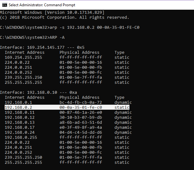
Figure 13.7 Address binding method 1
If a failure occurs while running the ARP command, another way is available, as shown in Figure 13.8:
- Enter the netsh i i show in command to view the number of the local connection, such as the “23” of the computer used this time.
- Enter netsh -c “i i” add neighbors 23 (number) “192.168.0.2” “00-0A-35-01-FE-C0”
- Enter arp -a to view the binding result
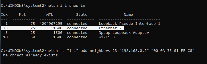
Figure 13.8 Address binding method 2
Next, the DOS command window is also used for connectivity detection, as shown in Figure 13. 9. Ping is an executable command that comes with the Windows family. Use it to check if the network can be connected. It can help analyze and determine network faults. Application format: Ping IP address (not host computer IP).
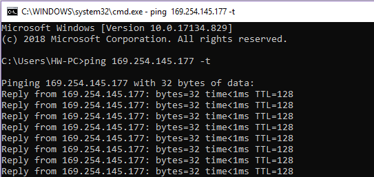
Figure 13.9 Send data
- Loopback test
The first step: program introduction
The loopback test only needs to output the input data directly. Refer the project file “loopback”. In the project, two IP cores, IDDR and ODDR, are used to complete the receiving and transmitting functions.
| module loopback(
input rst, input rxc, input rxdv, input [3:0] rxd, output txc, output txen, output [3:0] txd ); wire pll_locked; wire rx_clk; wire clk_125m, clk_125m_90; wire [7:0] e_rxd; wire rxdv1, rxdv2; clk_wiz_0 clk_wiz_0_inst( .clk_in1 (rx_clk), .reset (1’b0), .locked (pll_locked), .clk_out1 (clk_125m), .clk_out2 (clk_125m_90) ); ddio_in ddio_in_inst ( .data_in_from_pins ({rxdv, rxd}), .data_in_to_device ({rxdv2, e_rxd[7:4], rxdv1, e_rxd[3:0]}), .clk_in (rxc), .clk_out (rx_clk), .io_reset (1’b0) ); ddio_out ddio_out_inst ( .data_out_from_device ({rxdv2, e_rxd[7:4], rxdv1, e_rxd[3:0]}), .data_out_to_pins ({txen, txd}), .clk_in (clk_125m_90), .clk_out (txc), .io_reset (1’b0) ); endmodule |
Because it is the RGMII interface, the data is bilateral along 4-bit data. Therefore, when data processing is performed inside the FPGA, it needs to be converted into 8-bit data. Go to Installed IP > Library > Basic Functions > I/O to find ALTDDIO_IN and ALTDDIO_OUT. To implement it, IP core (ddio_in) is called, and after internal data processing, IP core is passed (ddio_out) to convert 8-bit data into bilateral edge 4-bit data transfer. It should be noted that, considering the enable signal and data signal synchronization, the enable signal is entered to ddio for conversion at the same time. The specific settings are shown in Figure 13. 10 and Figure 13. 11.
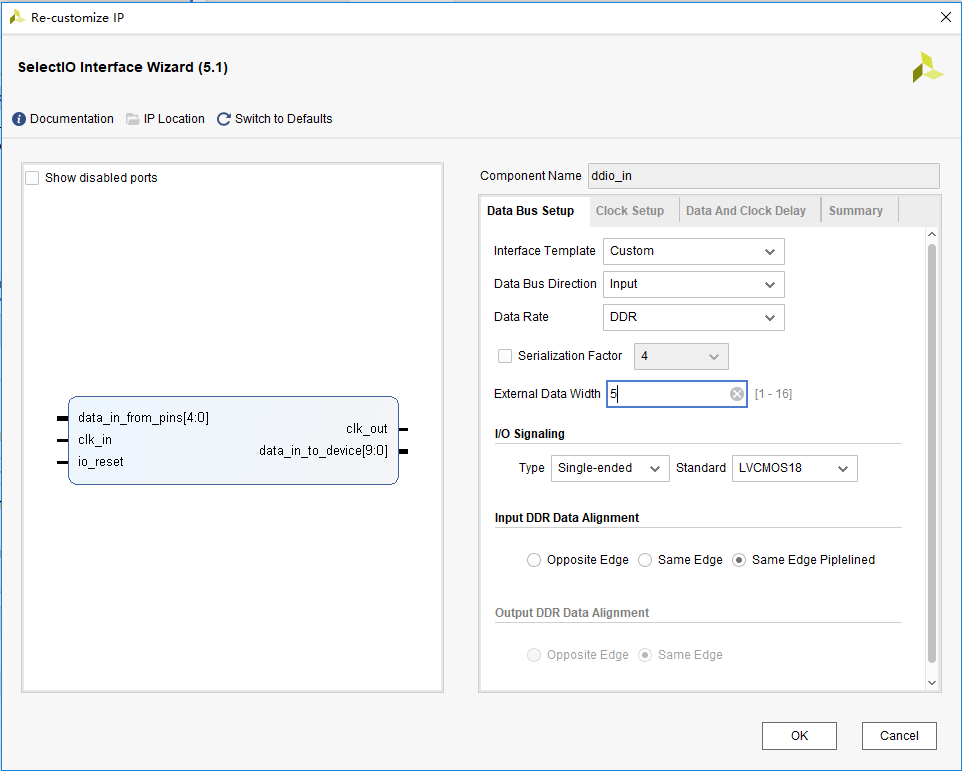
Figure 13.10 ddio_in setting
Figure 13.11 ddio_out setting
The secons step: assign pins, run implementation, verify the board
See Table 13.1 for the pin assignment.
Table 13.1 Ethernet experiment pin mapping table
| Signal Name | Network Name | FPGA Pin | Port Description |
| rst | GPIO_SW_2 | F4 | Reset |
| rxc | PL_PHY_RX_CLK | J4 | Receive clock |
| rxdv | PL_PHY_RX_CTRL | L3 | Receive enable clock |
| rxd[0] | PL_PHY_RXD[0] | K3 | Receive data (4-bit bilateral) |
| rxd[1] | PL_PHY_RXD[1] | K1 | |
| rxd[2] | PL_PHY_RXD[2] | H2 | |
| rxd[3] | PL_PHY_RXD[3] | G1 | |
| txc | PL_PHY_TX_CLK | N3 | Transmit clock |
| txen | PL_PHY_TX_CTRL | K5 | Transmit enable clock |
| txd[0] | PL_PHY_TXD[0] | M2 | Transmit data (4-bit bilateral) |
| txd[1] | PL_PHY_TXD[1] | L2 | |
| txd[2] | PL_PHY_TXD[2] | L4 | |
| txd[3] | PL_PHY_TXD[3] | L5 |
As shown in Figure 13.12, after setting the correct address and data type, the detection information (love you!) is sent through the host computer. The data packet is captured by Wireshark, as shown in Figure 13.13. The data is correctly transmitted back to the PC.
Figure 13.12 Host computer transmits the test data
Figure 13.13 PC end receives data correctly
- Complete Ethernet data transmission design
For complete Ethernet data transmission, it is necessary to have the receiving part of the data and the transmitting part of the data. For the convenience of experiment, the data transmitted by the PC is stored first in the RAM. After reading via the transmitting end, send it to the PC. For a series of data unpacking and packaging during the process, refer to the project file “ethernet”. A brief introduction to each module follows.
- Data receiving module (ip_receive)
This module is to detect and identify the data frame, unpack the valid data frame, and store the real data in the RAM.
| always @ (posedge clk) begin
if (clr) begin rx_state <= idle; data_receive <= 1’b0; end else case (rx_state)
idle : begin valid_ip_P <= 1’b0; byte_counter <= 3’d0; data_counter <= 10’d0; mydata <= 32’d0; state_counter <= 5’d0; data_o_valid <= 1’b0; ram_wr_addr <= 0; if (e_rxdv == 1’b1) begin if (datain[7:0] == 8’h55) begin //Receive the first 55// rx_state <= six_55; mydata <= {mydata[23:0], datain[7:0]}; end else rx_state <= idle; end end
six_55 : begin //Receive 6 0x55// if ((datain[7:0] == 8’h55) && (e_rxdv == 1’b1)) begin if (state_counter == 5) begin state_counter <= 0; rx_state <= spd_d5; end else state_counter <= state_counter + 1’b1; end else rx_state <= idle; end
spd_d5 : begin //Receive one 0xd5// if ((datain[7:0] == 8’hd5) && (e_rxdv == 1’b1)) rx_state <= rx_mac; else rx_state <= idle; end
rx_mac : begin //Receive target MAC address and source MAC address if (e_rxdv == 1’b1) begin if (state_counter < 5’d11) begin mymac <= {mymac[87:0], datain}; state_counter <= state_counter + 1’b1; end else begin board_mac <= mymac[87:40]; pc_mac <= {mymac[39:0], datain}; state_counter <= 5’d0; if ((mymac[87:72] == 16’h000a) && (mymac[71:56] == 16’h3501) && (mymac[55:40] == 16’hfec0)) //Determine if the target MAC Address is from the current FPGA rx_state <= rx_IP_Protocol; else rx_state <= idle; end end else rx_state <= idle; end
rx_IP_Protocol : begin //Receive 2 bytes of IP TYPE if (e_rxdv == 1’b1) begin if (state_counter < 5’d1) begin myIP_Prtcl <= {myIP_Prtcl[7:0], datain[7:0]}; state_counter <= state_counter+1’b1; end else begin IP_Prtcl <= {myIP_Prtcl[7:0],datain[7:0]}; valid_ip_P <= 1’b1; state_counter <= 5’d0; rx_state <= rx_IP_layer; end end else rx_state <= idle; end
rx_IP_layer : begin //Receive 20 bytes of udp virtual header, ip address valid_ip_P <= 1’b0; if (e_rxdv == 1’b1) begin if (state_counter < 5’d19) begin myIP_layer <= {myIP_layer[151:0], datain[7:0]}; state_counter <= state_counter + 1’b1; end else begin IP_layer <= {myIP_layer[151:0], datain[7:0]}; state_counter <= 5’d0; rx_state <= rx_UDP_layer; end end else rx_state <= idle; end
rx_UDP_layer : begin // Receive 8-byte UDP port number and UDP packet length rx_total_length <= IP_layer[143:128]; pc_IP <= IP_layer[63:32]; board_IP <= IP_layer[31:0]; if (e_rxdv == 1’b1) begin if (state_counter < 5’d7) begin myUDP_layer <= {myUDP_layer[55:0], datain[7:0]}; state_counter <= state_counter + 1’b1; end else begin UDP_layer <= {myUDP_layer[55:0], datain[7:0]}; rx_data_length <= myUDP_layer[23:8]; //length of UDP data package state_counter <= 5’d0; rx_state <= rx_data; end end else rx_state <= idle; end
rx_data : begin //Receive UDP data if (e_rxdv == 1’b1) begin if (data_counter == rx_data_length-9) begin //Save last data data_counter <= 0; rx_state <= rx_finish; ram_wr_addr <= ram_wr_addr + 1’b1; data_o_valid <= 1’b1; // Write RAM if (byte_counter == 3’d3) begin data_o <= {mydata[23:0], datain[7:0]}; byte_counter <= 0; end else if (byte_counter==3’d2) begin data_o <= {mydata[15:0], datain[7:0],8’h00}; //Less than 32-bit, //add ‘0’ byte_counter <= 0; end else if (byte_counter==3’d1) begin data_o <= {mydata[7:0], datain[7:0], 16’h0000}; //Less than //32-bit , add ‘0’ byte_counter <= 0; end else if (byte_counter==3’d0) begin data_o <= {datain[7:0], 24’h000000}; //Less than 32-bit, //add ‘0’ byte_counter <= 0; end end else begin data_counter <= data_counter + 1’b1; if (byte_counter < 3’d3) begin mydata <= {mydata[23:0], datain[7:0]}; byte_counter <= byte_counter + 1’b1; data_o_valid <= 1’b0; end else begin data_o <= {mydata[23:0], datain[7:0]}; byte_counter <= 3’d0; data_o_valid <= 1’b1; // Receive 4bytes of data, write //RAM request ram_wr_addr <= ram_wr_addr+1’b1; end end end else rx_state <= idle; end
rx_finish : begin data_o_valid <= 1’b0; //added for receive test// data_receive <= 1’b1; rx_state <= idle; end default : rx_state <= idle; endcase end |
The receiving module is to perform step by step analysis on the received data.
Idle state: If ‘55’ is received, jump to the six_55 state.
Six_55 state: If it continues to receive six consecutive 55s, it will jump to the spd_d5 state, otherwise it will return the idle state.
Spd_d5 state: If ‘d5’ continues received, it proves that the complete packet preamble “55_55_55_55_55_55_55_d5” has been received, and jumps to rx_mac, otherwise it returns the idle transition.
rx_mac state: This part is the judgment of the target MAC address and the source MAC address. If it matches, jump to the rx_IP_Protocol state, otherwise it will return the idle state and resend.
rx_IP_Protocol state: Determine the type and length of the packet and jump to the rx_IP_layer state.
rx_IP_layer state: Receive 20 bytes of UDP virtual header and IP address, jump to rx_UDP_layer state
rx_UDP_layer state: Receive 8-byte UDP port number and UDP packet length, jump to rx_data state
Rx_data state: Receive UDP data, jump to rx_finish state
Rx_finish state: A packet of data is received, and jump to the idle state to wait for the arrival of the next packet of data.
- Data sending module (ip_send)
The main content of this module is to read out the data in the RAM, package and transmit the data with the correct packet protocol type (UDP). Before transmitting, the data is also checked by CRC.
| initial begin
tx_state <= idle; //Define IP header preamble[0] <= 8’h55; //7 preambles “55”, one frame start //character “d5” preamble[1] <= 8’h55; preamble[2] <= 8’h55; preamble[3] <= 8’h55; preamble[4] <= 8’h55; preamble[5] <= 8’h55; preamble[6] <= 8’h55; preamble[7] <= 8’hD5;
mac_addr[0] <= 8’hB4; //Target MAC address “ff-ff-ff-ff-ff-ff”, full ff is //broadcast package mac_addr[1] <= 8’h2E; //Target MAC address “B4-2E-99-20-C4-61”, // For the PC-side address used for this experiment, change the content according to the actual //PC in the debugging phase. mac_addr[2] <= 8’h99; mac_addr[3] <= 8’h20; mac_addr[4] <= 8’hC4; mac_addr[5] <= 8’h61;
mac_addr[6] <= 8’h00; //Source MAC address “00-0A-35-01-FE-C0” mac_addr[7] <= 8’h0A; //Modify it according to the actual needs mac_addr[8] <= 8’h35; mac_addr[9] <= 8’h01; mac_addr[10]<= 8’hFE; mac_addr[11]<= 8’hC0;
mac_addr[12]<= 8’h08; //0800: IP package type mac_addr[13]<= 8’h00;
i<=0; end |
This part defines the preamble of the data packet, the MAC address of the PC, the MAC address of the development board, and the IP packet type. It should be noted that in the actual experiment, the MAC address of the PC needs to be modified. Keep the MAC address consistent along the project, otherwise the subsequent experiments will not receive data.
| always @ (posedge clk) begin
case (tx_state) idle : begin e_txen <= 1’b0; crcen <= 1’b0; crcre <= 1; j <= 0; dataout <= 0; ram_rd_addr <= 1; tx_data_counter <= 0; if (time_counter == 32’h04000000) begin //Wait for the delay, send a data //package regularly tx_state <= start; time_counter <= 0; end else time_counter <= time_counter + 1’b1; end
start : begin //IP header ip_header[0] <= {16’h4500, tx_total_length}; //Version: 4; IP header length: 20; //IP total length ip_header[1][31:16] <= ip_header[1][31:16]+1’b1; // Package serial number ip_header[1][15:0] <= 16’h4000; //Fragment offset ip_header[2] <= 32’h80110000; //mema[2][15:0] protocol: 17(UDP) ip_header[3] <= 32’hc0a80002; //Source MAC address ip_header[4] <= 32’hc0a80003; //Target MAC address ip_header[5] <= 32’h1f901f90; // 2-byte source port number and //2-byte target port number ip_header[6] <= {tx_data_length, 16’h0000}; //2 bytes of data length and 2 //bytes of checksum (none) tx_state <= make; end
make : begin // Generate a checksum of the header if (i == 0) begin check_buffer <= ip_header[0][15:0] + ip_header[0][31:16] + ip_header[1][15:0] + ip_header[1][31:16] + ip_header[2][15:0] + ip_header[2][31:16] + ip_header[3][15:0] + ip_header[3][31:16] + ip_header[4][15:0] + ip_header[4][31:16]; i <= i + 1’b1; end else if(i == 1) begin check_buffer[15:0] <= check_buffer[31:16] + check_buffer[15:0]; i <= i+1’b1; end else begin ip_header[2][15:0] <= ~check_buffer[15:0]; //header checksum i <= 0; tx_state <= send55; end end
send55 : begin // Send 8 IP preambles: 7 “55”, 1 “d5” e_txen <= 1’b1; //GMII transmitted valid data crcre <= 1’b1; //reset crc if(i == 7) begin dataout[7:0] <= preamble[i][7:0]; i <= 0; tx_state <= sendmac; end else begin dataout[7:0] <= preamble[i][7:0]; i <= i + 1’b1; end end
sendmac : begin // Send target MAC address, source MAC address and IP packet type crcen <= 1’b1; // CRC check enable, crc32 data check starts from the target MAC crcre <= 1’b0; if (i == 13) begin dataout[7:0] <= mac_addr[i][7:0]; i <= 0; tx_state <= sendheader; end else begin dataout[7:0] <= mac_addr[i][7:0]; i <= i + 1’b1; end end
sendheader : begin // Send 7 32-bit IP headers datain_reg <= datain; //Prepare the data to be transmitted if(j == 6) begin if(i == 0) begin dataout[7:0] <= ip_header[j][31:24]; i <= i + 1’b1; end else if(i == 1) begin dataout[7:0] <= ip_header[j][23:16]; i <= i + 1’b1; end else if(i == 2) begin dataout[7:0] <= ip_header[j][15:8]; i <= i + 1’b1; end else if(i == 3) begin dataout[7:0] <= ip_header[j][7:0]; i <= 0; j <= 0; tx_state <= senddata; end end else begin if(i == 0) begin dataout[7:0] <= ip_header[j][31:24]; i <= i + 1’b1; end else if(i == 1) begin dataout[7:0] <= ip_header[j][23:16]; i <= i + 1’b1; end else if(i == 2) begin dataout[7:0] <= ip_header[j][15:8]; i <= i + 1’b1; end else if(i == 3) begin dataout[7:0] <= ip_header[j][7:0]; i <= 0; j <= j + 1’b1; end end end
senddata : begin //Transmit UDP packets if(tx_data_counter == tx_data_length – 9) begin //Transmit last data tx_state <= sendcrc; if (i == 0) begin dataout[7:0] <= datain_reg[31:24]; i <= 0; end else if (i == 1) begin dataout[7:0] <= datain_reg[23:16]; i <= 0; end else if (i == 2) begin dataout[7:0] <= datain_reg[15:8]; i <= 0; end else if (i == 3) begin dataout[7:0] <= datain_reg[7:0]; datain_reg <= datain; //Prepare the data i <= 0; end end else begin //Send other data package tx_data_counter <= tx_data_counter+1’b1; if (i == 0) begin dataout[7:0] <= datain_reg[31:24]; i <= i + 1’b1; ram_rd_addr <= ram_rd_addr + 1’b1; // Add 1 to the RAM address, //let the RAM output data in advance. end else if (i == 1) begin dataout[7:0] <= datain_reg[23:16]; i <= i + 1’b1; end else if (i == 2) begin dataout[7:0] <= datain_reg[15:8]; i <= i + 1’b1; end else if (i == 3) begin dataout[7:0] <= datain_reg[7:0]; datain_reg <= datain; //Prepare data i <= 0; end end end
sendcrc : begin //Send 32-bit CRC checksum crcen <= 1’b0; if (i == 0) begin dataout[7:0] <= {~crc[24], ~crc[25], ~crc[26], ~crc[27], ~crc[28], ~crc[29], ~crc[30], ~crc[31]}; i <= i + 1’b1; end else begin if (i == 1) begin dataout[7:0] <= {~crc[16], ~crc[17], ~crc[18], ~crc[19], ~crc[20], ~crc[21], ~crc[22], ~crc[23]}; i <= i + 1’b1; end else if (i == 2) begin dataout[7:0] <= {~crc[8], ~crc[9], ~crc[10], ~crc[11], ~crc[12], ~crc[13], ~crc[14], ~crc[15]}; i <= i + 1’b1; end else if (i == 3) begin dataout[7:0] <= {~crc[0], ~crc[1], ~crc[2], ~crc[3], ~crc[4], ~crc[5], ~crc[6], ~crc[7]}; i <= 0; tx_state <= idle; end end end
default : tx_state <= idle; endcase end |
Idle state: waiting for delay, sending a packet at regular intervals and jumping to the start state.
Start state: send the packet header and jump to the make state.
make state: generates the checksum of the header and jumps to the send55 state.
Send55 status: send 8 preambles and jump to the sendmac state.
sendmac state: send the target MAC address, source MAC address and IP packet type, and jump to the sendheader state.
sendheader state: sends 7 32-bit IP headers and jumps to the senddata state.
senddata state: send UDP packets and jump to the sendcrc state.
sendcrc state: sends 32-bit CRC check and returns the idle state.
Following the above procedure, the entire packet of data is transmitted, and the idle state is returned to wait for the transmission of the next packet of data.
- CRC check module (crc)
The CRC32 check of an IP packet is calculated at the destination MAC Address and until the last data of a packet. The CRC32 verilog algorithm and polynomial of Ethernet can be generated directly at the following website: http://www.easics.com/webtools/crctool
- UDP data test module (UDP)
This module only needs to instantiate the first three sub-modules together. Check the correctness of each connection.
- Top level module settings (ethernet)
The PLL, ddio_in, ddio_out, ram, and UDP modules are instantiated to the top level entity, and specific information is stored in advance in the RAM (Welcome To ZGZNXP World!). When there is no data input, the FPGA always sends this information. With data input, the received data is sent. Refer to the project files for more information.
13.4 Experiment Verification
The pin assignment of this test procedure is identical to that in loopback test.
Before programming the development board, it is necessary to note that the IP address of the PC and the MAC address of the development board must be determined and matched, otherwise the data will not be received.
Download the compiled project to the development board. As shown in Figure 13.14, the FPGA is keeping sending information to the PC. The entire transmitted packet can also be seen in Wireshark, as shown in Figure 13.15.
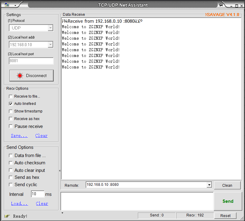
Figure 13.14 Send specific information
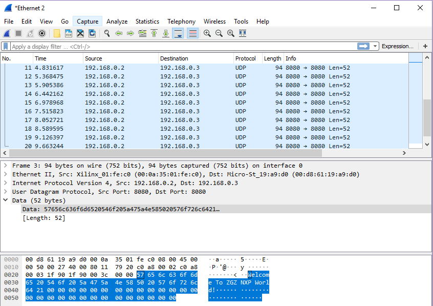
Figure 13.15 Specific information package
When the PC sends data to the FPGA, as shown in Figure 13.16, the entire packet arrives at the FPGA, and then the FPGA repackages the received data and sends it to the PC. See Figure 13.17, the network assistant also receives the transmitted data information accurately, as shown in Figure 13.18.

Figure 13.16 PC send data package
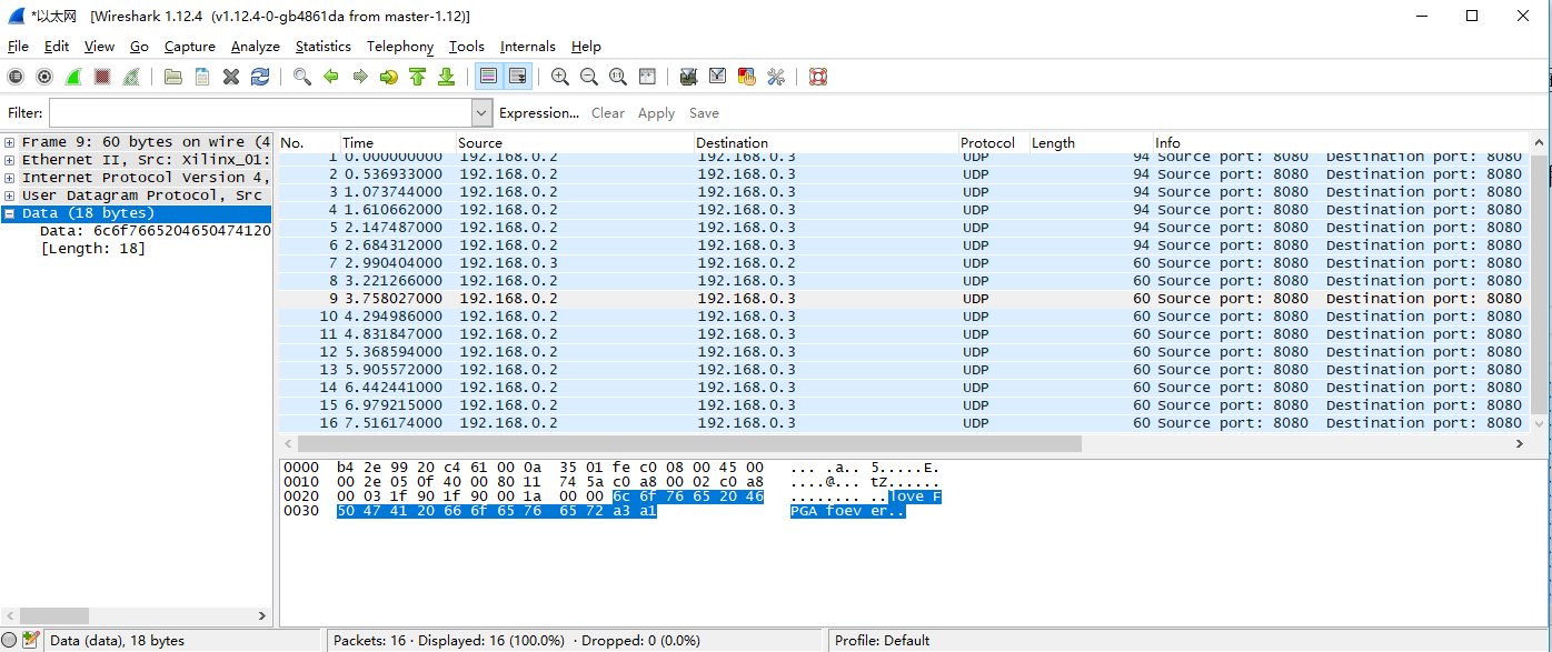
Figure 13.17 The FPGA repackages the received data and sends it to the PC
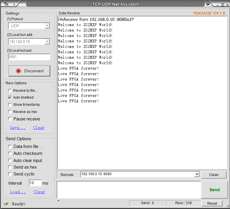
Figure 13.18 Information received by PC from FPGA
It should be noted that Ethernet II specifies the Ethernet frame data field is a minimum of 46 bytes, that is, the minimum Ethernet frame is 6+6+2+46+4=64. The 4-byte FCS is removed, so the packet capture is 60 bytes. When the length of the data field is less than 46 bytes, the MAC sublayer is padded after the data field to satisfy the data frame length of not less than 64 bytes. When communicating over a UDP LAN, “Hello World” often occurs for testing, but “Hello World” does not meet the minimum valid data (64-46) requirements. It is less than 18 bytes but the other party is still available for receiving, because data is complemented in the MAC sublayer of the link layer, less than 18 bytes are padded with ‘0’s. However, when the server is on the public network and the client is on the internal network, if less than 18 bytes of data is transmitted, the receiving end cannot receive the data. Therefore, if there is no data received, the information to be sent should be increased to more than 18 bytes.
References
-
- http://web.engr.oregonstate.edu/~traylor/ece474/beamer_lectures/verilog_operators.pdf
- https://www.utdallas.edu/~akshay.sridharan/index_files/Page5212.htm
- https://www.xilinx.com/support/documentation/sw_manuals/xilinx2015_2/ug908-vivado-programming-debugging.pdf
- https://www.xilinx.com/support/documentation/sw_manuals/xilinx2016_4/ug835-vivado-tcl-commands.pdf#nameddest=xwrite_cfgmem