interface types (MII, GMII, RGMII) advantages and disadvantages – Ethernet Experiment – FPGA Board for Beginner – Experiment 14
Experiment 14 Ethernet Experiment
14.1 Experiment Objective
- Understand what Ethernet is and how it works
- Familiar with the relationship between different interface types (MII, GMII, RGMII) and their advantages and disadvantages (our development board uses RGMII)
- Combine the development board to complete the transmission and reception of data and verify
14.2 Experiment Requirement
- Perform a loopback test to check if the hardware is working properly.
- Performing data verification
- Perform data transmission verification
14.3 Experiment
14.3.1 Experiment Principle
Ethernet is a baseband LAN technology. Ethernet communication is a communication method that uses coaxial cable as a network medium and uses carrier multi-access and collision detection mechanisms. The data transmission rate reaches 1 Gbit/s, which can satisfy the need for data transfer of non-persistent networks. As an interconnected interface, the Ethernet interface is very widely used. There are many types of Gigabit Ethernet MII interfaces, and GMII and RGMII are commonly used.
MII interface has a total of 16 lines. See Fig 14. 1.
RXD (Receive Data) [3:0]: data reception signal, a total of 4 signal lines;
TX_ER (Transmit Error): Send data error prompt signal, synchronized to TX_CLK, active high, indicating that the data transmitted during TX_ER validity period is invalid. For 10Mbps rate, TX_ER does not work;
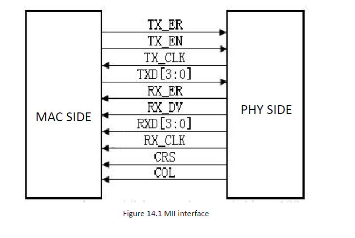 Fig 14. 1 MII interface
RX_ER (Receive Error): Receive data error prompt signal, synchronized to RX_CLK, active high, indicating that the data transmitted during the valid period of RX_ER is invalid. For 10Mbps, RX_ER does not work;
TX_EN (Transmit Enable): Send enable signal, only the data transmitted during the valid period of TX_EN is valid;
RX_DV (Receive Data Valid): Receive data valid signal, the action type is TX_EN of the transmission channel;
TX_CLK: Transmit reference clock, the clock frequency is 25MHz at 100Mbps, and the clock frequency is 2.5MHz at 10Mbps. Note that the direction of TX_CLK clock is from the PHY side to the MAC side, so this clock is provided by the PHY;
RX_CLK: Receive data reference clock, the clock frequency is 25MHz at 100Mbps, and the clock frequency is 2.5MHz at 10Mbps. RX_CLK is also provided by the PHY side;
CRS: Carrier Sense, carrier detect signal, does not need to synchronize with the reference clock. As long as there is data transmission, CRS is valid. In addition, CRS is effective only if PHY is in half-duplex mode;
COL: Collision detection signal, does not need to be synchronized to the reference clock, is valid only if PHY is in half-duplex mode.
GMII interface is shown in Fig 14. 2.
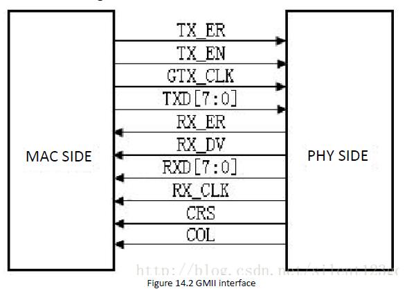
Figure 14. 2 GMII interface
Compared with the MII interface, the data width of the GMII is changed from 4 bits to 8 bits. The control signals in the GMII interface such as TX_ER, TX_EN, RX_ER, RX_DV, CRS, and COL function the same as those in the MII interface. The frequencies of transmitting reference clock GTX_CLK and the receiving reference clock RX_CLK are both 125 MHz (1000 Mbps / 8 = 125 MHz).
There is one point that needs special explanation here, that is, the transmitting reference clock GTX_CLK is different from the TX_CLK in the MII interface. The TX_CLK in the MII interface is provided by the PHY chip to the MAC chip, and the GTX_CLK in the GMII interface is provided to the PHY chip by the MAC chip. The directions are different.
In practical applications, most GMII interfaces are compatible with MII interfaces. Therefore, the general GMII interface has two transmitting reference clocks: TX_CLK and GTX_CLK (the directions of the two are different, as mentioned above). When used as the MII mode, TX_CLK and 4 of the 8 data lines are used.
See Fig 14. 3 for RGMII interface.
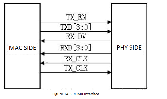
Fig 14. 3 RGMII Interface
RGMII, or reduced GMII, is a simplified version of GMII, which reduces the number of interface signal lines from 24 to 14 (COL/CRS port status indication signals, not shown here), the clock frequency is still 125MHz, and the TX/RX data width is changed from 8 to 4 bits. To keep the transmission rate of 1000 Mbps unchanged, the RGMII interface samples data on both the rising and falling edges of the clock. TXD[3:0]/RXD[3:0] in the GMII interface is transmitted on the rising edge of the reference clock, and TXD[7:4]/RXD[7:4] in the GMII interface is transmitted on the falling edge of the reference clock. RGMI is also compatible with both 100Mbps and 10Mbps rates, with reference clock rates of 25MHz and 2.5MHz, respectively.
The TX_EN signal line transmits TX_EN and TX_ER information, TX_EN is transmitted on the rising edge of TX_CLK, and TX_ER is transmitted on the falling edge. Similarly, RX_DV and RX_ER are transmitted on the RX_DV signal line, and RX_DV is transmitted on the rising edge of RX_CLK, and RX_ER is transmitted on the falling edge.
14.3.2 PCB Schematics
The development board uses the RTL8211E-VB chip to form a Gigabit Ethernet module. The schematic diagram of the PCB is shown in Fig 14. 4. 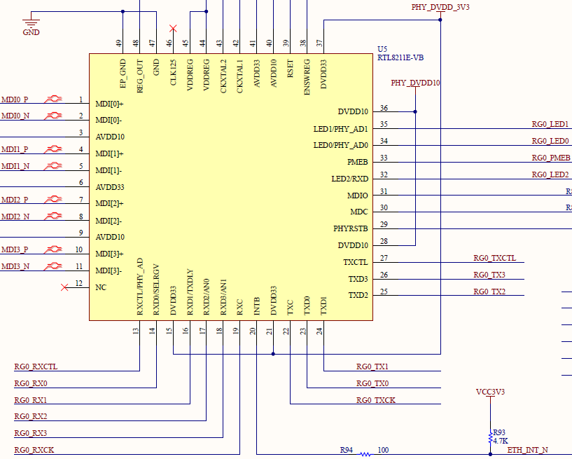
Fig 14. 4 RTL8211E-VB PCB schematics
14.3.3 Test Program Design
- Loopback test design (test1)
The loopback test is straightforward. Simply output the input data. Code is shown as below:
module test1 (rxc, rxdv, rxd, txc, txen, txd);
input rxc;
input rxdv;
input [3:0] rxd;
output txc;
output txen;
output [3:0] txd;
assign txd = rxd;
assign txen = rxdv;
assign txc = rxc;
endmodule
(Note: Each program in this experiment contains a smi_ctrl module. In the folder config, it is a setting module for the PHY chip, to solve the problem that some computers cannot connect to the network port normally, and will not explain in detail)
After compiling the code, lock the pins and downloading to the board. The pin assignments are shown in the table.
| Signal Name | Port Description | Network Label | FPGA Pin |
| rxc | Input clock | RG0_RXCK | 24 |
| rxdv | Input control signal | RG0_RXCTL | 34 |
| rxd[3] | Digit 3 of input data | RG0_RX3 | 28 |
| rxd[2] | Digit 2 of input data | RG0_RX2 | 31 |
| rxd[1] | Digit 1 of input data | RG0_RX1 | 32 |
| rxd[0] | Digit 0 of input data | RG0_RX0 | 33 |
| txc | Output clock | RG0_TXCK | 43 |
| txen | Output control signal | RG0_TXCTL | 42 |
| txd[3] | Digit 3 of output data | RG0_TX3 | 46 |
| txd[2] | Digit 2 of output data | RG0_TX2 | 49 |
| txd[1] | Digit 1 of output data | RG0_TX1 | 50 |
| txd[0] | Digit 0 of output data | RG0_TX0 | 51 |
| e_mdc | Configuration clock | NPHY_MDC | 38 |
| e_mdio | Configuration data | NPHY_MDIO | 39 |
Before verification (the default PC NIC is a Gigabit NIC, otherwise it needed to be replaced). You need to confirm your PC IP address first. In the DOS command window, type ipconfig -all command to check it. As an example, as shown in Fig 14. 5.
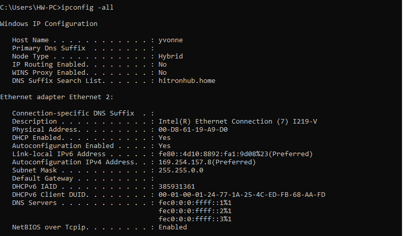
Fig 14. 5 PC end IP information
To facilitate subsequent experiments, provides PC a fixed IP address. Take this as an example, IP configuration is 169.254.157.8 (could be revised, but needs to be consistent to the IP address of target sending module). Find Internet Protocol Version 4(TCP/IPv4) in Network and Sharing center. See Fig 14. 6.
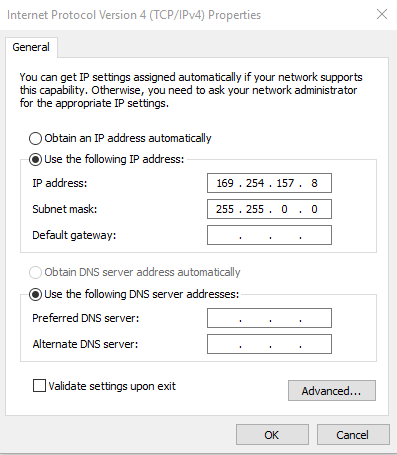
Fig 14. 6 Configure PC end IP address
Since there is no ARP protocol content (binding IP address and MAC address of the develop board) in this test, it needs to be bound manually through the DOS command window. In this test, the IP is set to 192.168.0.2 and the MAC address is set to 00-0A-35-01-FE-C0, (can be replaced by yourself) as shown in Fig 14. 7, the method is as follows: (Note: Run the DOS command window as an administrator)
Run the command: ARP -s 192.168.0.2 00-0A-35-01-FE-C0
View binding results: ARP -a
If a failure occurs while running the ARP command, you can bind it in another way, as shown in Fig 14. 7:
-
- Enter the netsh i i show in command to view the number of the local connection, such as the “23” of the computer used this time.
- Enter netsh -c “i i” add neighbors 23 (number) “192.168.0.2” “00-0A-35-01-FE-C0”
- Enter arp -a to view the binding result (since it has been bound before, it will display as shown below in Fig 14. 8)
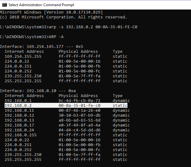
Fig 14. 7 Address binding method 1
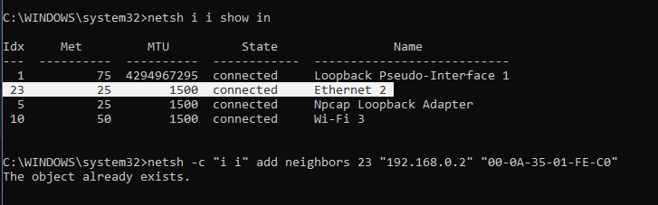
Fig 14. 8 Address binding method 2
Next, we also use the DOS command window for connectivity detection, as shown in Fig 14. 9. Ping is an executable command that comes with the Windows family. Use it to check if the network can be connected. It can help us analyze and determine network faults. Application format: Ping IP address (not host computer IP).
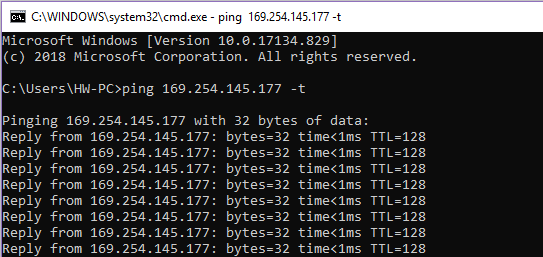
Fig 14. 9 Send data
Start SignalTap II, after sending the command, as shown in Fig 14. 10. The data is ordinary and the hardware is intact seen from the screenshot.
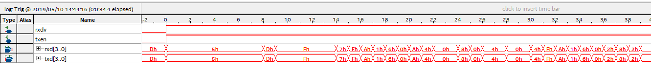
Fig 14. 10 SignalTap II data capture
- Special IP core configuration (test2)
Because it is the RGMII interface, the data is bilateral along 4-bit data. Therefore, when data processing is performed inside the FPGA, it needs to be converted into 8-bit data. Go to Installed IP > Library > Basic Functions > I/O to find ALTDDIO_IN and ALTDDIO_OUT. We call IP core (ddio_in) to implement it, and after internal data processing, pass IP core (ddio_out) to convert 8-bit data into double-rolled edge 4-bit data transfer. It should be noted that, considering the synchronization signal and data signal synchronization, the enable signal is entered to ddio for conversion. The specific settings are shown in Fig 14. 11 and Fig 14. 12.
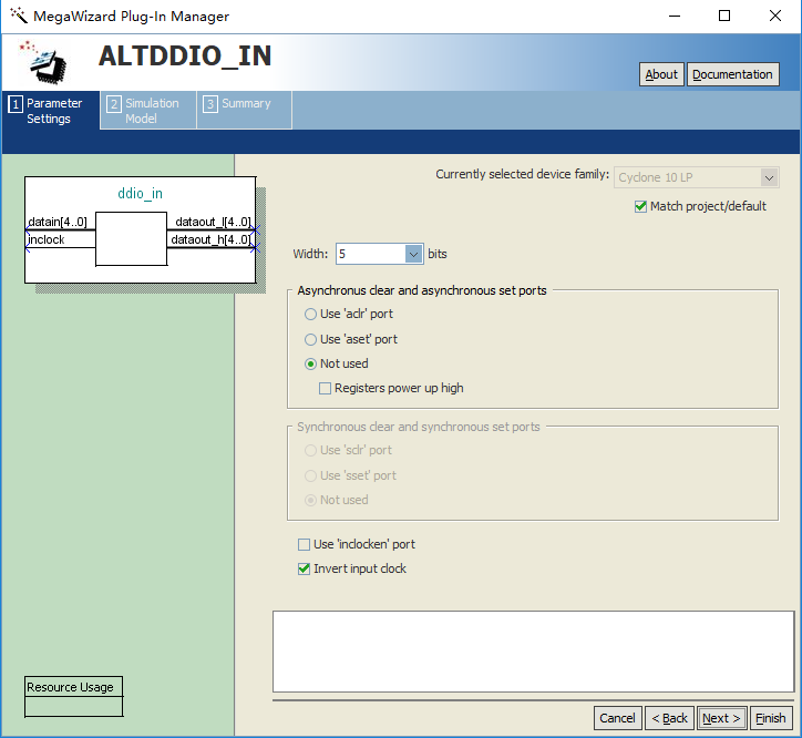
Fig 14. 11 ddio_in setting
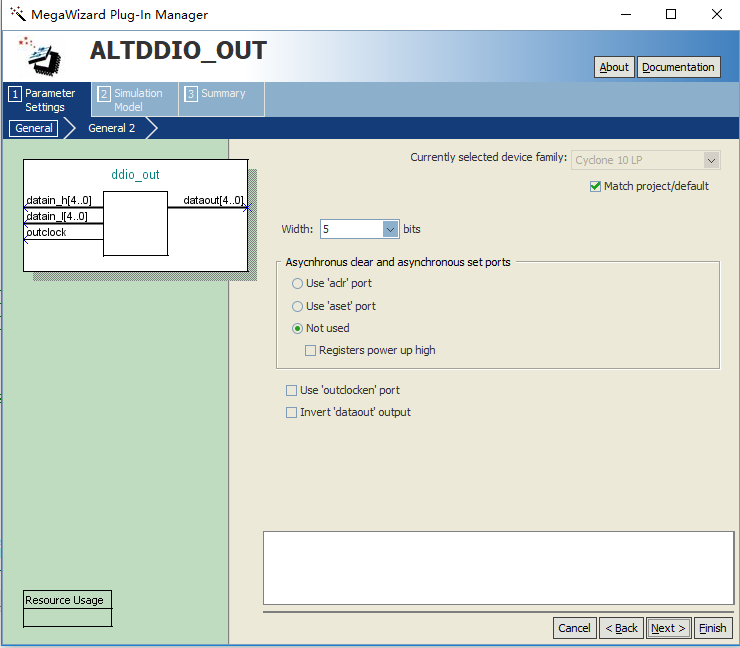
Fig 14. 12 ddio_out setting
Considering that the driving ability of the clock provided by the PHY chip is relatively poor, after the phase-locked loop processing, unlike the prior part, the input clock rxc selects the homologous input, as shown in Fig 14. 13, and outputs the C0 clock ddio_clk as two ddios. The driving clock of the IP core, as shown in Fig 14. 14, outputs the C1 clock txc as the data transmission clock (note that due to hardware circuit and timing reasons, txc needs to be 90° phase difference). See Fig 14. 15.
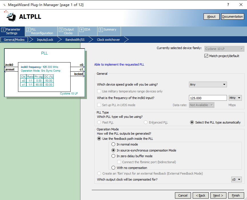
Fig 14. 13 PLL input clock setting
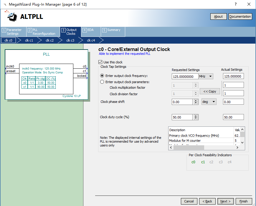
Fig 14. 14 PLL output clock (c0) setting
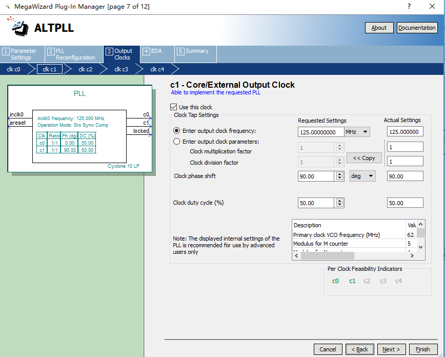
Fig 14. 15 PLL output clock (c1) setting
The three IP cores are instantiated into the previous loopback test, and the data transmission correctness test is performed. (It is necessary to notice the ordered timing. The ddio_out input data needs to be reversed. For details, refer to the project file (test2)). This time we used a network debugging assistant applet as an auxiliary testing tool. Download the program to the board and verify it.
As shown in Fig 14. 16, after setting the correct address and data type, we send the detection information (love you!) through the host computer. The data packet is captured by Wireshark, as shown in Fig 14. 17. The data is correctly transmitted back to the PC.
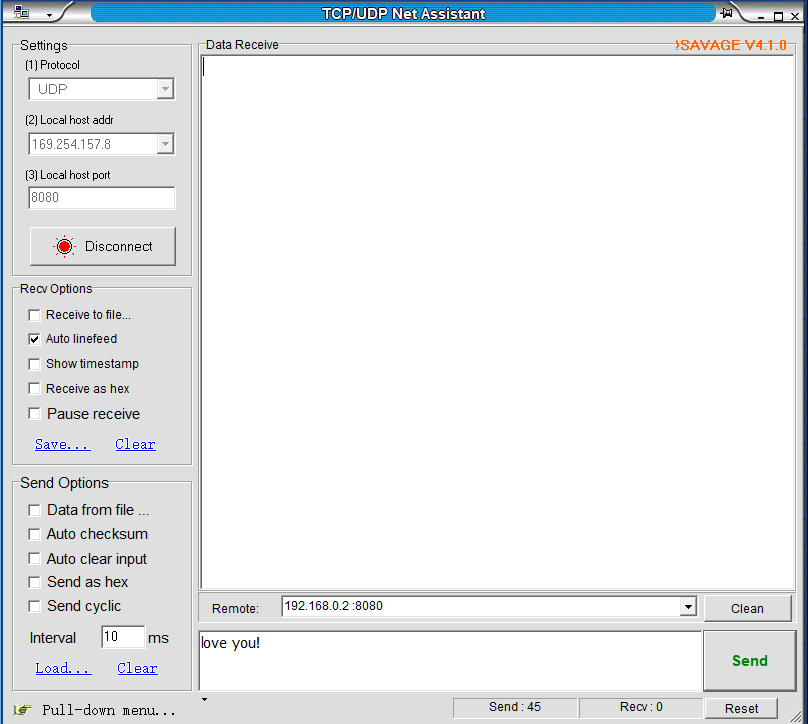
Fig 14. 16 The host computer sends the test data
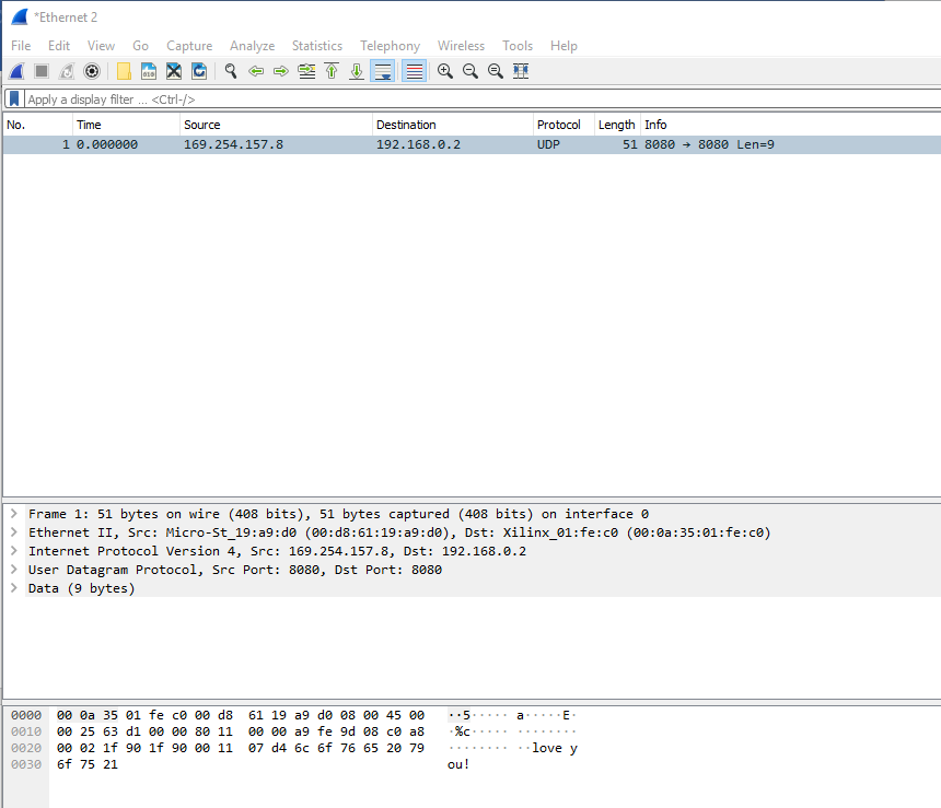
Fig 14. 17 Correct reception of data on the PC side
- Complete Ethernet data transmission design
For complete Ethernet data transmission, it is necessary to have the receiving part of the data and the sending part of the data. For the convenience of experiment, we store the data sent by the PC first in the ram. After reading via the transmitting end, send it to the PC. A series of data unpacking and packaging reference project file “ethernet”. A brief introduction to each module follows.
-
- Data receiving module (ip_receive)
The problem to be solved by this module is to detect and identify the data frame, unpack the valid data frame, and store the real data in the ram.
-
- Data sending module (ip_send)
The main content of this module is to read out the data in the ram and package and send the data with the correct packet protocol type (UDP). Before sending, the data is also checked by CRC.
-
- CRC check module (crc)
The CRC32 check of an IP packet is calculated at the destination MAC Address and is calculated until the last data of a packet. The CRC32 verilog algorithm and polynomial of Ethernet can be generated directly at the following website: http://www.easics.com/webtools/crctool
-
- UDP data test module (UDP)
This module only needs to instantiate the first three sub-modules together, paying attention to the correctness of each connection.
-
- Top level module settings (ethernet)
The PLL, ddio_in, ddio_out, ram, and UDP modules are instantiated to the top layer, and specific information is stored in advance in the ram (Welcome To ZGZNXP World!). When there is no data input, the FPGA always sends this information. With data input, the received data is sent. Refer to the project files for more information.
-
- Compile and download the program to the board
Before the program is verified, it is necessary to note that the IP address of the PC and the MAC address of the development board must be determined and matched, otherwise the data will not be received.
Download the compiled project to the development board. See Fig 14. 18, the FPGA has been sending information to the PC. The entire transmitted packet can also be seen in Wireshark, as shown in Fig 14. 19.
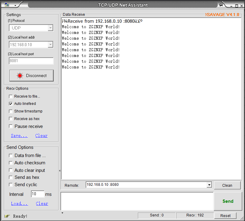
Fig 14. 18 Send the specific information
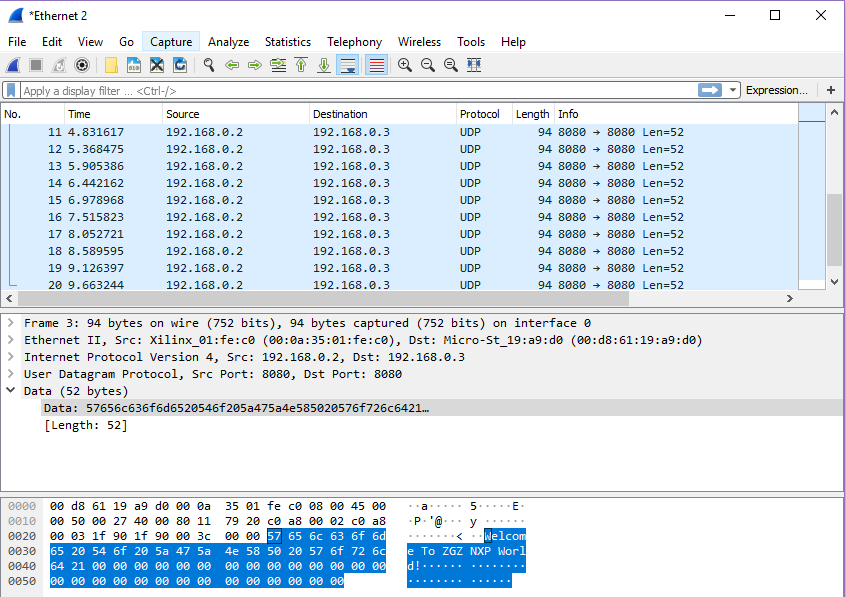
Fig 14. 19 Specific information packet
When the PC sends data to the FPGA, as shown in Fig 14. 20, the entire packet arrives at the FPGA, and then the FPGA repackages the received data and sends it to the PC. See Fig 14. 21, the network assistant also receives the transmitted data information accurately, as shown in Fig 14. 22. Similarly, through SignalTap we can see the process of writing the received data, as shown in Fig 14. 23.

Fig 14. 20 PC sends a packet
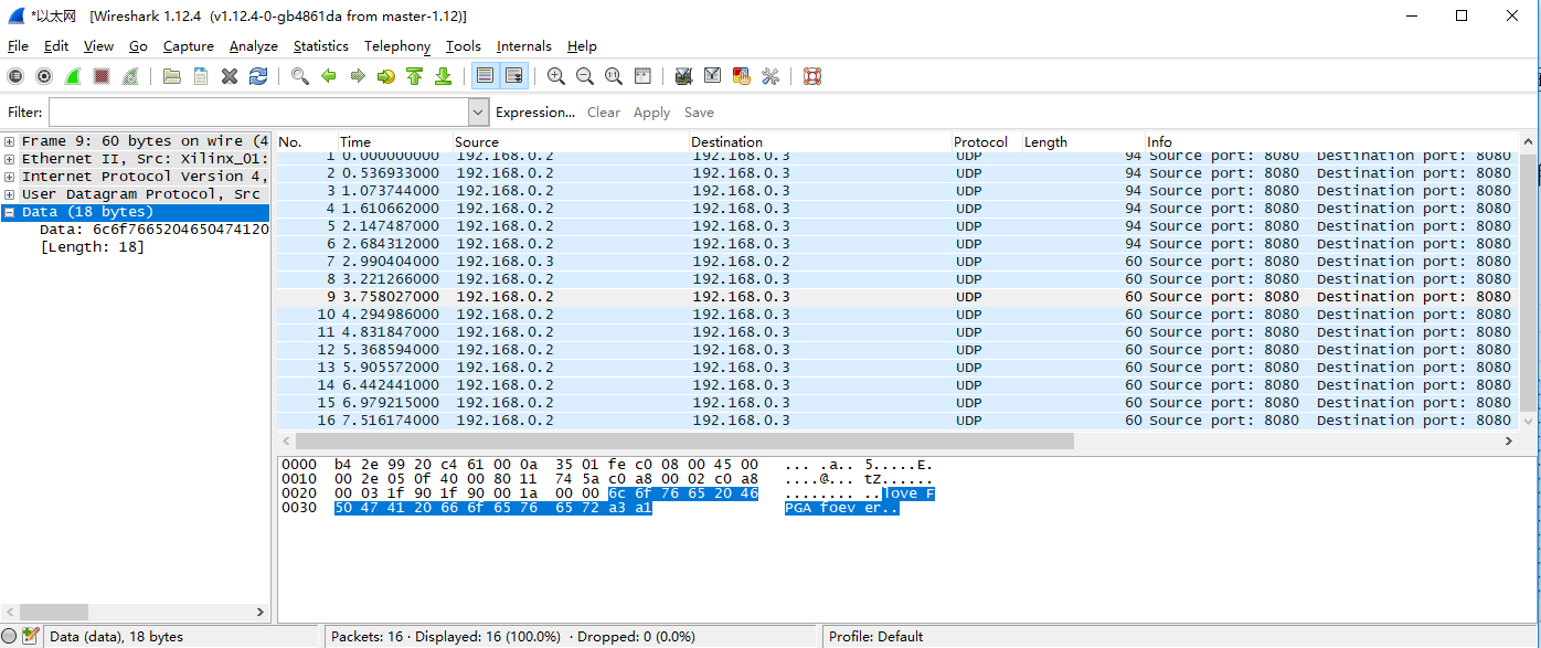
Fig 14. 21 The FPGA repackages the received data and sends it to the PC
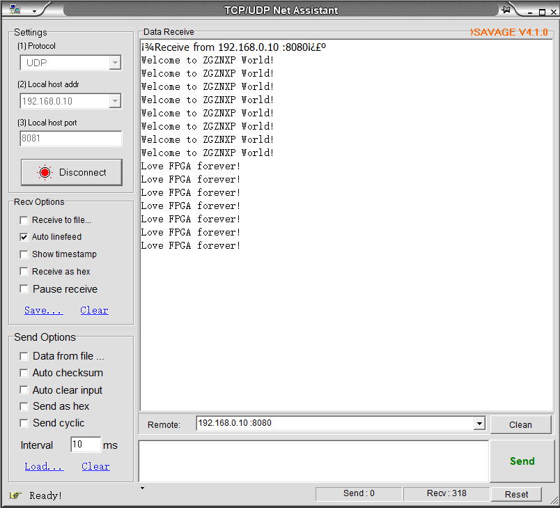
Fig 14. 22 Information received by PC from FPGA
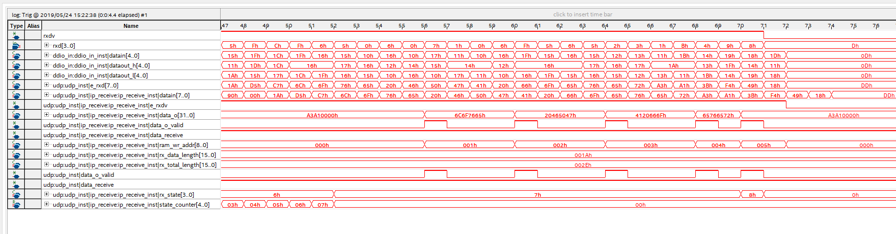
Fig 14. 23 FPGA end data and stored in the ram process
Some Verilog Code maybe helpful to you. If you need more verilog code, please contact us and we can send you in a ZIP file.
set_location_assignment PIN_10 -to rst
set_location_assignment PIN_24 -to rxc
set_location_assignment PIN_28 -to rxd[3]
set_location_assignment PIN_31 -to rxd[2]
set_location_assignment PIN_32 -to rxd[1]
set_location_assignment PIN_33 -to rxd[0]
set_location_assignment PIN_34 -to rxdv
set_location_assignment PIN_43 -to txc
set_location_assignment PIN_46 -to txd[3]
set_location_assignment PIN_49 -to txd[2]
set_location_assignment PIN_50 -to txd[1]
set_location_assignment PIN_51 -to txd[0]
set_location_assignment PIN_42 -to txen
module test1 (rst, rxc, rxdv, rxd, txc, txen, txd, e_mdc, e_mdio);

	input rst;
	input rxc;
	input rxdv;
	input [3:0] rxd;

	output txc;
	output txen;
	output [3:0] txd;

	output e_mdc;
	inout e_mdio;

	assign txd = rxd;
	assign txen = rxdv;
	assign txc = rxc;

//smi_ctrl   camera block
smi_ctrl  smi_ctrl_inst
(
	.sys_clk	(txc),
	.fpga_en	(1'b1),

	.e_mdc		(e_mdc),
	.e_mdio		(e_mdio),

	.smi_done	(),
	.test_pin	(),
	.reset		(rst)
);

endmodule