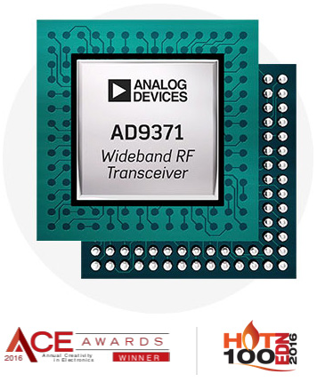
AD9371
ADRV9371-W/PCBZ Compatible RF/IF and RFID FPGA Board -$999 – AD9371 Development Board- FII-BD9371 Board
AD9371 Evaluation Boards
AD9371 Overview
The AD9371 RF transceiver is designed for applications that require high performance radio transmissions across a wideband frequency range, such as 3G/4G Macro BTS, 3G/4G Massive MIMO, and SDR. The AD9371 is packaged in a highly integrated 12mm x 12mm SoC which replaces as many as 20 high performance discrete components.
Introducing the AD9371
 The AD9371 RF transceiver is for applications that require high performance radios across a wideband frequency range while maintaining low power consumption levels. It is a highly integrated 12mm x 12mm SoC that replaces as many as 20 high performance discrete components. The AD9371 covers a 300-MHz to 6-GHz frequency range and supports receiver and transmit large signal instantaneous bandwidths up to 100 MHz, observation receiver and transmit synthesis bandwidths up to 250 MHz, fully integrated LO and clocking functions, and highly advanced on-chip calibration and correction algorithms.
The AD9371 has been widely praised by design thought leaders, winning an ACE Award, an EDN Hot 100 Products Award, a Microwave & RF Top New Products Award, and the Military & Aerospace Electronics Platinum Technology Innovation Award.
Feature and Benefits
- Dual differential transmitters (Tx)
- Dual differential receivers (Rx)
- Observation receiver (ORx) with 2 inputs
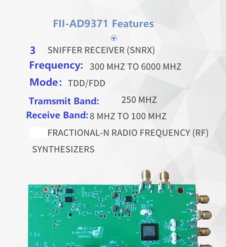
- Sniffer receiver (SnRx) with 3 inputs
- Tunable range: 300 MHz to 6000 MHz
- Tx synthesis bandwidth (BW) to 250 MHz
- Rx BW: 8 MHz to 100 MHz
- Supports frequency division duplex (FDD) and time division duplex (TDD) operation
- Fully integrated independent fractional-N radio frequency (RF) synthesizers for Tx, Rx, ORx, and clock generation
- JESD204B digital interface
Product Details
The AD9371 is a highly integrated, wideband RF transceiver offering dual channel transmitters and receivers, integrated synthesizers, and digital signal processing functions. The IC delivers a versatile combination of high performance and low power consumption required by 3G/4G micro and macro BTS equipment in both FDD and TDD applications. The AD9371 operates from 300 MHz to 6000 MHz, covering most of the licensed and unlicensed cellular bands. The IC supports receiver bandwidths up to 100 MHz. It also supports observation receiver and transmit synthesis bandwidths up to 250 MHz to accommodate digital correction algorithms.
The transceiver consists of wideband direct conversion signal paths with state-of-the-art noise figure and linearity. Each complete receiver and transmitter subsystem includes dc offset correction, quadrature error correction (QEC), and programmable digital filters, eliminating the need for these functions in the digital baseband. Several auxiliary functions such as an auxiliary analog- to-digital converter (ADC), auxiliary digital-to-analog converters (DACs), and general-purpose input/outputs (GPIOs) are integrated to provide additional monitoring and control capability.
An observation receiver channel with two inputs is included to monitor each transmitter output and implement interference mitigation and calibration applications. This channel also connects to three sniffer receiver inputs that can monitor radio activity in different bands.
The high speed JESD204B interface supports lane rates up to 6144 Mbps. Four lanes are dedicated to the transmitters and four lanes are dedicated to the receiver and observation receiver channels.
The fully integrated phase-locked loops (PLLs) provide high performance, low power fractional-N frequency synthesis for the transmitter, the receiver, the observation receiver, and the clock sections. Careful design and layout techniques provide the isolation demanded in high performance base station applications. All voltage controlled oscillator (VCO) and loop filter components are integrated to minimize the external component count.
A 1.3 V supply is required to power the core of the AD9371, and a standard 4-wire serial port controls it. Other voltage supplies provide proper digital interface levels and optimize transmitter and auxiliary converter performance. The AD9371 is packaged in a 12 mm × 12 mm, 196-ball chip scale ball grid array (CSP_BGA).
Applications
- 3G/4G micro and macro base stations (BTS)
- 3G/4G multicarrier picocells
- FDD and TDD active antenna systems
- Microwave, nonline of sight (NLOS) backhaul systems
SDR Integrated Transceiver Design Resources
The AD9371 User Guide UG-992 contains user information regarding the Zynq carrier board EVAL-TPG-ZYNQ3 in the section “AD9371 Demonstration System Overview.”
Guidelines for obtaining technical support are as follows:
- All schematics, layout recommendations, and specifications in the design package have been verified and insure optimum performance from the transceivers. Adherence to these specifications is necessary in order to achieve the device’s rated performance in your design.
- The evaluation boards are fully characterized by ADI. If you encounter an issue with your design, you must be able to recreate the issue on the ADI evaluation platform.
- Questions related to clarification of the content provided in the design file package should be posted on the community forum and will be addressed by the ADI response team. Questions outside of the scope of the design resources provided cannot be supported.
Download the AD9361 Design File Package
(Last Updated 12/2017)
Requires registration
Download the AD9371 Design File Package
(Last Updated 12/2017)
Requires registration
AD9371, AD9375 highly integrated, wideband RF transceiver Linux device driver
 The AD9371 AD9375 is a highly integrated, wideband RF transceiver offering dual channel transmitters and receivers, integrated synthesizers, and digital signal processing functions. The IC delivers a versatile combination of high performance and low power consumption required by 3G/4G micro and macro base station equipment in both FDD and TDD applications. The AD9371 operates from 300 MHz to 6000 MHz, covering most of the licensed and unlicensed cellular bands. The IC supports receiver bandwidths up to 100 MHz. It also supports observation receiver and transmit synthesis bandwidths up to 250 MHz to accommodate digital correction algorithms. The transceiver consists of wideband direct conversion signal paths with state-of-the-art noise figure and linearity. Each complete receiver and transmitter subsystem includes dc offset correction, quadrature error correction, and programmable digital filters, eliminating the need for these functions in the digital baseband. Several auxiliary functions such as an auxiliary analog-to-digital converter (ADC), auxiliary digital-to-analog converters (DACs), and general-purpose input/outputs (GPIOs) are integrated to provide additional monitoring and control capability. An observation receiver channel with two inputs is included to monitor each transmitter output and implement interference mitigation and calibration applications. This channel also connects to three sniffer receiver inputs that can monitor radio activity in different bands.
The AD9375 device variant provides digital signal processing capabilities in the embedded ARM processor using closed-loop feedback signals from the observation receiver channels. These functions improve transmitter performance, measure system output, and reduce system power consumption. The list of functions includes the following: digital predistortion (DPD), closed-loop gain control (CLGC), and voltage standing wave ratio (VSWR) measurement.
Description
This is a Linux industrial I/O (IIO) subsystem driver, targeting RF Transceivers. The industrial I/O subsystem provides a unified framework for drivers for many different types of converters and sensors using a number of different physical interfaces (i2c, spi, etc). See IIO for more information.
MATLAB Profile Generator for AD9371
The AD9371 Filter Design Wizard is used to design the transmitter and receiver FIR filters for the AD9371 product family. It can also be used with the AD9375 device. This tool creates filters which equalize the desired passband, taking into account the signal transfer functions through the entire analog and digital signal path in the AD9371 transceiver. The tool also generates ADC profiles and custom clock settings that can be used with the Transceiver Evaluation Software to evaluate system performance. Any custom configuration of sampling rates and bandwidths must use this tool to create a profile that can be used by in a customer system or with the evaluation kit. The Filter Wizard is available as MATLAB source code, a MATLAB app, and as a stand-alone executable.
With this wizard, users can perform the following tasks:
-
Design the programmable FIR filters, get the filter coefficients and save them to a file, which can be directly loaded into the hardware.
-
Examine the independent response of each filter, and the composite response of all the filters in a channel, including both digital and analog filters.
-
Generate custom clock settings that can be used to evaluate performance of using different device clock inputs and sample rates.
How RadioVerse’s AD9371 Leads the Transceiver Market
High Performance and Integration
- Replaces as many as 20 high performance, discrete radio components with one SOC solution providing simple, reliable connections.
- Direct conversion, high linearity, and self calibration maintain best performance levels under varying environmental and operating conditions.
- Large-scale integration and zero IF allows for wide frequency range and eliminates interconnection losses while reducing broadband matching concerns.
Versatility
- Offers a common SDR platform for a wide range of applications, reducing development time and inventory costs.
- Operates from 300 MHz to 6 GHz.
- Supports receiver bandwidths up to 100 MHz.
- Supports operating transmit bandwidths up to 100 MHz and observation receiver and transmit synthesis bandwidths up to 250 MHz for digital correction algorithms.
Size, Weight, and Power (SWaP)
- Reduced component count enables radios to be installed on buildings, light poles, office walls, and more.
- A power consumption level at less than 5 W under normal operating conditions reduces the need for cooling, increases reliability, and reduces operating costs.
- JESD204B data interface minimizes input/output lines, reduces routing density making PCB routing easier.
Ease of Use
- ADI radio technology design expertise reduces development costs and time to market (TTM).
- Complete API, software user guides, and a standard serial peripheral interface (SPI) simplify development.
- On-chip tracking calibration maintains performance with little user control required.
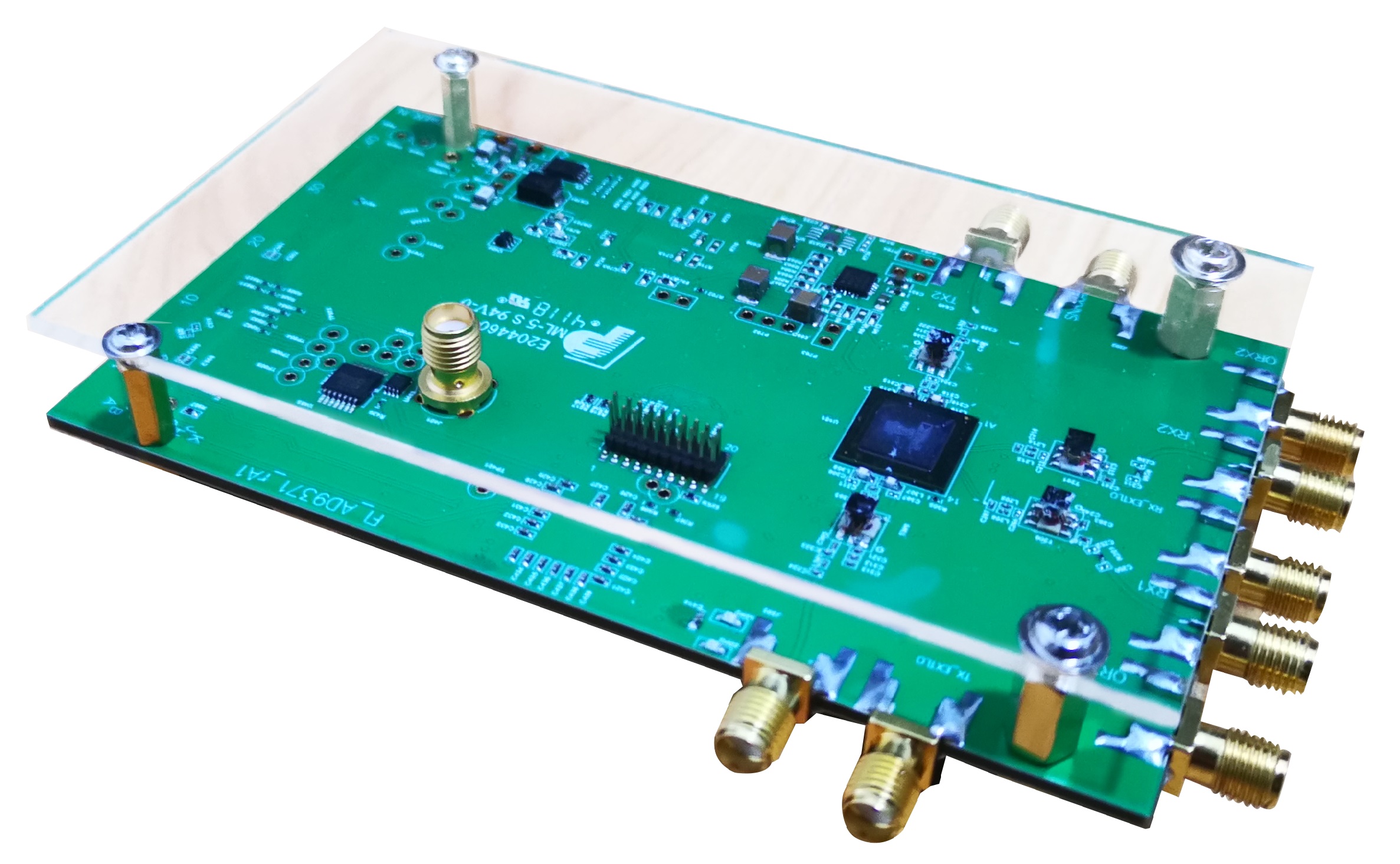
AD9371 Evaluation Boards
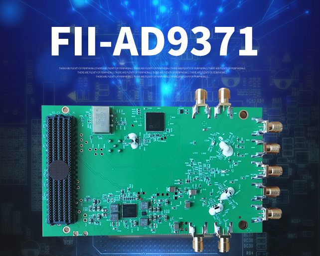
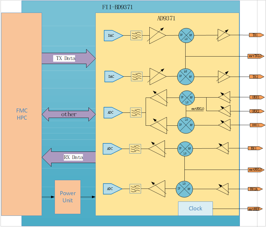
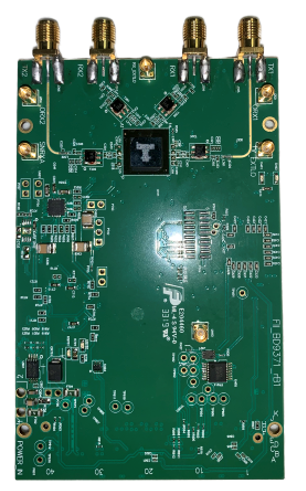
FII-AD9371 (completely compatible with ADRV9371-W/PCBZ ) are radio cards designed to showcase the AD9371, a high performance wideband integrated RF transceiver intended for use in RF applications such as 4G basestation, test and measurement applications and software defined radios.
FII-BD9371 (completely compatible with ADRV9371-W/PCBZ board ) is a single board with integrated transceiver AD9371 and its supporting power supply, radio frequency and digital interface, which is a high-performance, highly integrated RF transceiver board, suitable for 3G to 5G base station and test equipment, software-defined radio SDR and other RF application fields, the programmability and broadband capabilities of the module make it an ideal choice for a variety of transceiver applications. Transceiver For Use With AD9371, AD9528, ADP5054.
2. The module sets the RF front end, mixer, frequency synthesizer and high-speed analog-to-digital conversion device to provide a configurable FMC-HPC digital interface for the processor or FPGA, thereby simplifying the design. The operating frequency range of the RF chip is 300 MHz to 6 GHz, and the single channel bandwidth range is up to 100 MHz.
The radio cards provide hardware engineers, software engineers and system architects with a single 2×2 transceiver platform for device evaluation and rapid prototyping of radio solutions. All peripherals necessary for the radio card to operate including a high efficiency switcher only power supply solution, and a high performance clocking solution are populated on the board.
- Complete Radio Card platform containing AD9371 with:
- 2 x Transmit outputs
- 2 x Receive inputs
- 2 x Observation inputs
- 1x Sniffer path
- Narrow tuning range and Wide tuning range options
- ADRV9371-W/PCBZ matched for 300MHz – 6GHz
- Complete with high efficiency power supply solution and clocking solution for AD9371
- FMC connector to Xilinx ZC706 motherboard (EK-Z7-ZC706-G).
- Powered from single FMC connector
- Includes schematics, layout, BOM, HDL, drivers and application software
| Frequency | 300MHz ~ 6GHz |
|---|
| Type | Transceiver |
|---|
| Base Part Number | ADRV9371 |
|---|
| For Use With/Related Products | AD9371, AD9528, ADP5054 |
|---|

Hardware specifications and indicators
1. Appearance and physical size
 BD9371 physical picture (without protective cover)
110CM X 70CM
2.Board hardware RF parameter index
| Hardware RF parameter specifications | Hardware index |
| Transmission frequency range | 300 MHz to 6 GHz |
| Receive frequency range | 300 MHz to 6 GHz |
| RF bandwidth | 200 kHz to 100 MHz |
| Adjustable range of transmission gain | 40dB |
| Tunable receive gain | 30dB |
| Maximum transmit power | 0-5dBm |
| Number of transmitting channels | 2 |
| Number of receiving channels | 2 |
3. Working environment parameter index
| Work environment project specifications | Hardware index |
| Power supply | 12V |
| Operating temperature | -20℃ to 45℃ |
| humidity | 2%~98%(Normal temperature) |
| Power consumption | Typical value 9.0W |
Advantages and Features:
1. Tunable transmit and receive frequencies: transmit: 300 MHz to 6 GHz, receive: 300 MHz to 6 GHz
2. Tunable transmit and receive bandwidth: 200 kHz to 100 MHz
3. The transmit power and receive gain can be tuned: transmit: >40dB receive: >30dB
4. High transmit power and good broadband flatness, better than similar products on the market.
5. Power supply and data transmission through standard FMC-HPC connector
6. Support MIMO function, 2 channels transmit and 2 channels receive
7. Can be combined with FII-BM7100 or other platforms that support FMC interface for software radio applications
| Datasheets |
|---|
Video FileGNU Radio Conference 2016 – Radio Architecture Design Challenges
AD9371 – Filter and Signal Path Configuration
Profiles
AD9371 uses profiles to designate different device configuration settings for the Tx/Rx/ORx/SnRx channels. When selecting a profile, note that Rx1 and Rx2 use the same profile; Tx1 and Tx2 use the same profile; ORx1 and ORx2 use the same profile; and SnRxA, SnRxB, and SnRxC use the same profile. The profile dictates how the digital filters, analog filters, clock rates, and clock dividers are configured in the device. Some specific parameters set by profiles include the IQ data rate, ADC clock rate, analog filter corners, FIR filter coefficients, and interpolation/decimation factors in the half band filters. Several profiles can be examined in the AD9371 Transceiver Evaluation Software for given device clock frequencies. If the desired profile exists in the software, it is recommended to setup the desired profile in and use the data structure values generated by the “Create Config.c File” button for the Tx/Rx/ORx/SnRx profile data structures.
RX Signal Path
The AD9371 contains dual receiver channels. Each Rx channel is a direct conversion system that contains a programmable attenuator stage, followed by matched I and Q mixers that down convert received signals to baseband for digitization. To achieve gain control, a programmed gain index map is implemented. This gain map distributes attenuation among the various Rx blocks for optimal performance at each power level. In addition, support is available for both automatic and manual gain control modes. The receiver includes S-? ADCs and adjustable sample rates that produce data streams from the received signals. The signals can be conditioned further by a series of decimation filters and a fully programmable 72-tap FIR filter with additional decimation settings. The sample rate of each digital filter block is adjustable by changing the decimation factors to produce the desired output data rate.
Observation RX Signal Path
The ORx operates in a similar manner to the main receivers. Each input is differential and uses a dedicated mixer. The ORx inputs share a baseband ADC and baseband section; therefore, only one can be active at any time. The mixed signal and digital section is identical in design and operation to the main receiver channels. This channel can monitor the Tx channels and implement error correction functions. It can also be used as a general-purpose receiver.
Setting the Observation Path Source
When the ARM radio control is in ARM command mode, this attribute allows the user to selectively power-up or power-down the desired ObsRx data path.
-
OFF – SnRx path is disabled
-
ORX1_TX_LO – SnRx operates in observation mode on ORx1 with Tx LO synthesizer
-
ORX2_TX_LO – SnRx operates in observation mode on ORx2 with Tx LO synthesizer
-
INTERNALCALS – enables scheduled Tx calibrations while using SnRx path. The enableTrackingCals function needs to be called in RADIO_OFF state. It sets the calibration mask, which the scheduler will later use to schedule the desired calibrations. This command is issued in RADIO_OFF. Once the AD9371 moves to RADIO_ON state, the internal scheduler will use the enabled calibration mask to schedule calibrations whenever possible, based on the state of the transceiver. The Tx calibrations will not be scheduled until INTERNALCALS is selected and the Tx calibrations are enabled in the cal mask.
-
OBS_SNIFFER – SnRx operates in sniffer mode with latest selected Sniffer Input – for hardware pin control operation. In pin mode, the GPIO pins designated for ORX_MODE would select SNIFFER mode. Then MYKONOS_setSnifferChannel function would choose the channel.
-
ORX1_SN_LO – SnRx operates in observation mode on ORx1 with SNIFFER LO synthesizer
-
ORX2_SN_LO – SnRx operates in observation mode on ORx2 with SNIFFER LO synthesizer
-
SN_A – SnRx operates in sniffer mode on SnRxA with SNIFFER LO synthesizer
-
SN_B – SnRx operates in sniffer mode on SnRxB with SNIFFER LO synthesizer
-
SN_C – SnRx operates in sniffer mode on SnRxC with SNIFFER LO synthesizer
TX Signal Path
The AD9371 employs a direct conversion transmitter architecture consisting of two identical and independently controlled channels that provide all the digital processing, mixed signal, and RF blocks necessary to implement a direct conversion system. Both channels share a common frequency synthesizer. The digital data from the JESD204B lanes pass through a fully programmable 96-tap FIR filter with optional interpolation. The FIR output is sent to a series of conversion filters that provide additional filtering and data rate interpolation prior to reaching the DAC. Each DAC has an adjustable sample rate and is linear up to full scale. Once converted to baseband analog signals, the in-phase (I) and quadrature (Q) signals are filtered to remove sampling artifacts, and then the signals are fed to the upconversion mixers. At the mixer stage, the I and Q signals are recombined and modulated onto the carrier frequency for transmission to the output stage. Each transmit chain provides a wide attenuation adjustment range with fine granularity to help designers optimize SNR.
RX Gain Control
The AD9371 main receivers (Rx1, Rx2) and sniffer receivers (SnRxA, SnRxB, SnRxC) feature automatic and manual gain control modes that provide flexible gain control in a wide array of applications. Observation receivers (ORx1, ORx2) feature Manual Gain Control (MGC) only. Automatic Gain Control (AGC) allows the receivers to autonomously adjust receiver gain depending on variations of the input signal, such as the onset of a strong interferer overloading the receiver data path. All the receivers are also capable of operating in MGC mode where changes in gain are initiated by the Baseband Processor (BBP) over SPI or GPIO.
The default gain tables can be found in the mykonos_user.c file, and are loaded by default. Custom gain tables can be loaded automatically during driver probe or anytime later via the gain_table_config sysfs attribute. Tables must be stored in the /lib/firmware folder, or compiled into the kernel using the CONFIG_FIRMWARE_IN_KERNEL, CONFIG_EXTRA_FIRMWARE config options. The table loaded during driver probe can be specified using following device tree property:
adi,gaintable-name = “ad9371_std_gaintable”;
In case no table is specified or loaded, the driver will continue to use the provided standard gain tables.
Gain tables are stored in a human readable file, with the format specified below.
Gain control modes
The AD9371 Rx supports three modes of gain control. These modes are described in brief below:
| Mode | Description |
|---|---|
| Manual Gain Control (MGC) | Provides the user full control over the current gain index. In MGC, the gain index can be controlled in two ways: through API commands and through GPIO signaling. |
| Hybrid Mode | When the user sends a pulse to a GPIO pin enabled as the Hybrid Mode Gain Change pin, the AGC overload counters are polled to determine if a gain increase or decrease is necessary. When the pulse is registered by the gain control block a gain increase is made in the case of an underrange scenario, a gain decrease is made in the case of an overrange signal, or no gain change is made. This mode allows the user to determine when gain changes occur. The Hybrid Mode is a subset of AGC as Hybrid Mode uses many of the same circuits, thresholds, and counter parameters as AGC. |
| Automatic Gain Control (AGC) | The AGC will determine when gain changes should be made. There are several configurations that can be used in AGC. Examples include the option to reduce gain as soon as an overrange has been detected (fast attack mode), change gain (if necessary) only at the expiry of a variable length counter (AGC gain update counter, operating without fast attack), synchronization of the counter to an external pulse (AGC enable sync pulse), and others. . |