Understand the register configuration of the ADV7511, HDMI Graphic Display Experiment – Xilinx Risc-V Board Tutorial : FII-PRX100 FPGA Board Experiment 14
Experiment 14 HDMI Graphic Display Experiment
1.Experiment Objective
- Learn about video timing
(2) Understand the register configuration of the ADV7511, reviewing the knowledge from experiment 12
2.Experiment Requirement
- Image display processing has always been the focus of FPGA research. At present, the image display mode is also developing. The image display interface is also gradually transitioning from the old VGA interface to the new DVI or HDMI interface.
- Display the image using the HDMI interface of the development board.
- Download the program to the board for comparison.
- Introduction to HDMI: HDMI (High Definition Multimedia Interface) is a digital video/audio interface technology. It is a dedicated digital interface for image transmission. It can transmit audio and video signals at the same time. The highest data transmission speed is 48 Gbps (version 2.1).
- Introduction to ADV7511: The ADV7511 is a chip that can convert VGA timing to HDMI timing. For more details, see the related chip manual. Among them, “ADV7511 Programming Guide” and “ADV7511 Hardware Users Guide” are the most important. From Table 16 on page 27 of “ADV7511 Programming Guide”, the bit width and format type of RGB can be configured. Its registers can output the appropriate format according to needs after configuration.
- ADV7511 Register Configuration Description: The bus inputs D0-D3, D12-D15, and D24-D27 of the ADV7511 have no input, that is, RGB4:4:4, and each bit of data is in 8-bit mode. Directly set 0x15 [3:0] to 0x0. Set [5:4] of 0X16 to 11 and keep the default values for the other digits. 0x17[1] refers to the ratio of the length to the width of the image. It can be set to 0 or 1. The actual LCD screen will not change according to the data, but will automatically stretch the full screen mode according to the LCD’s own settings. 0x18[7] is the way to start the color range stretching. The design is that RGB maps directly to RGB, so it can be disabled directly. 0XAF[1] is the setting of choosing either HDMI or DVI mode. The most direct point of HDMI over DVI is that HDMI can send digital audio data and encrypt data content. This experiment only needs to display the picture, and it can be set directly to DVI mode. 0XAF[7], set to 0 to turn off HDMI encryption. Due to GCCD, deep color encryption data is not applicable, so the GC option is turned off. 0xAF[7] is set to 0 to turn off the GC CD data.
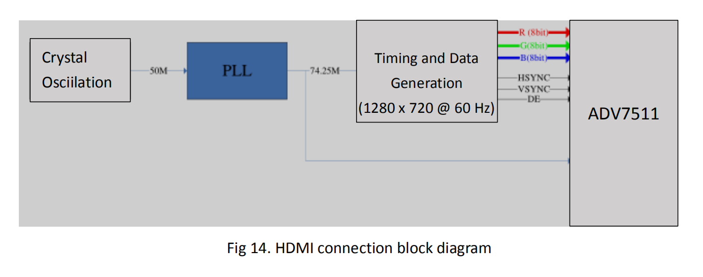
Fig 14. HDMI connection block diagram
3.Program Design
3.1 Schematics
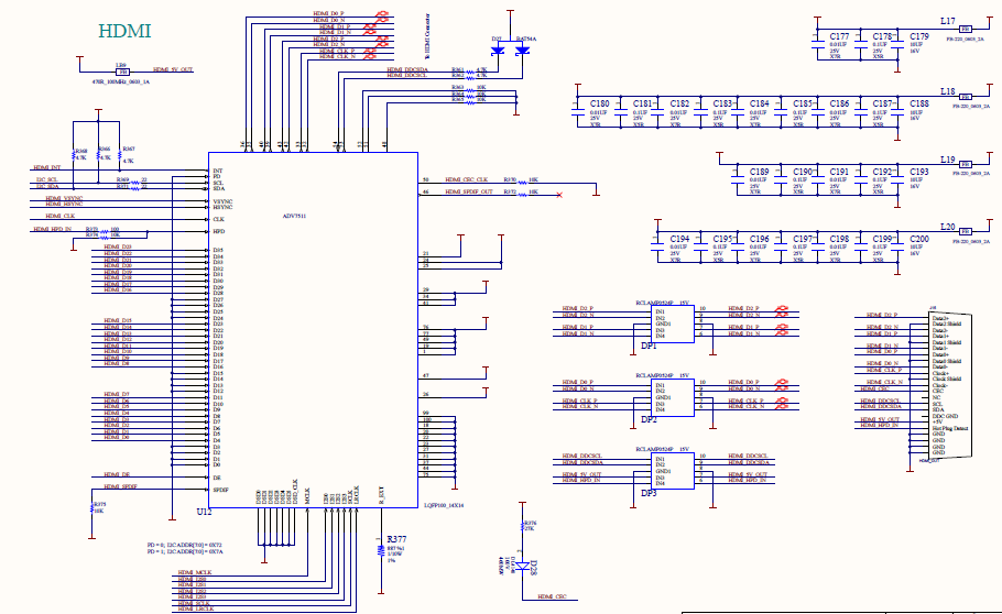
Fig 14. 2 Schematics of ADV7511
3.2 Main Code
-
- 1080p VGA main part of the timing generation program
| // Set horizontal scanning parameter 1920*1080 60Hz VGA Clock bit 130 MHz
//———————————————————–// parameter LinePeriod =2000; parameter H_SyncPulse=12; parameter H_BackPorch=40; parameter H_ActivePix=1920; parameter H_FrontPorch=28; parameter Hde_start=52; parameter Hde_end=1972; //———————————————————–//
//———————————————————–// parameter FramePeriod =1105; parameter V_SyncPulse=4; parameter V_BackPorch=18; parameter V_ActivePix=1080; parameter V_FrontPorch=3; parameter Vde_start=22; parameter Vde_end=1102; reg [12 : 0] x_cnt; reg [10 : 0] y_cnt; reg [23 : 0] grid_data_1; reg [23 : 0] grid_data_2; reg [23 : 0] bar_data; reg [3 : 0] vga_dis_mode; reg [7 : 0] vga_r_reg; reg [7 : 0] vga_g_reg; reg [7 : 0] vga_b_reg; reg hsync_r; reg vsync_r; reg hsync_de; reg vsync_de; reg [15:0] key1_counter; reg rst ; wire [12:0] bar_interval;
assign bar_interval = H_ActivePix[15: 3];
always @ (posedge vga_clk) rst<= !loceed ; always @ (posedge vga_clk) if(rst) x_cnt <= 1; else if(x_cnt == LinePeriod) x_cnt <= 1; else x_cnt <= x_cnt+ 1;
//—————————————————————- //—————————————————————- always @ (posedge vga_clk) begin if(rst) hsync_r <= 1’b1; else if(x_cnt == 1) hsync_r <= 1’b0; else if(x_cnt == H_SyncPulse) hsync_r <= 1’b1;
if(rst) hsync_de <= 1’b0; else if(x_cnt == Hde_start) hsync_de <= 1’b1; else if(x_cnt == Hde_end) hsync_de <= 1’b0; end always @ (posedge vga_clk) if(rst) y_cnt <= 1; else if(y_cnt == FramePeriod) y_cnt <= 1; else if(x_cnt == LinePeriod) y_cnt <= y_cnt+1; always @ (posedge vga_clk) begin if(rst) vsync_r <= 1’b1; else if(y_cnt == 1) vsync_r <= 1’b0; else if(y_cnt == V_SyncPulse) vsync_r <= 1’b1;
if(rst) vsync_de <= 1’b0; else if(y_cnt == Vde_start) vsync_de <= 1’b1; else if(y_cnt == Vde_end) vsync_de <= 1’b0; end
assign en = hsync_de & vsync_de ; always @(posedge vga_clk) begin if ((x_cnt[4]==1’b1) ^ (y_cnt[4]==1’b1)) grid_data_1<= 24’h000000; else grid_data_1<= 24’hffffff;
if ((x_cnt[6]==1’b1) ^ (y_cnt[6]==1’b1)) grid_data_2<=24’h000000; else grid_data_2<=24’hffffff;
end always @(posedge vga_clk) begin if (x_cnt==Hde_start) bar_data<= 24’hff0000; //Red strip else if (x_cnt==Hde_start + bar_interval) bar_data<= 24’h00ff00; //Green strip else if (x_cnt==Hde_start + bar_interval*2) bar_data<=24’h0000ff; //Blue strip else if (x_cnt==Hde_start + bar_interval*3) bar_data<=24’hff00ff; //Purple strip else if (x_cnt==Hde_start + bar_interval*4) bar_data<=24’hffff00; //Yellow strip else if (x_cnt==Hde_start + bar_interval*5) bar_data<=24’h00ffff; //Light blue strip else if (x_cnt==Hde_start + bar_interval*6) bar_data<=24’hffffff; //White strip else if (x_cnt==Hde_start + bar_interval*7) bar_data<=24’hff8000; //Orange strip else if (x_cnt==Hde_start + bar_interval*8) bar_data<=24’h000000; //Black strip end always @(negedge vga_clk) if(rst) begin vga_r_reg<=0; vga_g_reg<=0; vga_b_reg<=0; end else case(vga_dis_mode) 4’b0000:begin vga_r_reg<=0; //VGA dispaly all black vga_g_reg<=0; vga_b_reg<=0; end 4’b0001:begin vga_r_reg<=8’hff; //VGA dispaly all white vga_g_reg<=8’hff; vga_b_reg<=8’hff; end 4’b0010:begin vga_r_reg<=8’hff; //VGA dispaly all red vga_g_reg<=0; vga_b_reg<=0; end 4’b0011:begin vga_r_reg<=0; //VGA dispaly all green vga_g_reg<=8’hff; vga_b_reg<=0; end 4’b0100:begin vga_r_reg<=0; //VGA dispaly all blue vga_g_reg<=0; vga_b_reg<=8’hff; end 4’b0101:begin vga_r_reg<=grid_data_1[23:16]; // VGA display squre 1 vga_g_reg<=grid_data_1[15:8]; vga_b_reg<=grid_data_1[7:0]; end 4’b0110:begin vga_r_reg<=grid_data_2[23:16]; // VGA display squre 2 vga_g_reg<=grid_data_2[15:8]; vga_b_reg<=grid_data_2[7:0]; end 4’b0111:begin vga_r_reg<=x_cnt[12:5]; // VGA display horizontal gradient vga_g_reg<=x_cnt[12:5]; vga_b_reg<=x_cnt[12:5]; end 4’b1000:begin vga_r_reg<=y_cnt[10:3]; // VGA display vertical gradient vga_g_reg<=y_cnt[10:3]; vga_b_reg<=y_cnt[10:3]; end
4’b1001:begin vga_r_reg<=x_cnt[12:5]; // VGA display red horizontal gradient vga_g_reg<=0; vga_b_reg<=0; end 4’b1010:begin vga_r_reg<=0; // VGA display green horizontal gradient vga_g_reg<=x_cnt[12:5]; vga_b_reg<=0; end 4’b1011:begin vga_r_reg<=0; // VGA display blue horizontal gradient vga_g_reg<=0; vga_b_reg<=x_cnt[12:5]; end 4’b1100:begin vga_r_reg<=bar_data[23:16]; //VGA display colorful strips vga_g_reg<=bar_data[15:8]; vga_b_reg<=bar_data[7:0]; end default:begin vga_r_reg<=8’hff; //VGA display all white vga_g_reg<=8’hff; vga_b_reg<=8’hff; end endcase;
assign vga_hs = hsync_r; assign vga_vs = vsync_r; assign vga_r = (hsync_de & vsync_de)?vga_r_reg:8’h00; assign vga_g = (hsync_de & vsync_de)?vga_g_reg:8’b00; assign vga_b = (hsync_de & vsync_de)?vga_b_reg:8’h00; |
-
- Main part of register configuration
Directly use the above experimental content for IIC interface configuration register. Here is mainly about the register configuration part
| case( i )
0: if( iic_done ) begin isStart <= 2’b00; i <= i + 1’b1; end else begin isStart <= 2’b01; rData <= 8’h50; rAddr <= 8’h41; end
1: if( iic_done ) begin isStart <= 2’b00; i <= i + 1’b1; end else begin isStart <= 2’b01; rData <= 8’h10; rAddr <= 8’h41; end
2: if( iic_done ) begin isStart <= 2’b00; i <= i + 1’b1; end else begin isStart <= 2’b01; rData <= 8’h03; rAddr <= 8’h98; end
3: if( iic_done ) begin isStart <= 2’b00; i <= i + 1’b1; end else begin isStart <= 2’b01; rData <= 8’h03; rAddr <= 8’h9a; end
4: if( iic_done ) begin isStart <= 2’b00; i <= i + 1’b1; end else begin isStart <= 2’b01; rData <= 8’h30; rAddr <= 8’h9c; end 5: if( iic_done ) begin isStart <= 2’b00; i <= i + 1’b1; end else begin isStart <= 2’b01; rData <= 8’h01; rAddr <= 8’h9d; end 6: if( iic_done ) begin isStart <= 2’b00; i <= i + 1’b1; end else begin isStart <= 2’b01; rData <= 8’ha4; rAddr <= 8’ha2; end 7: if( iic_done ) begin isStart <= 2’b00; i <= i + 1’b1; end else begin isStart <= 2’b01; rData <= 8’ha4; rAddr <= 8’ha3; end
8: if( iic_done ) begin isStart <= 2’b00; i <= i + 1’b1; end else begin isStart <= 2’b01; rData <= 8’hd0; rAddr <= 8’he0; end
9: if( iic_done ) begin isStart <= 2’b00; i <= i + 1’b1; end else begin isStart <= 2’b01; rData <= 8’h00; rAddr <= 8’hf9; end 10: if( iic_done ) begin isStart <= 2’b00; i <= i + 1’b1; end else begin isStart <= 2’b01; rData <= 8’h20; rAddr <= 8’h15; end
11: if( iic_done ) begin isStart <= 2’b00; i <= i + 1’b1; end else begin isStart <= 2’b01; rData <= 8’h30; rAddr <= 8’h16; end
12: if( iic_done ) begin isStart <= 2’b00; i <= i + 1’b1; end else begin isStart <= 2’b01; rAddr <= 8’haf; rData <= 8’h02;end
13: if( iic_done ) begin isStart <= 2’b00; i <= i + 1’b1; end else begin isStart <= 2’b01; rAddr <= 8’h01; rData <= 8’h00;end
14: if( iic_done ) begin isStart <= 2’b00; i <= i + 1’b1; end else begin isStart <= 2’b01; rAddr <= 8’h02; rData <= 8’h18;end
15: if( iic_done ) begin isStart <= 2’b00; i <= i + 1’b1; end else begin isStart <= 2’b01; rAddr <= 8’h03; rData <= 8’h00;end
16: if( iic_done ) begin isStart <= 2’b00; i <= i + 1’b1; end else begin isStart <= 2’b01; rAddr <= 8’h0a; rData <= 8’h03;end
17: if( iic_done ) begin isStart <= 2’b00; i <= i + 1’b1; end else begin isStart <= 2’b01; rAddr <= 8’h0b; rData <= 8’h6e;end
18: if( iic_done ) begin isStart <= 2’b00; i <= i + 1’b1; end else begin isStart <= 2’b01; rAddr <= 8’h0c; rData <= 8’hbd;end
19: if( iic_done ) begin isStart <= 2’b00; i <= i + 1’b1; end else begin isStart <= 2’b01; rAddr <= 8’hd6; rData <= 8’hc0;end
endcase |
4.Download the Program to the Board to Test
- Lock the pins
| Signal Name | Port Description | Network Label | FPGA Pin |
| clk_in | System clock, 50 MHz | C10_50MCLK | U22 |
| rst_n | Reset, high by default | KEY1 | M4 |
| vga_hs | Horizontal synchronous signal | HDMI_HSYNC | C24 |
| vga_vs | Vertical synchronous signal | HDMI_VSYNC | A25 |
| en | Date valid | HDMI_DE | A24 |
| vga_clk | Display clock | HDMI_CLK | B19 |
| key1 | Display effect toggle button | KEY2 | L4 |
| scl | ADV7511 configuration clock | I2C_SCL | R20 |
| sda | ADV7511 configuration data | I2C_SDA | R21 |
| vag_r[7] | Red output | HDMI_D23 | F15 |
| vag_r[6] | Red output | HDMI_D22 | E16 |
| vag_r[5] | Red output | HDMI_D21 | D16 |
| vag_r[4] | Red output | HDMI_D20 | G17 |
| vag_r[3] | Red output | HDMI_D19 | E17 |
| vag_r[2] | Red output | HDMI_D18 | F17 |
| vag_r[1] | Red output | HDMI_D17 | C17 |
| vag_r[0] | Red output | HDMI_D16 | A17 |
| vag_g[7] | Green output | HDMI_D15 | B17 |
| vag_g[6] | Green output | HDMI_D14 | C18 |
| vag_g[5] | Green output | HDMI_D13 | A18 |
| vag_g[4] | Green output | HDMI_D12 | D19 |
| vag_g[3] | Green output | HDMI_D11 | D20 |
| vag_g[2] | Green output | HDMI_D10 | A19 |
| vag_g[1] | Green output | HDMI_D9 | B20 |
| vag_g[0] | Green output | HDMI_D8 | A20 |
| vag_b[7] | Blue output | HDMI_D7 | B21 |
| vag_b[6] | Blue output | HDMI_D6 | C21 |
| vag_b[5] | Blue output | HDMI_D5 | A22 |
| vag_b[4] | Blue output | HDMI_D4 | B22 |
| vag_b[3] | Blue output | HDMI_D3 | C22 |
| vag_b[2] | Blue output | HDMI_D2 | A23 |
| vag_b[1] | Blue output | HDMI_D1 | D21 |
| vag_b[0] | Blue output | HDMI_D0 | B24 |
- Comprehensive compilation and downloading the program to the board. Each time you press the UP button on the development board, you can see the different display effects on the computer monitor to switch. The effect is as follows:
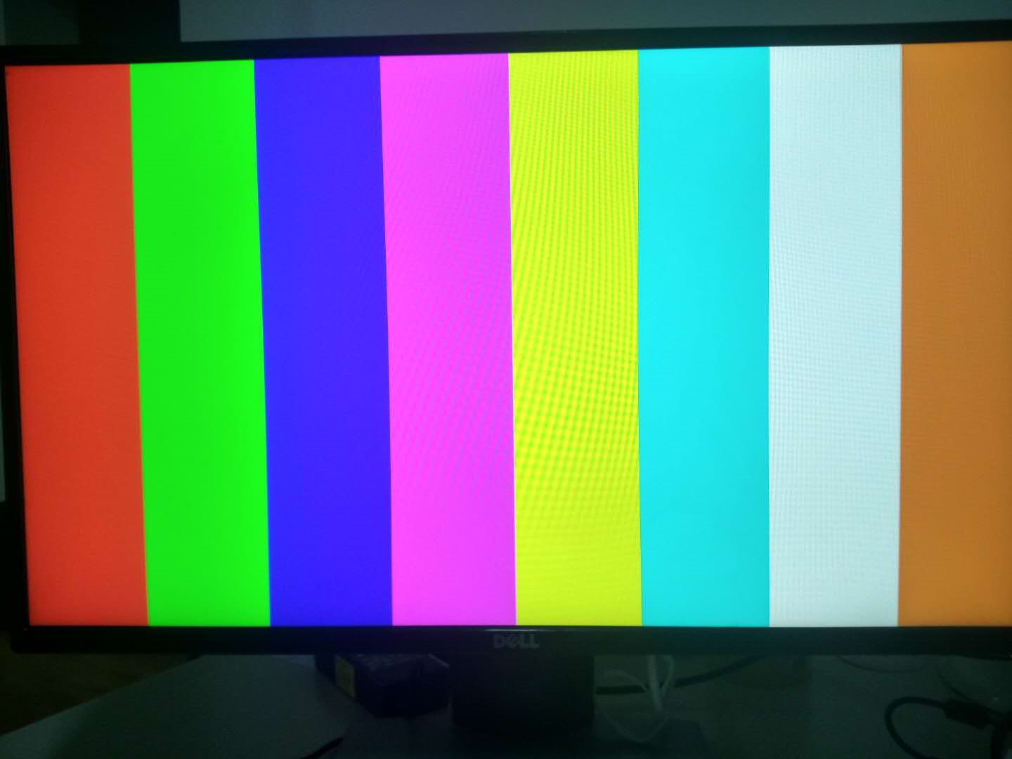
Fig 14. 3 HDMI display