Design 16 outputs ROM, Study the format of *.mif and how to edit *.mif file to configure the contents of ROM, Use of ROM (Read-only Memory) – FPGA Board for Beginner Tutorial – Experiment 8
Experiment 8 Use of ROM
8.1 Experiment Objective
-
- Study the internal memory block of FPGA
- Study the format of *.mif and how to edit *.mif file to configure the contents of ROM
- Learn to use RAM, read and write RAM
8.2 Experiment Implement
- Design 16 outputs ROM, address ranging 0-255
- Interface 8-bit switch input as ROM’s address
- Segment display illustrates the contents of ROM and require conversion of hexadecimal to BCD output.
8.3 Experiment
8.3.1 Introduction to Program
This experiment was carried out on the basis of Experiment 7, and the contents of Experiment 7 were cited, so only the IP core ROM portion is introduced here.
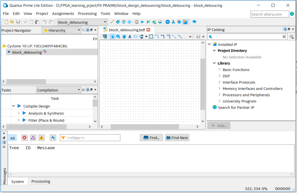
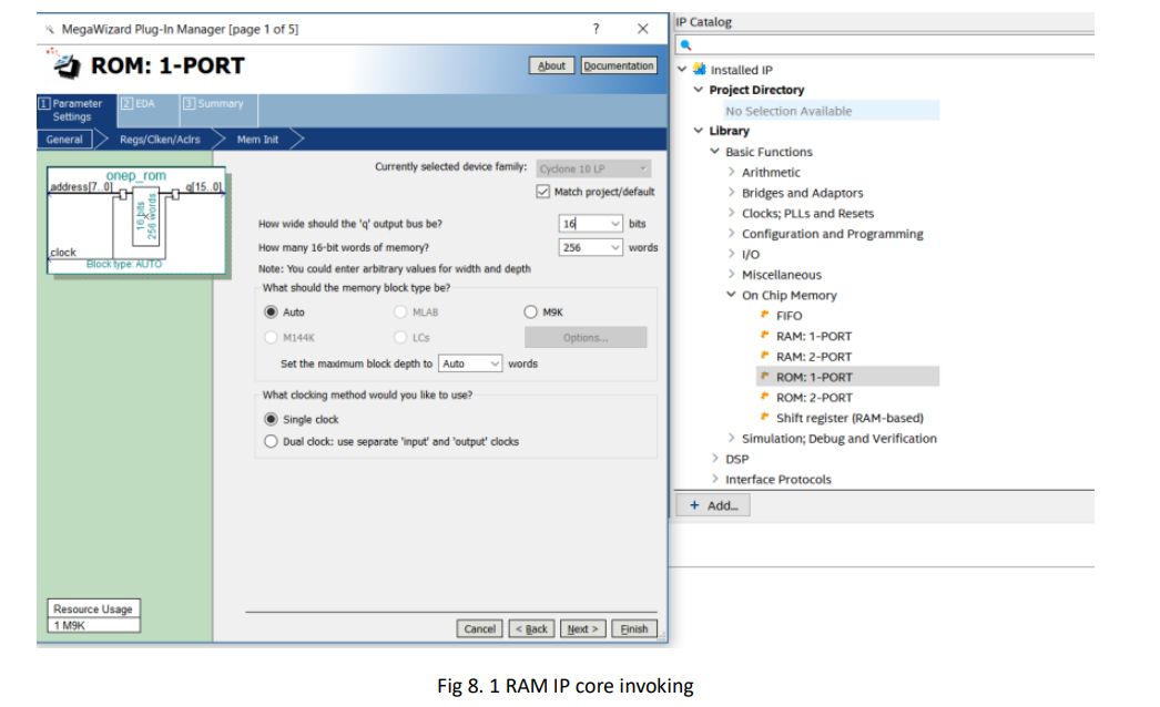
- In Installed IP, choose Library > Basic Function > On Chip Memory > ROM: 1-PORT, file type to be Verilog HDL. Choose 16 bits and 256 words for output. See Figure 8.1.
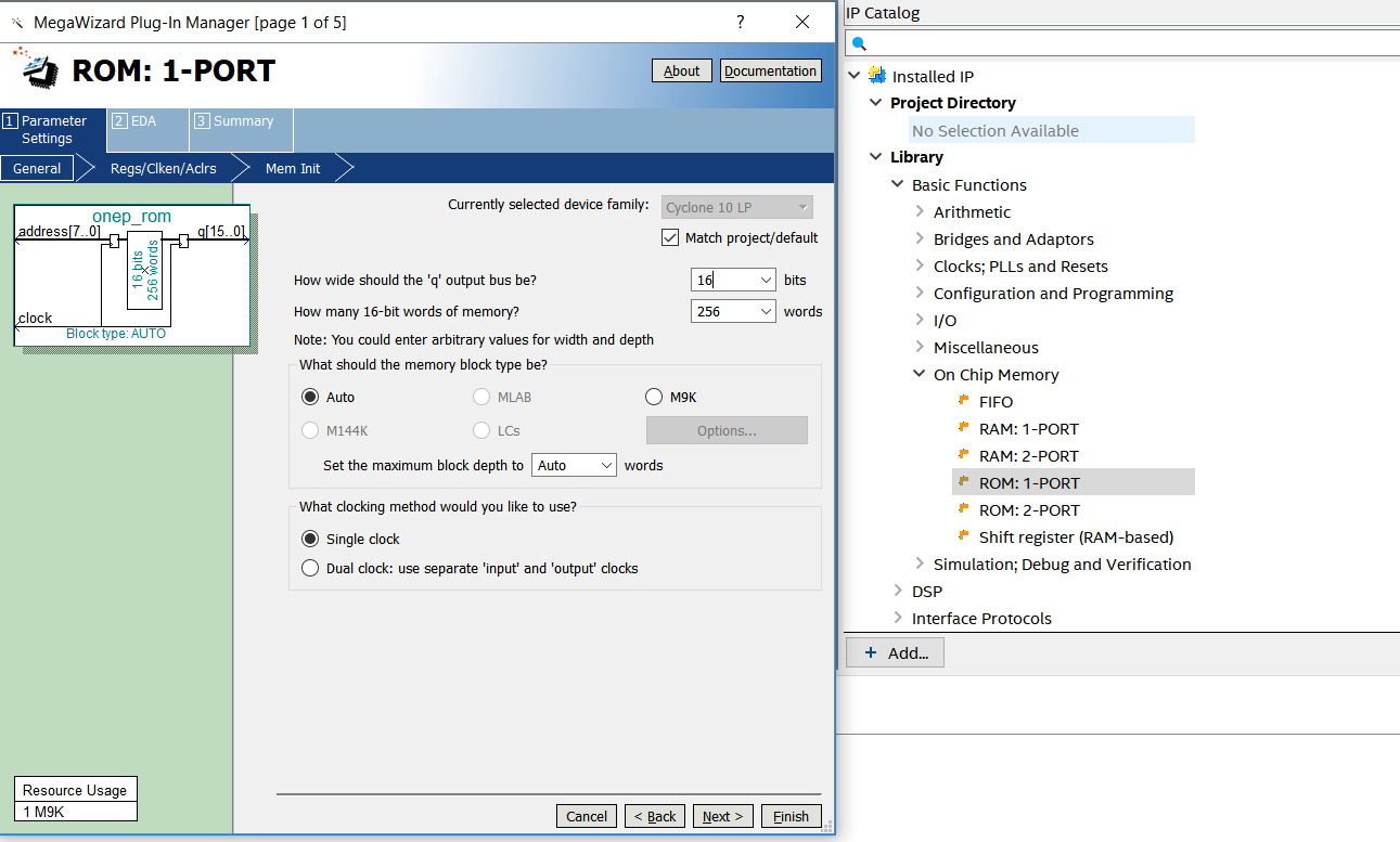
Figure 8.1 RAM IP core invoking
- According to the default setting, an initial ROM file in the location where red oval circles needs to be added. See Figure 8.2. In the figure, a *.mif file has already been added.
- Create a top level entity rom.mif
- Generate rom.mif file. Go to File > New > Memory Files > Memory Initialization File. See Figure 8.3.
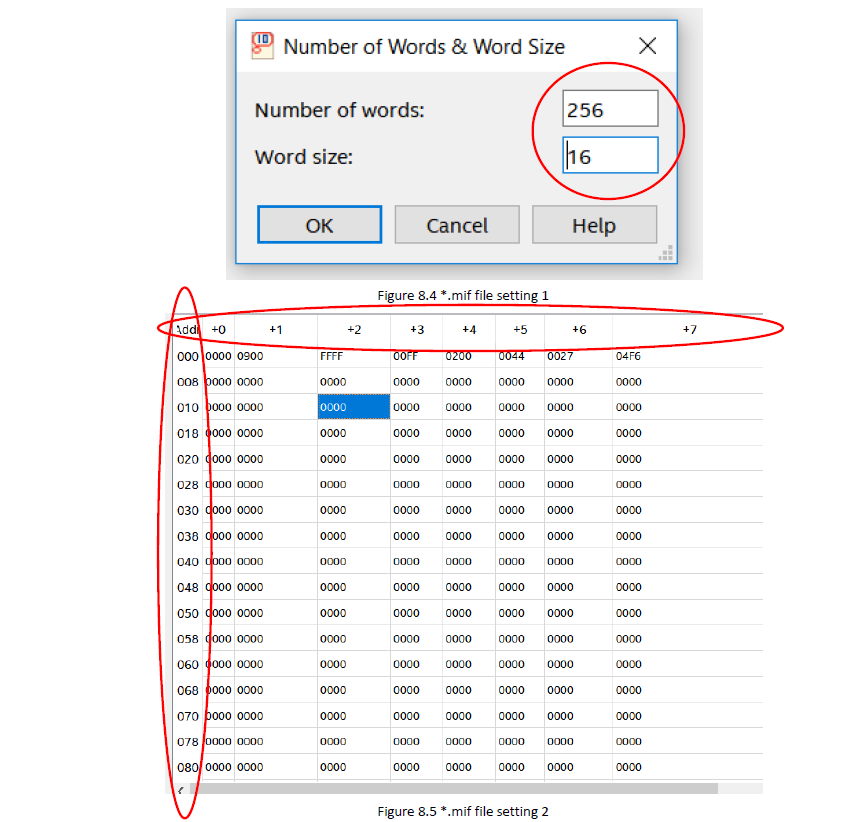
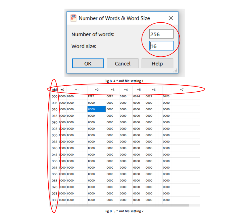
- In Figure 8.4, modify the Number of words and Word size.
- In Figure 8.5, in the address area, right click to input the data or change the display format, such as hexadecimal, octal, binary, unsigned, signed, etc
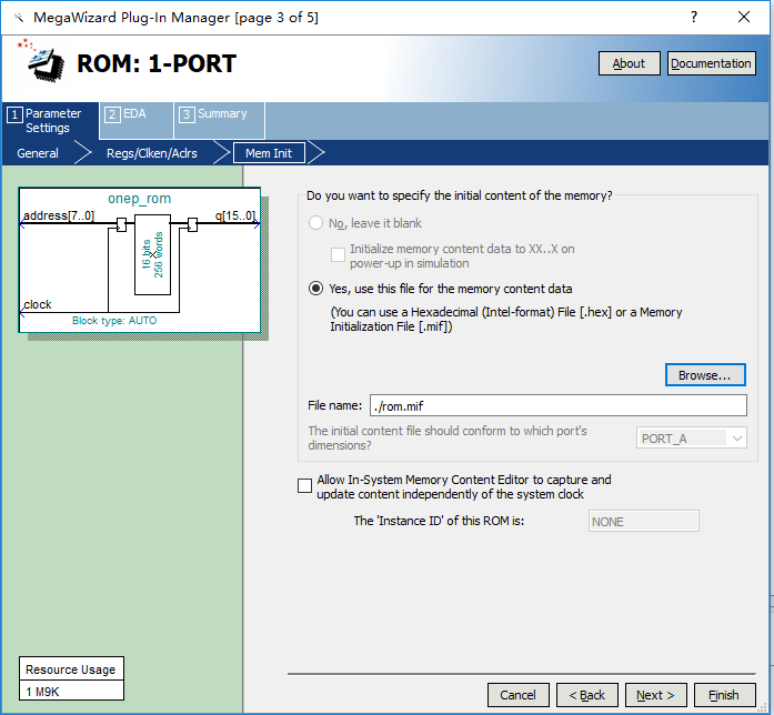
Figure 8.2 ROM setting
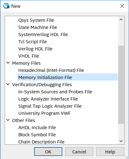
Figure 8.3 New *.mif file
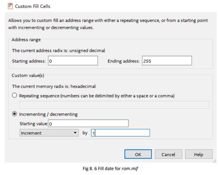
- After completing the ROM and IP’s setting, fill the data for rom.mif. For convenience of verification, store the same data as the address from the lower byte to higher byte in ascending form. Right click to select Custom Fill Cells. See Figure 8.6. The starting address is 0, ending at 255 (previous address setting depth is 256). The initial value is 0 and the step is 1.
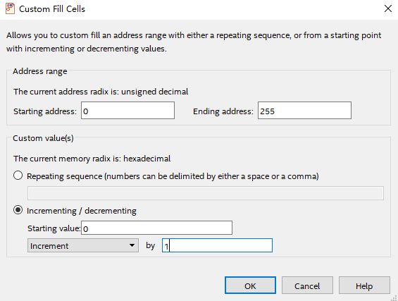
Figure 8.6 Fill date for rom.mif
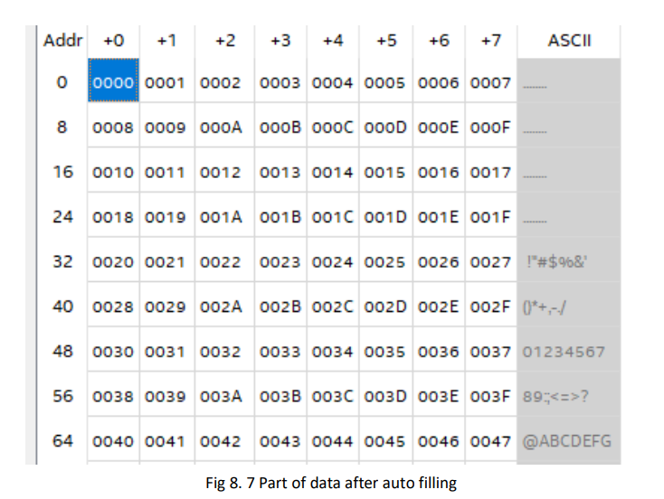
- After the setup, the system will fill in the data automatically. See Figure 8.7.
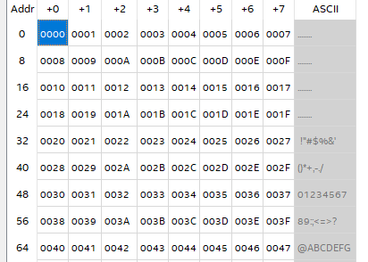
Figure 8.7 Part of data after auto filling
- Refer to the design of conversion from hexadecimal to BCD in Experiment 7, the data rom_q in the ROM is synchronized by the primary register and displayed on the segment display.
ROM instantiation:
reg	[15:0] rom_q_r;

always @ (posedge BCD_clk)
	rom_q_r<=rom_q;

HEX_BCD HEX_BCD_inst(
	.hex			    (rom_q_r),
	.ones			(ones),
	.tens			    (tens),
	.hundreds		(hundreds),
	.thousands		(thousands),
	.ten_thousands	(ten_thousands)
);
onep_rom  onep_rom_dut(
	.address		    (sw),
	.clock			(sys_clk),
	.q				(rom_q)
);
8.4 Experiment Verification
Pin assignments are consistent with Experiment 7. After the compilation is completed, the board is verified. As shown in Figure 8.8. When the DIP switch is 10010100, the decimal expression is 148, which means the contents of the 148th byte of the ROM is read, and the segment display will illustrate 148, which is consistent with the data deposited before.
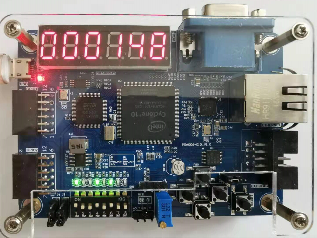
Figure 8.8 Experiment phenomenon
Experiment Summary and Reflection
- How to use the initial file of ROM to realize the decode, such as decoding and scanning the segment display.
- Write a *.mif file to generate sine, cosine wave, and other function generators.
- Comprehend application, combine the characteristic of ROM and PWM to form SPWM modulation waveform.
Old Version (2019)
8.1 Experiment Objective
-
Study the internal memory block of FPGA
-
Study the format of *.mif and how to edit *.mif file to configure the contents of ROM
-
Learn to use RAM, read and write RAM
8.2 Experiment Requirement
- Design 16 outputs ROM, address ranging 0-255
- Interface 8-bit switch input as ROM’s address
- Segment decoders display the contents of ROM and require conversion of hexadecimal to BCD output.
8.3 Experiment
8.3.1 Design Procedure
-
Build a new project named memory_rom
-
In Installed IP, choose Library > Basic Function > On Chip Memory > ROM: 1-PORT, file type to be Verilog HDL. Choose 16 bits and 256 words for output. See Fig 8. 1
RAM IP core invoking
Fig 8. 1 RAM IP core invoking
3. According to the default setting, you need to add an initial ROM file in the location where red oval circles. See Fig 8. 2. In the figure, a *.mif file has already been added. (Refer to the project files)
4. Create a top level entity rom.mif
a. Go to File > New > Memory Files > Memory Initialization File. See Fig 8. 3
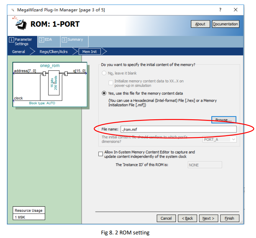
Fig 8. 2 ROM setting
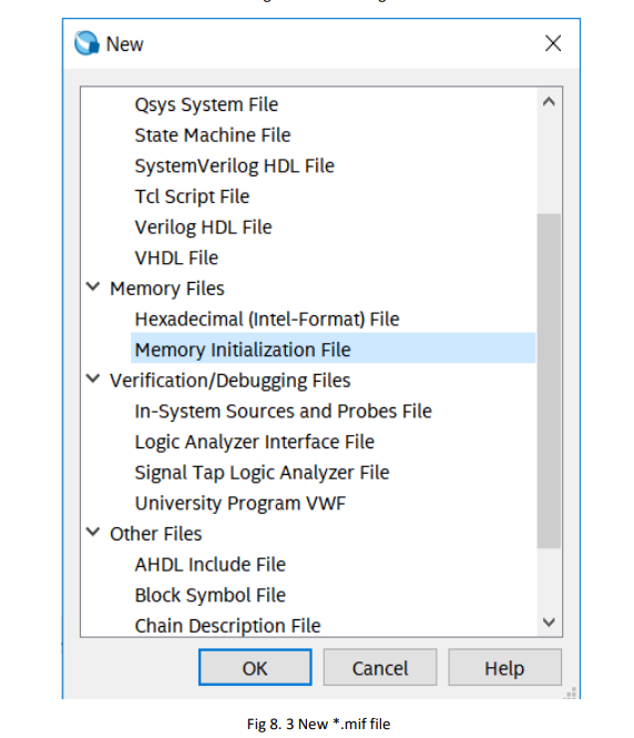
Fig 8. 3 New *.mif file
b. In Fig 8. 4, modify the Number of words and Word size.
c.In Fig 8. 5. In the address area, right click and you can input the data or change the display format, such as hexadecimal, octal, binary, unsigned, signed, etc.
-
-
After completing the ROM and IP’s setting, fill the data for rom.mif. For convenience of verification, store the same data as the address from the lower byte to higher byte in ascending form. Right click to select Custom Fill Cells. See Fig 8. 6. The starting address is 0, ending at 255 (previous address setting depth is 256). The initial value is 0 and the step is 1.
-
After the setup, the system will fill in the data automatically. See Fig 8. 7
Fill date for rom.mif
-
-
Refer to the design of conversion from hexadecimal to BCD in Experiment 7, the data rom_q in the ROM is synchronized by the primary register and displayed on the segment display.
ROM instantiation:reg [15:0] rom_q_r; always @ (posedge BCD_clk) rom_q_r<=rom_q; HEX_BCD HEX_BCD_inst( .hex (rom_q_r), .ones (ones), .tens (tens), .hundreds (hundreds), .thousands (thousands), .ten_thousands (ten_thousands) ); onep_rom onep_rom_dut( .address (sw), .clock (sys_clk), .q (rom_q) );
8.3.2 Board Verification
Compile, lock the pins, and verify the experiment downloading the program to the develop board.
Reflection:
- How to use the initial file of ROM to realize the decoding, such as decoding and scanning the segment decoders.
- Write a *.mif file to generate sine, cosine wave, and other function generators.
- Comprehend application, combine the characteristic of ROM and PWM to form SPWM modulation waveform.
-