LED_shifting , Frequency Divider Verilog HDL Code using the development software Quartus, FPGA pin assignment – FPGA Board Beginner Tutorial – FII-PRA006 Experiment 1
Experiment 1 LED shifting
1.1 Experiment Objective
- Practice using the development software Quartus, the building of new projects, and the use of system resources IP Core;
- Proficiency practice in the writing of Verilog HDL programs to develop a fine code writing style;
- Master the design of the frequency divider to realize the design of LED shifting;
- Mange FPGA pin assignment according to the schematics, and verify it though programming the development board;
- Observe and summarize the experiment result
1.2 Experiment Implement
- All LEDs are lit up when pressing self-defined reset button;
- After resetting, LEDs light from low to high (from right to left) in turn;
- Each LED light is on for 1 second;
- After the last left (highest position) LED is lit, the next time it returns to the first right (lowest position) LED, to create a light shifting loop;
1.3 Experiment
1.3.1 Introduction to LED
LED (Light-Emitting Diode), is characterized by low operating current, high reliability and long life. Up to now, there are many types of LED lights, as shown in Figure 1.1. The FII-PRA006 uses the LED lights in the red circle.
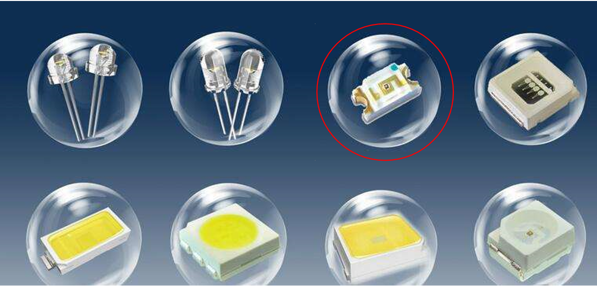
Figure 1.1 Different kinds of LEDs
1.3.2 Hardware Design
The physical picture of the onboard 8-bit LED is shown in Figure 1.2. The schematics of LED is shown in Figure 1.3 (In the red rectangular). The LED module of this experiment board adopts 8 common anode LEDs, which are connected with Vcc 3.3V through 270 R resistors, and the cathodes are grounded through the N-channel FET (In the green rectangular). The FET gate is grounded through a 4.7K resistor, and the FPGA is connected to the FET gate through the SW_LED terminal (In the blue rectangular). Therefore, when the FPGA is set to 1, the output is high. The FET is turned on, then the LED is turned on, and the LED is on.
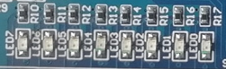
Figure 1.2 Physical picture of 8-bit LED
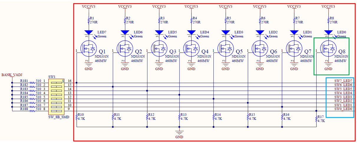
Figure 1.3 Schematics of LED
1.3.3 Program Design
1.3.3.1 System Block Diagram
See Figure 1.4 for the LED shifting system block diagram.
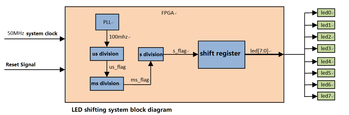
Figure 1.4 LED shifting system block diagram
1.3.3.2 Introduction to the program
Before writing a program, the development environment used and new project building are breifly introduced. Take the Quartus 18.1 version of the synthesizer as an example. The specific project establishment steps are shown in Figure 1.5 to 1.10.
- As shown in Figure 1.5, after opening Quartus, directly click New Project Wizard in the middle of the screen to create a new project, or click File to create a new project in the toolbar, or press Ctrl + N and follow the prompts to create a new project.
- As shown in Figure 1.6, select the correct project path. The project is named LED_shifting. It is recommended that the path is simple and easy to be found, which is convenient for later use and invoke.
- As shown in Figure 1.7, some files written in advance can be directly added, since it is a new project, click Next to perform the next step.
- As shown in Figure 1.8, select the correct FPGA chip model, the onboard chip model is 10CL006YE144C8G or 10CL010YE144C8G, select Cyclone 10 LP in the Family, select 144 in the Pin count, and select 8 in the Core speed grage. That helps narrow down the selection range and the target model can be found quickly.
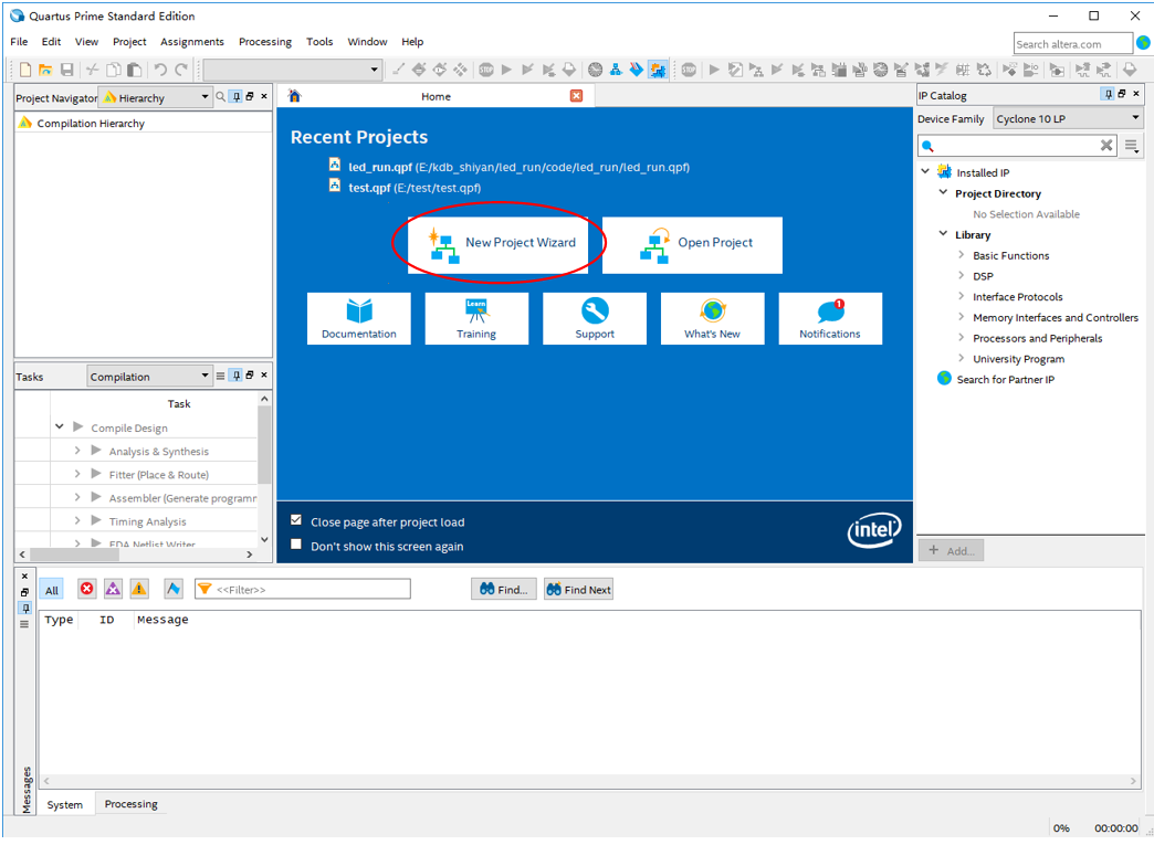
Figure 1.5 Quartus II 18.1 interface
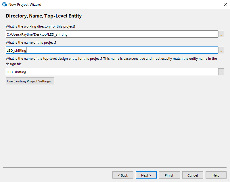
Figure 1.6 Path selection and naming of the project files
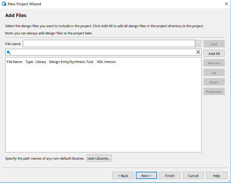
Figure 1.7 Add files
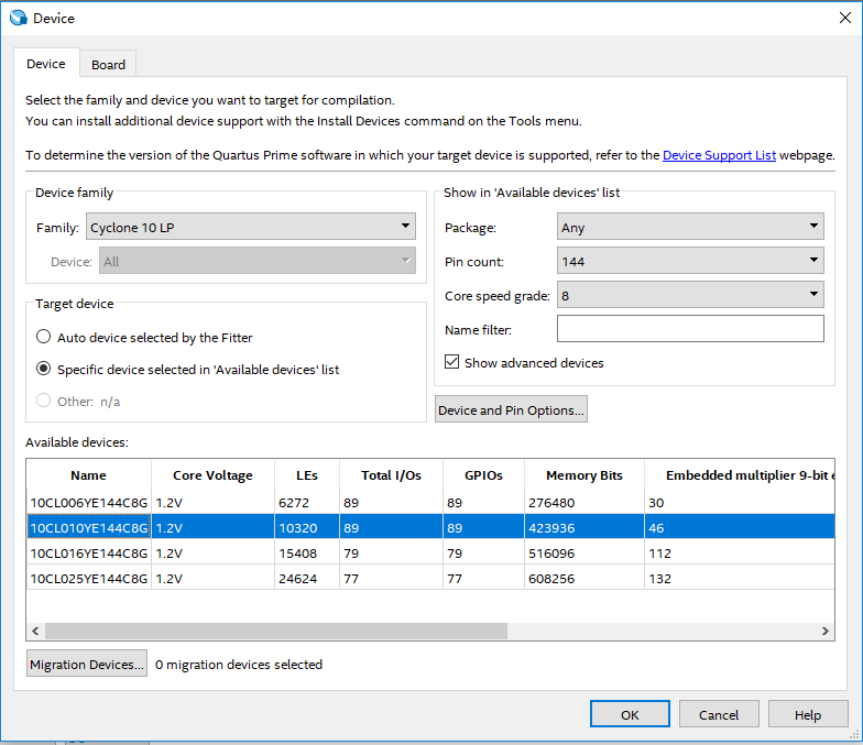
Figure 1.8 Device selection
- As shown in Figure 1.9, use the EDA tool that comes with Quartus.
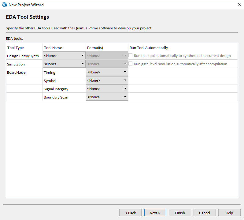
Figure 1.9 Selection of EDA tool
- Click Next to proceed to the next interface and select Finish to complete the project building.
- Click File > New or use the shortcut key Ctrl+N to pop up the dialog box shown in Figure 1.10, to create a program file (note: Verilog HDL File), and write the code. Pay attention to the consistency of the program name and project name, and save it in the correct path (folder).
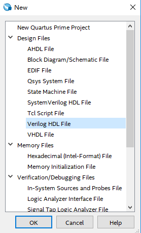
Figure 1.10 Start a new file (ii)
After the preparation is finished, starting to write the program, as described below.
The first step: the establishment of the main program framework (interface design)
module Led_shifting(

input rst,

input clk,

output reg [7:0] led

);

endmodule
The input signals of this experiment have 50MHz system clock clk, reset signal rst, and output signal led; 8 LEDs are defined by multi-bit width form of led [7:0], which reduces the code amount and facilitates code writing.
The second step: the invoke of IP Core and the establishment and use of PLL module
- See Figure 1.11, find ALTPLL in the IP catalog option bar on the right side of the main interface
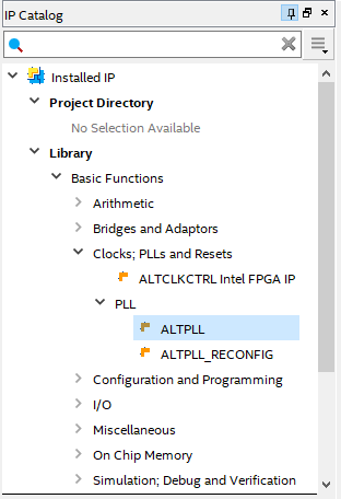
Figure 1.11 IP Catalog
- As shown in Figure 1.12, double-click ALTPLL and enter the name of the PLL module in the pop-up dialog box. The name given here is PLL1. Note that the selection type is Verilog language type.
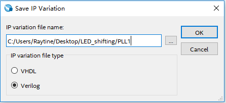
Figure 1.12 PLL naming
- As shown in Figure 1.13, after completing the previous step, the detailed setting interface is proceeded. Inclk0 is the input clock of the PLL, provided by the development board, which should be consistent with the system clock, set to 50MHz; PLL feedback path is set to normal mode. For advanced features involved, please use Intel reference file; PLL compensation output clock is c0; after the setting is completed, click Next.
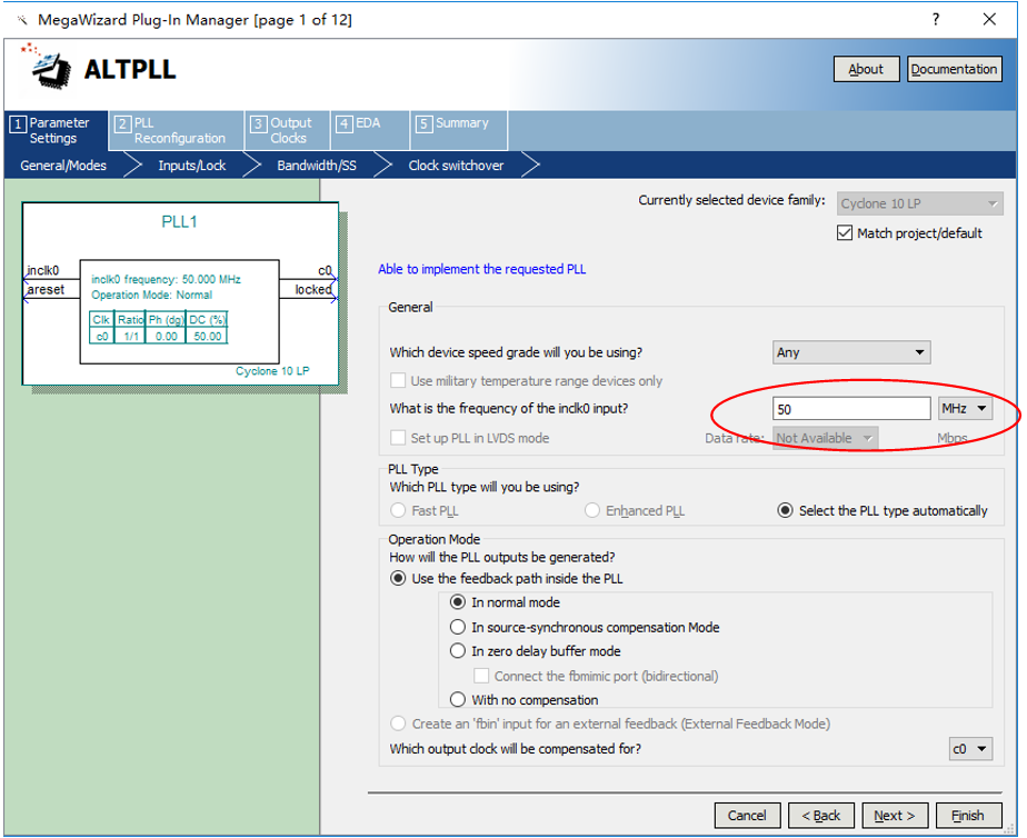
Figure 1.13 PLL setting 1 (input clock)
- As shown in Figure 1.14, it is the setting of PLL asynchronous reset (areset) control and capture lock (locked) status. This experiment can be set to default mode shown in the figure.
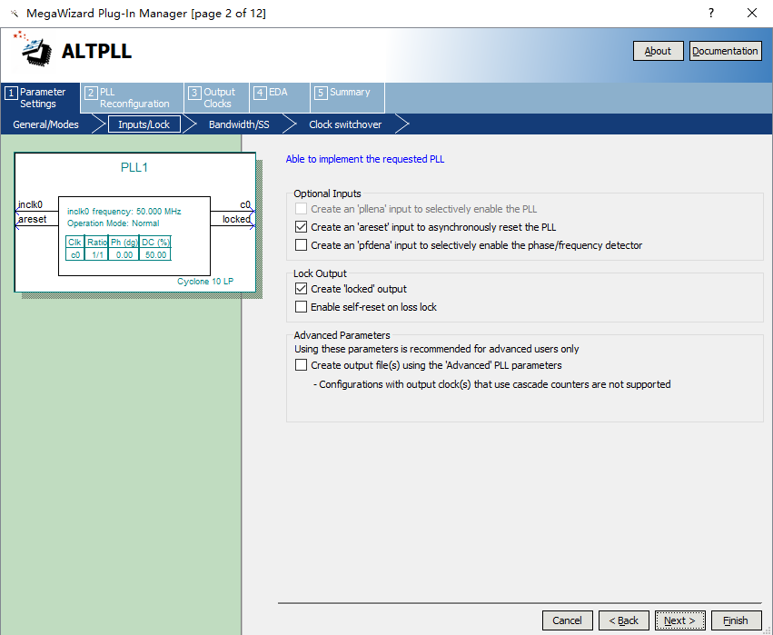
Figure 1.14 PLL setting 2
- Click Next in the next 3 steps. Default settings are used.
- As shown in Figure 1.15, it is the setting of the PLL output clock. It can output 5 different clocks clk c0~c4. This experiment only uses one, set clk c0, other defaults are not applicable.. Set the output frequency to 100 MHz, the phase shift is set to 0, and the duty cycle is set to 50%.
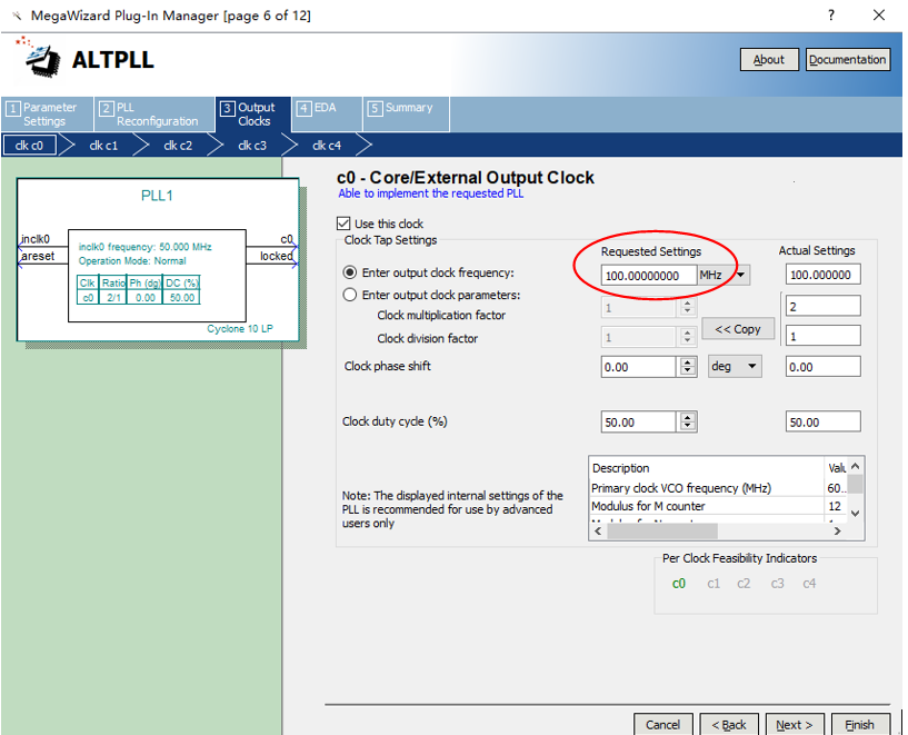
Figure 1.15 PLL setting 3 (output clock)
- Keep the EDA setting to be default
- As shown in Figure 1.16, the output file type setting selects *.bsf (used in the subsequent design of graphic symbols) files and *.v files. Others are set by default and click Finish to complete the settings.
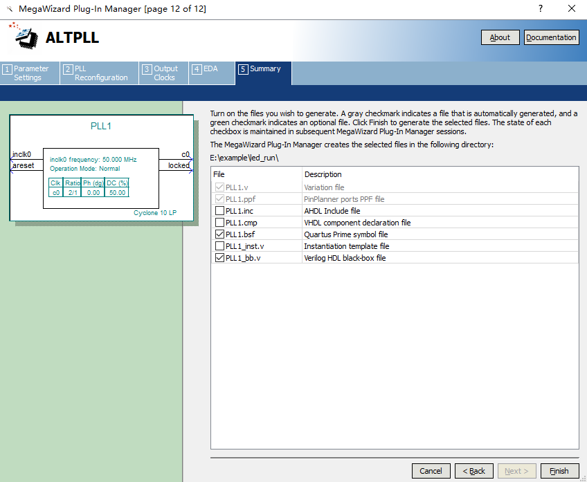
Figure 1.16 PLL setting 4 (output file type setting)
- As shown in Figure 1.17, select file in the Project Navigator type box of the project interface (the default is the project hierarchy)
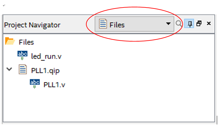
Figure 1.17 PLL1.v file location
- As shown in Figure 1.18, click PLL1.v. The main window will display the contents of the PLL, find the module name and port list, copy it to the top level entity, and instantiate it.
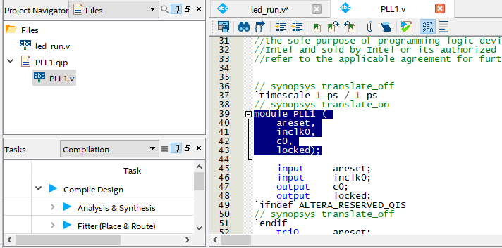
Figure 1.18 PLL1.v
When the system is powered on, the pll_locked signal has a value of 0 before the PLL is locked (stable operation), pll_locked is pulled high after the PLL is locked, and the clock signal sys_clk is output normally. The phase-locked loop is instantiated as follows:
wire sys_clk;

wire pll_locked;

PLL1 PLL1_inst

(

.areset (1'b0),

.inclk0 (clk),

.c0 (sys_clk),

.locked (pll_locked)

)
- Sys_rst is used as the reset signal of the frequency division part, and ext_rst is used as the reset signal of the LED shifting. Under the drive of the clock sys_clk, it is synchronously reset by the primary register.
reg           sys_rst;
reg           rxt_rst;
always @ (posedge sys_clk)
begin
    sys_rst <= !pll_locked;
    ext_rst <= rst;
end
The third step: the design of the frequency divider
100 MHz clock output by PLL is used as the system clock. The experiment requires the shifting speed of LEDs to be 1 second, thus frequency division is applied. The design is firstly obtained 1us by microsecond frequency division, then 1ms is obtained by millisecond frquency division, and finally 1s clock is achieved through second frequency division.
- Microsecond frequency division
reg    [6:0]  us_cnt;
reg          us_f;
always @ (posedge sys_clk)
begin
	if (sys_rst) begin
		us_cnt <= 0;
		us_f <= 1'b0;
	end
	else begin
		us_f <= 1'b0;
		if (us_cnt == 99) begin
			us_cnt <= 0;
			us_f <= 1'b1;
		end
		else
			us_cnt <= us_cnt + 1'b1;
	end
end
The 100 MHz clock has a period of 10ns, and 1us requires 100 clock cycles, that is, 100 10ns. Therefore, a microsecond counter us_cnt [6:0] and a microsecond pulse signal us_f are defined. The counter is cleared at reset. On each rising edge of the clock, the counter is incremented by one. When the counter is equal to 99, the period of 1us elapses, and the microsecond pulse signal us_f is pulled high. Thus, every 1us, this module will generate a pulse signal.
- Millisecond frequency divider
Similarly, 1ms is equal to 1000 1us, so a millisecond counter ms_cnt [9:0] and a microsecond pulse signal ms_f are defined.
reg    [9:0]  ms_cnt;
reg          ms_f;
always @ (posedge sys_clk)
begin
	if (sys_rst) begin
		ms_cnt <= 0;
		ms_f <= 1'b0;
	end
	else begin
		ms_f <= 1'b0;
		if (us_f) begin
			if (ms_cnt == 999) begin
				ms_cnt <= 0;
				ms_f <= 1'b1;
                       end
		else
				ms_cnt <= ms_cnt + 1’b1;
		end
	end
end
- Second frequency divider
Similarly, 1s is equal to 1000 1ms, so a second counter s_cnt [9:0] and one second pulse signal s_f are defined. When the three counters are simultaneously full, the time passes for 1 s and the second pulse signal is issued.
reg    [9:0]  s_cnt;
reg          s_f;
always @ (posedge sys_clk) begin
	if (sys_rst) begin
		s_cnt <= 0;
		s_f <= 1'b0;
	end
	else begin
		s_f <= 1'b0;
		if (ms_f) begin
			if (s_cnt == 999) begin
				s_cnt <=0;
				s_f <= 1'b1;
		end
		else
			s_cnt <= s_cnt + 1'b1;
		end
	end
end
The fourth step: the design of the shifting LED
When resetting, 8 LEDs are all on, so the output led is 8’hff. The LEDs need to light one by one, so the lowest LED is lit first. At this time, the led value is 8’b0000_0001. When the second pulse signal arrives, the next LED is illuminated, and the value of led is 8’b0000_0010.It can be seen that as long as the high level of “1” is shifted to the left, it can be realized by bit splicing, that is, led <= {led[6:0], led[7]}.
always @ (posedge sys_clk)
begin
	if (ext_rst)
		led <= 8'hff;
	else begin
		if (led == 8'hff)
			led <= 8'b0000_0001;
		else if (s_f)
			led <= {led[6:0], led[7]};
	end
end
1.4 Experiment Verification
1.4.1 Some Preparation Before Verification
 Figure 1.19 Introduction to some functions
As shown in Figure 1.19, after the program is written, analysis and synthesis is required to check for errors. Click the synthesis icon to complete, or use the shortcut key Ctrl+K, the pin assignment is to bind each signal to the FPGA pin, the compilation is to generate the programming file for the development board and check the error again. Click the programmer icon, and follow the instructions to program the development board. Click on the synthesis icon, Quartus will automatically generate a report after that, as shown in Figure 1.20. The details of the report are not described here.
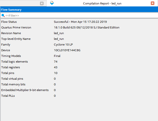
Figure 1.20 Compilation report
Check and modify to no error before board verification. Do the pin assignment before actually programming the board. See Table 1.1 for the pin assignment.
Table 1.1 LED pin mapping
| Signal Name | Network Label | FPGA Pin | Port Description |
| clk | C10_50MCLK | 91 | Input clock |
| rst | KEY3 | 10 | Reset button |
| led[7] | SW7_LED7 | 77 | LED 7 |
| led[6] | SW6_LED6 | 76 | LED 6 |
| led[5] | SW5_LED5 | 75 | LED 5 |
| led[4] | SW4_LED4 | 74 | LED 4 |
| led[3] | SW3_LED3 | 87 | LED 3 |
| led[2] | SW2_LED2 | 86 | LED 2 |
| led[1] | SW1_LED1 | 83 | LED 1 |
| led[0] | SW0_LED0 | 80 | LED 0 |
Click the pin assignment icon to open the pin assignment window, as shown in Figure 1.21. Double-click the location column corresponding to each pin, directly enter the pin number, or click the drop-down button to find the corresponding pin, but the latter is relatively slow.
It should be noted that the I/O standard column in Figure 1.21, the content shown is the voltage standard of each I/O port, determined by the BANK voltage in the schematics and the design requirements. In this experiment, the I/O voltage should be selected as 3.3V. Double-click the I/O standard column and click the pull-down button, as shown in Figure 1.22, select the right voltage standard.
The default voltage standard can be set in advance when selecting the chip model. Click Device and Pin Options -> Voltage -> Default I/O standard in Figure 1.8 to set it.
The pin assignment is complete, as shown in Figure 1.23. Then click on the compilation.
After completion, program the development board.
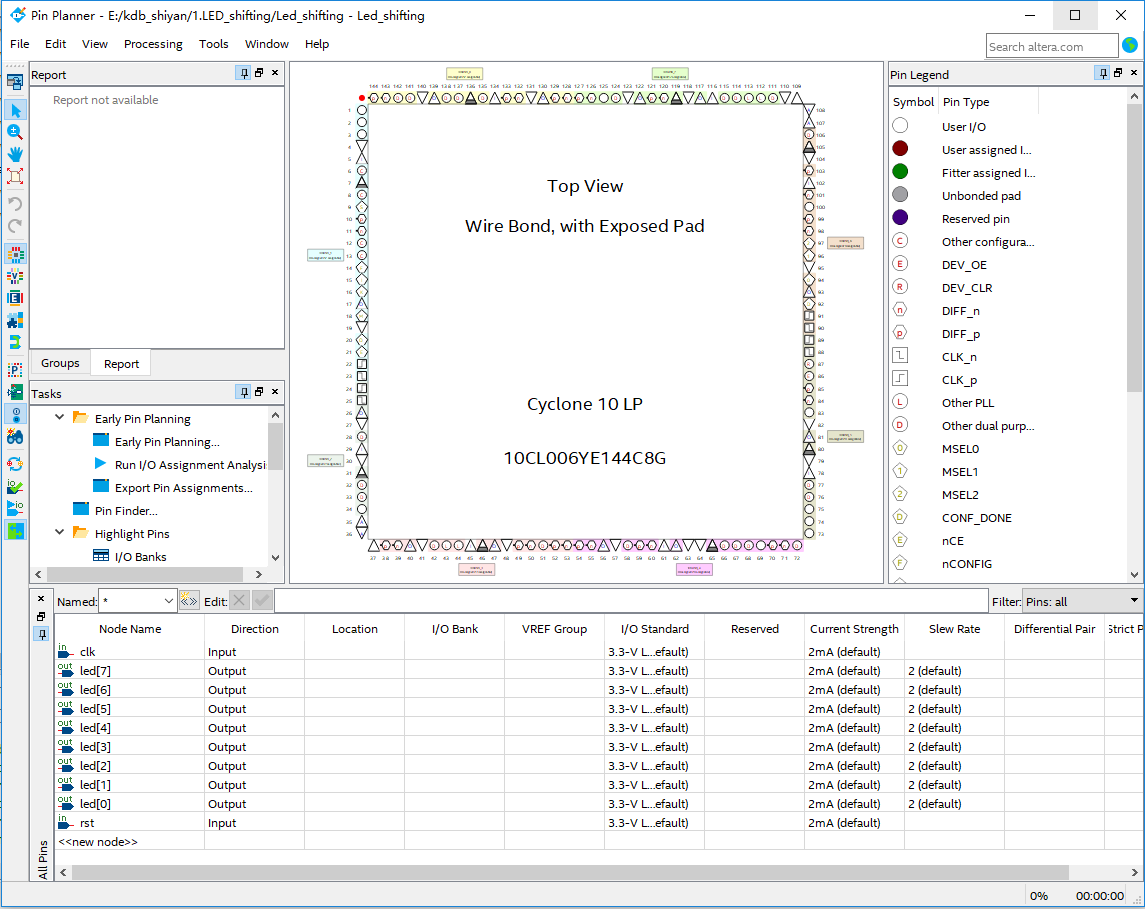
Figure 1.21 Pin assignment window
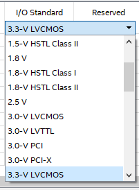
Figure 1.22 I/O voltage selection
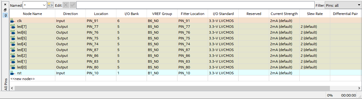
Figure 1.23 Pin assignment finished
1.4.2 Method and Steps to Program the Board
Before programming the board, some settings should be made for the Quartus. For details, please refer to the “Intel FPGA Download Cable II User Guide” for reference. After the settings according to the instructions, click programmer icon to open the download window, as shown in Figure 1.24.
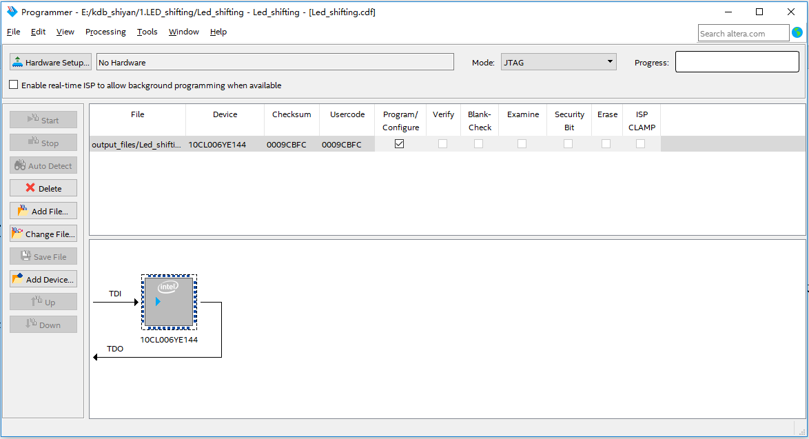
Figure 1.24 Program windows
After connecting the development board to the host computer, click on Hardware Setup and select development board, as shown in Figure 1.25.
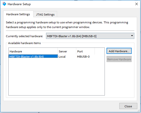
Figure 1.25 Hardware setup
Click Start to program the board, as shown in Figure 1.26, Progress shows 100% (Successful), that is, the download is completed.
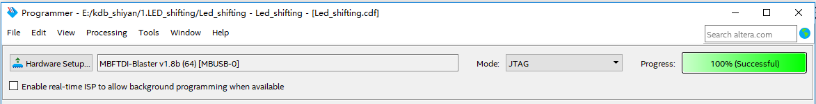
Figure 1.26 Programmed successfully
See Figure 1.27, the LEDs light one by one from low to high and the interval is one second.
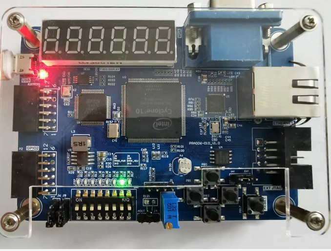
Figure 1.27 Experiment phenomenon