Xilinx Risc-V Board Tutorial : Hexadecimal Number to BCD Code Conversion and Application – FII-PRX100 FPGA Board Experiment 8
Experiment 8 Hexadecimal Number to BCD Code Conversion and Application
1.Experiment Objective
-
- Since the hexadecimal display is not intuitive, decimal display is more widely used in real life.
- Human eye recognition is relatively slow, so the display from hexadecimal to decimal does not need to be too fast. Generally, there are two methods
- Countdown method: Under the control of the synchronous clock, the hexadecimal number is decremented by 1 until it is reduced to 0. At the same time, the appropriate BCD code decimal counter is designed to increment. When the hexadecimal number is reduced to 0, the BCD counter just gets with the same value to display.
- Bitwise operations (specifically, shift bits and plus 3 here). The implementation is as follows:
- Set the maximum decimal value of the expression. Suppose you want to convert the 16-digit binary value (4-digit hexadecimal) to decimal. The maximum value can be expressed as 65535. First define five four-digit binary units: ten thousand, thousand, hundred, ten, and one to accommodate calculation results
- Shift the hexadecimal number by one to the left, and put the removed part into the defined variable, and judge whether the units of ten thousand, thousand, hundred, ten, and one are greater than or equal to 5, and if so, add the corresponding bit to 3 until the 16-bit shift is completed, and the corresponding result is obtained.
Note: Do not add 3 when moving to the last digit, put the operation result directly
-
-
-
- The Principle of hexadecimal number to BCD number conversion
-
-
Suppose ABCD is a 4-digit binary number (possibly ones, 10 or 100 bits, etc.), adjusts it to BCD code. Since the entire calculation is implemented in successive shifts, ABCDE is obtained after shifting one bit (E is from low displacement and its value is either 0 or 1). At this time, it should be judged whether the value is greater than or equal to 10. If so, the value is increased by 6 to adjust it to within 10, and the carry is shifted to the upper 4-bit BCD code. Here, the pre-movement adjustment is used to first determine whether ABCD is greater than or equal to 5 (half of 10), and if it is greater than 5, add 3 (half of 6) and then shift.
For example, ABCD = 0110 (decimal 6)
- After shifting it becomes 1100 (12), greater than 1001 (decimal 9)
- By plus 0110 (decimal 6), ABCD = 0010, carry position is 1, the result is expressed as decimal
- Use pre-shift processing, ABCD = 0110 (6), greater than 5, plus 3
- ABCD=1001(9), shift left by one
- ABCD=0010, the shifted shift is the lowest bit of the high four-bit BCD.
- Since the shifted bit is 1, ABCD = 0010(2), the result is also 12 in decimal
- The two results are the same
- Firstly, make a judgement, and then add 3 and shift. If there are multiple BCD codes at the same time, then multiple BCD numbers all must first determine whether need to add 2 and then shift.
- The first way is relatively easy. Here, the second method is mainly introduced.
Example 1:
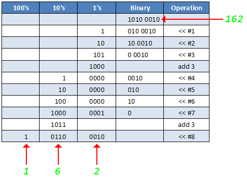
Fig 8. 1 Binary to decimal
Example 2:
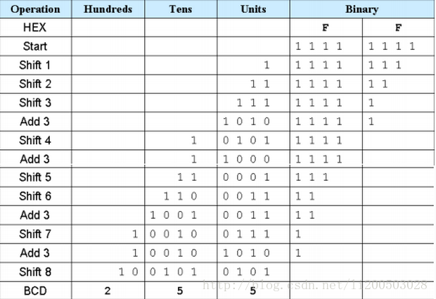
Fig 8. 2 Hex to BCD
-
- Write a Verilog HDL to convert 16-bit binary to BCD. (You can find reference in the project folder, HEX_BCD.v
| `timescale 10ns/1ns
module HEX_BCD ( input [15:0] hex, output reg[3:0] ones=0, output reg[3:0] tens=0, output reg[3:0] hundreds=0, output reg[3:0] thousands=0, output reg[3:0] ten_thousands=0 ); reg [15:0] hex_reg; integer i; always@(*) begin hex_reg =hex; Ones =0; Tens =0; Hundreds =0; Thousands =0; ten_thousands=0;
for (i=15;i>=0;i=i-1)begin if(ten_thousands>=5) ten_thousands=ten_thousands+3;
if(thousands>=5) thousands=thousands+3;
if(hundreds>=5) hundreds=hundreds+3;
if(tens>=5) tens=tens+3;
if(ones>=5) ones=ones+3;
ten_thousands =ten_thousands<< 1;//Left shift operation ten_thousands[0]=thousands[3]; thousands =thousands<<1; thousands[0]=hundreds[3]; hundreds=hundreds<<1; hundreds[0]=tens[3]; tens=tens<<1; tens[0]=ones[3]; ones=ones<<1; ones[0]=hex_reg[15]; hex_reg={hex_reg[14:0],1’b0}; end end endmodule |
-
- Modelsim simulation
- Refer to last experiment for setting Modelsim
- Simulation result shown in Fig 8. 3.
- Modelsim simulation
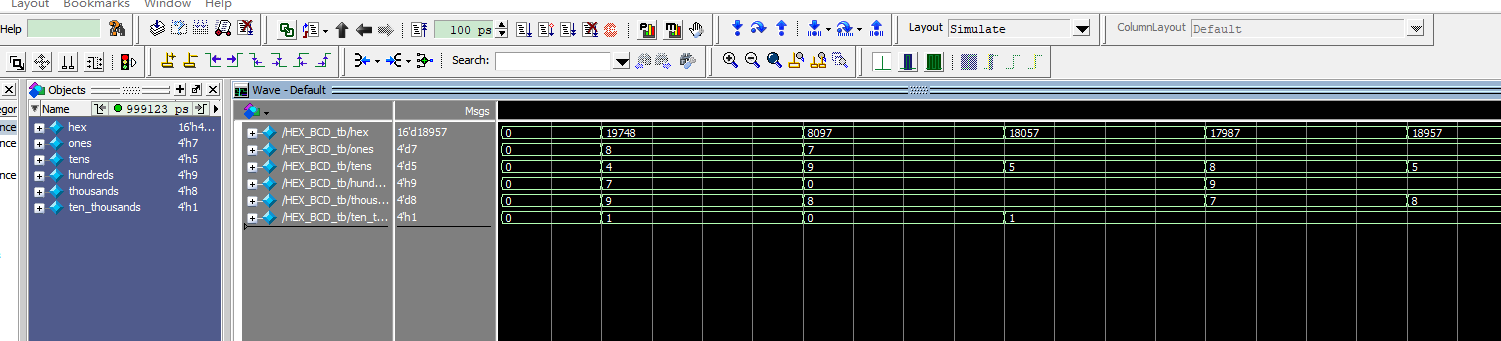
Fig 8. 3 Simulation result for Hex to BCD
-
- Remark
The assignment marks for the examples above are “=” instead of “<=”. Why?
Since the whole program is designed to be combinational logic, when invoking the modules, the other modules should be synchronized the timing.
2.Application of Hexadecimal Number to BCD Number Conversion
- Continue to complete the multiplier of experiment 7 and display the result in segment decoders in decimal. The code is as follows:
| module mult_sim(
input rst, input inclk, input [7:0] sw, output reg[6:0] seven_sega, output reg[5:0] scan ); wire [15:0] mult_res; wire sys_clk; wire sys_rst; wire us_f; wire ms_f; wire s_f; reg [7:0] count; reg [3:0] counta; reg [6:0] seven_seg_ra; wire [3:0] ones; wire [3:0] tens; wire [3:0] hundreds; wire [3:0] thousands; wire [3:0] ten_thousands; reg [3:0] ones_r; reg [3:0] tens_r; reg [3:0] hundreds_r; reg [3:0] thousands_r; reg [3:0] ten_thousands_r; always@(posedge sys_clk) if(sys_rst) begin count <=0; ones_r <=0; tens_r <=0; hundreds_r<=0; thousands_r<=0; ten_thousands_r<=0; end else if(s_f) begin count<=count+1; ones_r <=ones; tens_r <=tens; hundreds_r<=hundreds; thousands_r<=thousands; ten_thousands_r<=ten_thousands; end reg ext_rst; always@(posedge sys_clk) ext_rst<=rst; reg [2:0] scan_st;
always@(posedge sys_clk) if(!ext_rst) begin scan<=6’b11_1111; counta<=4’b0; scan_st<=0; end else case(scan_st) 0:begin scan<=6’b11_1110; counta<=ones_r; if(ms_f) scan_st<=1; end 1:begin scan<=6’b11_1101; counta<=tens_r; if(ms_f) scan_st<=2; end 2:begin scan<=6’b11_1011; counta<=hundreds_r; if(ms_f) scan_st<=3; end 3:begin scan<=6’b11_0111; counta<=thousands_r; if(ms_f) scan_st<=4; end 4:begin scan<=6’b10_1111; counta<=ten_thousands_r; if(ms_f) scan_st<=5; end 5:begin scan<=6’b01_1111; counta<=0; if(ms_f) scan_st<=0; end default:scan_st<=0; endcase
always@(*) case(counta) 0:seven_seg_ra<=7’b100_0000; 1:seven_seg_ra<=7’b111_1001; 2:seven_seg_ra<=7’b010_0100; 3:seven_seg_ra<=7’b011_0000; 4:seven_seg_ra<=7’b001_1001; 5:seven_seg_ra<=7’b001_0010; 6:seven_seg_ra<=7’b000_0010; 7:seven_seg_ra<=7’b111_1000; 8:seven_seg_ra<=7’b000_0000; 9:seven_seg_ra<=7’b001_0000; default:seven_seg_ra<=7’b100_0000; endcase always@(posedge sys_clk) seven_sega<=seven_seg_ra;
lpm_mult8x8 lpm_mult8x8_inst ( .CLK(inclk), // input wire CLK .A(sw), // input wire [7 : 0] A .B(count), // input wire [7 : 0] B .P(mult_res) // output wire [15 : 0] P ); pll_sys_rst pll_sys_rst_inst ( .clk_in (inclk), .sys_clk (sys_clk), .sys_rst (sys_rst), .BCD_clk ( ) ); us_ms_s_div us_ms_s_div_inst ( .sys_rst (sys_rst), .sys_clk (sys_clk), .us_f (us_f), .ms_f (ms_f), .s_f (s_f) ); HEX_BCD HEX_BCD_inst ( .hex (mult_res), .ones (ones), .tens (tens), .hundreds (hundreds), .thousands (thousands), .ten_thousands (ten_thousands) ); endmodule |
- After completing the implementation process, click Open Implementation Design as shown in Fig 8. 4. Observe the Report Timing Summary and view the circuit timing report.
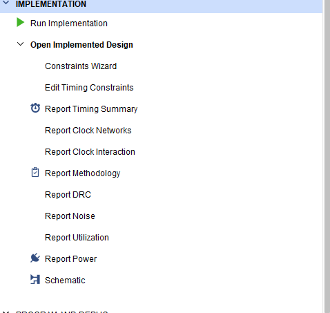
Fig 8. 4 Timing report check
The result is shown in Fig 8. 5.
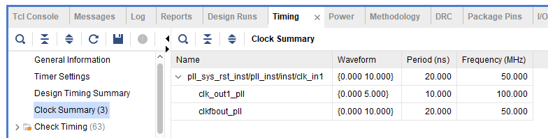
Fig 8. 5 Timing report
It satisfies the timing requirement.
- Pin assignment
| Signal Name | Port Description | Network Label | FPGA Pin |
| inclk | System clock, 50 MHz | C10_50MCLK | U22 |
| rst | Reset, high by default | KEY1 | M4 |
| seven_sega[0] | Segment a | SEG_PA | K26 |
| seven_sega[1] | Segment b | SEG_PB | M20 |
| seven_sega[2] | Segment c | SEG_PC | L20 |
| seven_sega[3] | Segment d | SEG_PD | N21 |
| seven_sega[4] | Segment e | SEG_PE | N22 |
| seven_sega[5] | Segment f | SEG_PF | P21 |
| seven_sega[6] | Segment g | SEG_PG | P23 |
| seven_sega[7] | Segment h | SEG_DP | P24 |
| scan[0] | Segment 6 | SEG_3V3_D5 | T24 |
| scan[1] | Segment 5 | SEG_3V3_D4 | R25 |
| scan[2] | Segment 4 | SEG_3V3_D3 | K25 |
| scan[3] | Segment 3 | SEG_3V3_D2 | N18 |
| scan[4] | Segment 2 | SEG_3V3_D1 | R18 |
| scan[5] | Segment 1 | SEG_3V3_D0 | R6 |
| sw[0] | Swicth input | GPIO_DIP_SW0 | N8 |
| sw[1] | Swicth input | GPIO_DIP_SW1 | M5 |
| sw[2] | Swicth input | GPIO_DIP_SW2 | P4 |
| sw[3] | Swicth input | GPIO_DIP_SW3 | N4 |
| sw[4] | Swicth input | GPIO_DIP_SW4 | U6 |
| sw[5] | Swicth input | GPIO_DIP_SW5 | U5 |
| sw[6] | Swicth input | GPIO_DIP_SW6 | R8 |
| sw[7] | Swicth input | GPIO_DIP_SW7 | P8 |
- Compile, and download the program to the board. The test result is shown below:
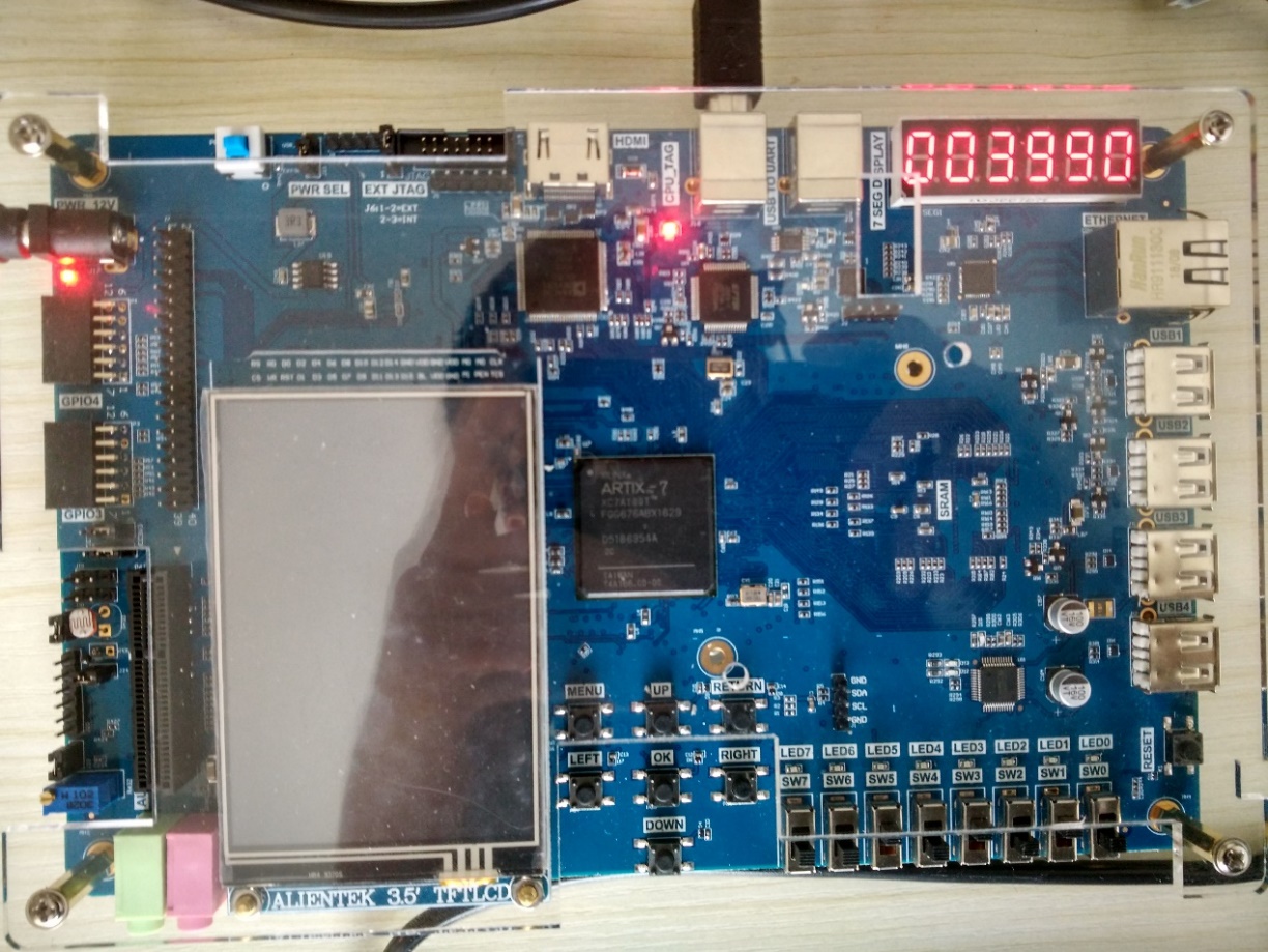
Fig 8. 6 Hex to BCD result
3.Experiment Reflection
-
- How to implement BCD using more than 16bits binarynumbers
- How to handle an asychrounus clock
- Learn how to design circuits that meet timing requirements based on actual needs