
FPGA Board for beginner – FII-PRA006/010 Hardware Reference Guide
V1.2
FII-PRA006/010 Hardware Reference Guide
Version Control
| Version | Date | Description |
| V1.0 | 06/25/2019 | Initial Release |
| V1.1 | 07/15/2019 | Add Description About PCF8591 |
| V1.2 | 07/19/2019 | Add Description About Oscillator and IIC |
Copyright Notice:
© 2019 Fraser Innovation Inc ALL RIGHTS RESERVED
Without written permission of Fraser Innovation Inc, no unit or individual may extract or modify part of or all the contents of this manual. Offenders will be held liable for their legal responsibility.
Thank you for purchasing the FPGA development board. Please read the manual carefully before using the product and make sure that you know how to use the product correctly. Improper operation may damage the development board. This manual is constantly updated, and it is recommended that you download the latest version when using.
Official Shopping Website:
Contents
7)Gigabit Ethernet Interface 22
9)AD/DA Thermistor, Photoresistor and Potentiometer 26
12)FLASH Configuration Chip 32
Fraser Innovation Inc develops FII-PRA006/010 based on Intel Cyclone10 development board. It was initial released in 2019. The model is PRA006/010. Although it is designed for FPGA beginners, this development board has been spent a lot on the schematics design, PCB design, and function creation. It can be described as “simple but powerful”.
PRA006/010 Full View Picture
Introduction
This development board uses Intel’s Cyclone10 series chip, model 10CL006YE144C8G or 10CL010YE144C8G.
The Cyclone10 series is Intel’s latest generation of FPGAs for the data torrent of the future and the rapidly growing IoT application market. This series provides fast, power-saving processing and is suitable for automotive, industrial automation, professional audio and visual systems and a variety of applications. Compared to previous generations of Cyclone FPGAs, the 10 Series saves more power while delivering twice the performance.
PRA006/010 system block diagram:
FPGA
Cyclone10
VGA
Gigabit Ethernet
JTAG
6 Digit 7-segment Decoders
4 Push Buttons
Reset
Potentiometer
Photoresistor
FLASH
128Mbit
8 DIP Switches
8 LEDs
EEPROM
AT24C02
(Back)
50M Oscillator
Thermistor
GPIO Interface
USB to Serial Chip
AD/DA
(Back)
USB Power Supply and Download Interface
GPIO Interface
External I2C Interface
External A/D Interface
Figure 1.1 PRA006/100 System Block Diagram
Ethernet Chip RTL8211E
Chip resource:
Figure 1.2 Chip Resource
Other parameters:
Working temperature:0~85℃
Core voltage:1.15~1.25V(Recommended voltage 1.2V)
Hardware resources:
- The USB interface provides power interface, program download, and can be used as a USB to serial port. Achieved the function of one wire to complete the power supply, download functions, and serial communication;
- A 50 MHz oscillator, a 32.768 kHz oscillator, provides a stable clock source for the development board;
- 6-digit common anode 7-segment LED display, through dynamic scanning to achieve data display;
- 1-channel VGA interface to display colorful pictures or camera video;
- 1 EEPROM chip with I2C interface, model AT24C02;
- 1 adaptive 10M/100M/Gigabit Ethernet interface;
- 5 push buttons, 4 for programmable buttons, 1 for reset button;
- 1 photoresistor, through which it can simulate light control; 1 thermistor, which can collect temperature or analog temperature alarm function; 1 potentiometer, which can simulate voltage change etc;
- 1 PCF8591 AD/DA conversion chip;
- On-board 50MHz oscillator, through which provides a stable clock signal to the development board;
- 8-digit DIP switch;
- 8-bit LED;
- 1-piece 128Mbit Flash chip;
- 2 GPIO external signal expansion interfaces;
- One JTAG interface, which makes PRA006/010 a full-featured JTAG adapter, which can download programs for FPGAs from Intel, Xilinx and other vendors;
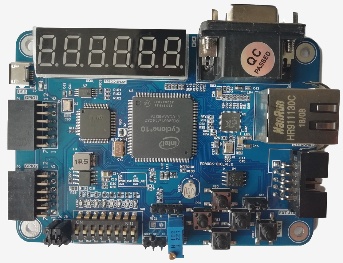
Before using the development board, it is necessary to check whether the power supply and jtag mode jumpers are correct. J9 is the selection jumper for either internal or external program download (when this development board is used as the downloader). For the internal download program, connect “INT”. When using it as a downloader, connect “EXT”. J6 is used to select FPGA BANK power supply, generally 3.3V and 5V . And J8 will be used to select bank IO voltage. Its jumper description is silk screen printed on the development board, as shown below.
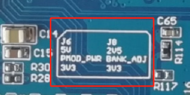
Figure 1.3 Power Selection Jumper
Basic Features
As mentioned above, this development board FPGA model is 10CL006YE144C8G (PRA010 uses 10CL010YE144C8G), which is Intel’s latest generation of low-power high-performance FPGA.
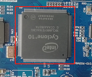
Figure 2.1 FPGA Physical Picture
It is a micro USB interface onboard that integrates power supply, program download and serial communication functions.
Figure 2.2 USB Interface Physical Picture
By the way to mention the power supply circuit of the development board and the power supply of the FPGA. When the USB cable (sold with the board as a set) is connected to the development board and the computer’s USB port, the development board will work through the 5V power supply provided by the computer’s USB interface, but instead of directly using the 5V level, the 5V voltage will be converted by the conversion chip to the required voltages such as 1.2V, 2.5V, 3.3V. See Figure 2.3 for the schematics of the USB interface and power conversion chip.
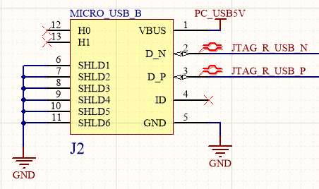
Figure 2.3 Schematics of Micro USB
The external input power PC_USB5V is connected to the 5V level network of the development board, and then converted from the 5V level network to 1.2V (FPGA core voltage) required by the FPGA, 2.5V or 3.3V. Both 2.5V and 3.3V are FPGA BANK voltages. The two voltages are provided to accommodate various external signal level standards. The conversion circuit is shown below.
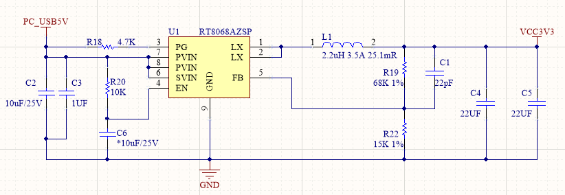
Figure 2.4 Schematics of 3.3V Power Supply
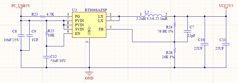
Figure 2.5 Schematics of 2.5V Power Supply
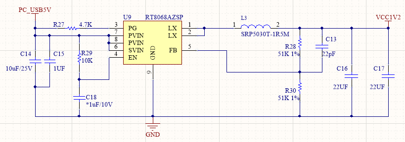
Figure 2.6 Schematics of 1.2V Power Supply
If we look at the power supply of the FPGA, we can see these kinds of voltages:
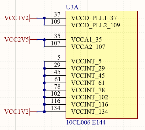
Figure 2.7 Pins of FPGA Power Supply
In Figure 2.7, VCCD_PLL1_37, VCCD_PLL2_109 are the power supply pins of the FPGA phase-locked loop(PLL), and the following numbers 37, 109 are their pin numbers on the FPGA. VCCINT is the core voltage of the FPGA (the other power supply parts of the FPGA are not listed, please refer to the attached schematics for details).
As a communication serial port, its D_N and D_P pins are connected to the FT2232HL chip (this is a chip specially used as a USB to UART), which is processed by the FT2232HL and then connected to the FPGA and JTAG ports.
| Signal Name | FPGA Pin |
| JTAG_RXD | 143 |
| JTAG_TXD | 144 |
One on-board oscillators for 50MHz. The clock input is connected to the pin 91 of the FPGA. The schematic is as follows:
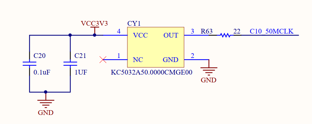
Figure 3.1 Schematics of Oscillators
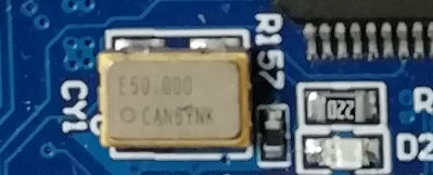
Figure 3.2 Oscillators Physical Picture
Pin Assignment
| Signal Name | FPGA Pin |
| CLK_50M | 91 |
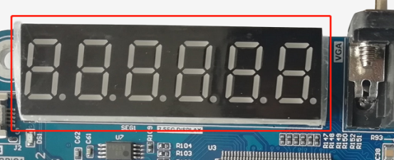
Figure 4.1 Segment Display
One type of digital tube is a semiconductor light-emitting device. The segment decoder can be divided into a seven-segment decoder and an eight-segment decoder. The difference is that the eight-segment decoder has one more unit for displaying the decimal point, the basic unit is a light-emitting diode. The segment structure of the decoder is shown below:
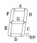
Figure 4.2 Segment Decoder Structure
Common anode decoders are used here. That is, the anodes of the LEDs are connected.
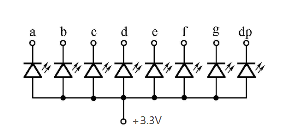
Figure 4.3 Schematics of Common Anode LED
To illuminate a segment of an 8-segment decoder, the level of the corresponding pin needs to be pulled low; when the pin is set high, the corresponding field will not light. This development board uses a 6-in-one eight-segment decoder. The schematics is shown below:
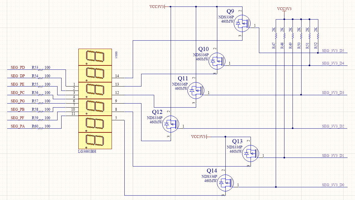
Figure 4.4 Schematic of Segment Decoders
The six-in-one decoder is a dynamic display. Due to the persistence of human vision and the afterglow effect of the LED, although the decoders are not lit at the same time, if the scanning speed is fast enough, the impression of human eyes is a group of stable display data, no flickering can be noticed. The same segments of the six-in-one decoders are connected, a total of eight pins, and with six control signal pins, a total of 14 pins, as shown in Figure 4.4. Among them SEG_PA, SEG_PB, SEG_PC, SEG_PD, SEG_PE, SEG_PF, SEG_PG, SEG_DP correspond to the A, B, C, D, E, F, G, DP of decoder; SEG_3V3_D [0..5] are six control pins of the decoders, which are also active low. When the control pin is low, the corresponding decoder is powered, so that the LED can be lit.
Pin assignments of display decoders
| Signal Name | FPGA Pin | Description |
| SEG PA | 132 | Segment A |
| SEG PB | 137 | Segment B |
| SEG PC | 133 | Segment C |
| SEG PD | 125 | Segment D |
| SEG PE | 126 | Segment E |
| SEG PF | 138 | Segment F |
| SEG PG | 135 | Segment G |
| SEG DP | 128 | Segment DP |
| SEG_3V3_D0 | 136 | Decoder 1(from right) |
| SEG_3V3_D1 | 142 | Decoder 2(from right) |
| SEG_3V3_D2 | 141 | Decoder 3(from right) |
| SEG_3V3_D3 | 129 | Decoder 4(from right) |
| SEG_3V3_D4 | 127 | Decoder 5(from right) |
| SEG_3V3_D5 | 124 | Decoder 6(from right) |
The VGA (Video Graphics Array) interface is a common interface for computer monitors. It has been used since the earliest CRT monitors and has been in use ever since. The VGA connector is a D-type connector with a total of 15 pinholes divided into 3 rows of 5 per row. More important are three RGB color component signal pins and two scan sync signals (HSYNC and VSYNC) pins.
Pins 1, 2, and 3 are the red, green, and blue primary color analog voltages, which are 0~0.714V peak-peak, 0V is colorless, and 0.714V is full color. Some non-standard displays use a full color level of 1Vpp.
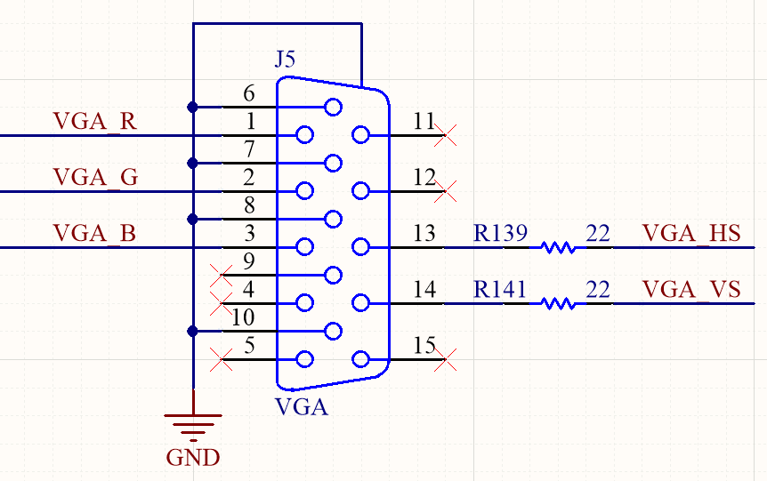
Figure 5.1 Schematics of VGA
The three primary color source and terminal matching resistors are both 75 ohms. See Figure 5.1.
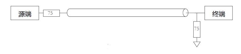
Terminal
Source
Figure 5.2 VGA Signal Transmission Diagram
HSYNC and VSYNC are line data synchronization and frame data synchronization, respectively, which are TTL levels. The FPGA can only output digital signals, and the R, G, and B required by VGA are analog signals, so we need to perform analog-to-digital conversion or DAC function. To implement a video DAC, we can use a dedicated chip or a weight resistor network. Here we use the latter as a DAC.
The development board selects the 4:4:4 mode, that is, 4 bits for red, 4 bits for green, and 4 bits for blue. The following takes red 4 bits to illustrate the selection of the resistor.
Since the DAC is a linear model, when the red 4 bits output is high, we need to get a voltage of 0.714V. The topology is shown in Figure 5.3.
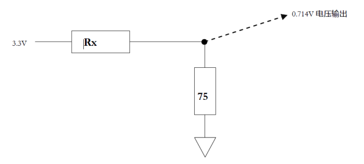
0.714V Voltage Output
Figure 5.3 Schematics of the Weight Resistance Mode Topology
The output voltage of the FPGA is 3.3V, and Rx is a parallel connection of 4 bits resistor networks, so the following equation can be obtained:
(Rx + 75)/ 3.3 = 75 / 0.714
Let the reference resistance be Ra, then:
Ra // 2Ra // 4Ra // 8Ra = Rx
According to the above two equations, the solution is obtained, Rx = 271.6, and Ra = 509.2. 500, 1k, 2k, 4k are selected for the network resistor. As shown below:
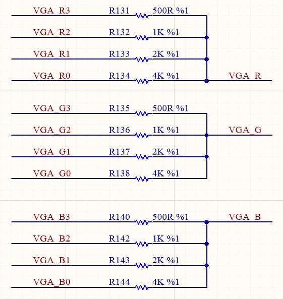
Figure 5.4 VGA Weight Resistance Network
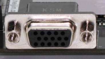
Figure 5.5 VGA Interface Physical Picture
VGA Pin Assignment
| Signal Name | FPGA Pin | Description |
| VGA HS | 98 | Horizontal Synchronous Signal |
| VGA VS | 99 | Vertical Synchronous Signal |
| VGA R0 | 100 | Red[0] |
| VGA R1 | 101 | Red[1] |
| VGA R2 | 103 | Red[2] |
| VGA R3 | 105 | Red[3] |
| VGA G0 | 106 | Green[0] |
| VGA G1 | 111 | Green[1] |
| VGA G2 | 112 | Green[2] |
| VGA G3 | 113 | Green[3] |
| VGA B0 | 114 | Blue[0] |
| VGA B1 | 115 | Blue[1] |
| VGA B2 | 119 | Blue[2] |
| VGA B3 | 120 | Blue[3] |
EEPROM is generally used in the instrumentation design. It is often used as a storage for some parameters. Data is not lost when power is off, and it is easy to operate. It is an ideal storage device.
The development board contains an EEPROM, model AT24C02, with a capacity of 2kbit (256*8bit), consisting of a 256-byte block that communicates over the IIC bus.
IIC (Inter-Integrated Circuit) literally means between integrated circuits, which is the IIC Bus abbreviation. It is a serial communication bus, using multi-master-slave architecture, by Philips in the 1980s, developed to allow motherboards, embedded systems, or mobile phones to connect to low-speed peripherals. Also written as “I2C”, “I2C”, the correct reading is “I-squared-C”.
The onboard EEPROM is designed to learn how the IIC bus communicates. See Figure 6.1 for the schematics.
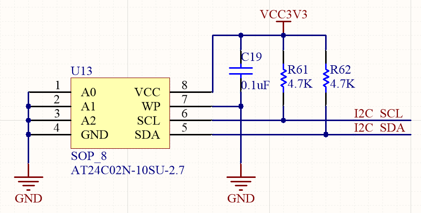
Figure 6.1 Schematics of EEPROM Physical Picture
This chip is located on the back of the development board, Figure 6.2 is the physical picture.
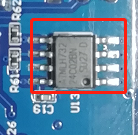
Figure 6.2 Physical Picture of EEPROM
EEPROM pin assignment
| Signal Name | FPGA Pin |
| SDA | 1 |
| SCL | 2 |
Ethernet is currently the most commonly used data communication method. Ethernet is getting faster and faster from the initial 10Mb/s to the later 100Mb/s, and to 1000Mb/s now.
The development board is equipped with an RTL8211E Gigabit Ethernet chip. The TL8211E is a highly integrated network receiving PHY chip from Realtek. It is compliant with 10Base-T, 100Base-TX and 1000Base-T IEEE802.3 standards. It can transmit network data via CAT 5 UTP cable and CAT 3 UTP cable. It belongs to the physical layer in network communication and is used for data communication between MAC and PHY. Mainly used in network interface adapters, network hubs, gateways and some embedded devices.
The main features of the RTL8211E include:
- Meets 1000Base-T IEEE802.3ab standard
- Compliant with 100Base-TX IEEE802.3u standard
- Compliant with 10Base-T IEEE802.3 standard
- Support IEEE 802.3 RGMII interface
- Support IEEE 802.3 GMII, MII interface, only RTL8211EG support
- Support for Wake-on-LAN
- Support for interrupt function
- Support crossover detection and auto-correction
- Support half-duplex, full-duplex operation
- 1000 MHz communication CAT 5 network cable can reach 100m
- RGMII interface supports 3.3V, 2.5V, 1.8V, 1.5V signals
- LED indications for three network states are available
See below for the schematics.
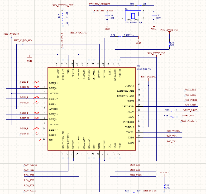
Figure 7.1 Schematics of Gigabit Ethernet Chip
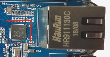
Figure 7.2 Gigabit Ethernet Physical Picture
Gigabit ethernet pin assignment
| Signal Name | FPGA Pin |
| RG0_RXCTL | 34 |
| RG0_RX0 | 33 |
| RG0_RX1 | 32 |
| RG0_RX2 | 31 |
| RG0_RX3 | 28 |
| RG0_RXCK | 24 |
| RG0_TXCK | 43 |
| RG0_TX0 | 51 |
| RG0_TX1 | 50 |
| RG0_TX2 | 49 |
| RG0_TX3 | 46 |
| RG0_TXCTL | 42 |
| NPHY_MDC | 38 |
| NPNY_MDIO | 39 |
The development board has 5 push buttons, 4 of which are programmable buttons and 1 is for system reset. The default is set high and can be pressed low. Schematics is shown in Figure 8.1.
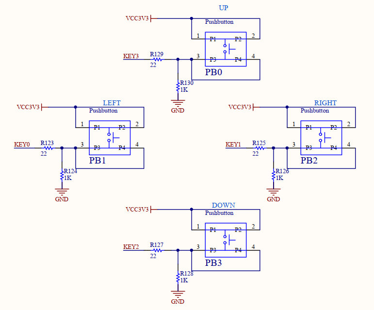
Figure 8.1 Schematics of Push Buttons
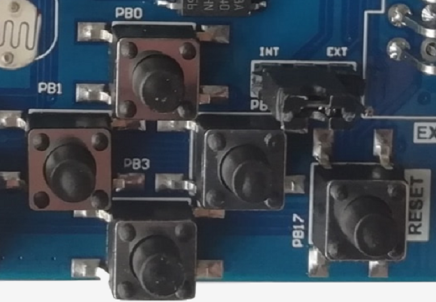
Figure 8.2 Push Button Physical Picture
Push button pin assignment
| Signal Name | FPGA Pin | Description |
| PB0 | 11 | up |
| PB1 | 3 | left |
| PB2 | 7 | right |
| PB3 | 10 | down |
9)AD/DA Thermistor, Photoresistor and Potentiometer
The PCF8591 chip is a monolithically integrated, individually powered, low power consuming, 8-bit CMOS data acquisition device. It has 4 analog inputs, 1 analog output, and 1 serial I2C bus interface. The three address pins A0, A1 and A2 of PCF8591 can be used for hardware address programming (the three addresses on the development board are connected to GND, that is, the device address is 7’B1001000), allowing access on the same I2C bus. PCF8591 devices without additional hardware. The address, control, and data signals input and output on the PCF8591 device are serially transmitted over a two-wire bidirectional I2C bus. Chip features of PCF8591:
- Operating voltage range 2.5V-6V
- Low standby current
- Serial input/output via I2C bus
- I2C address selection by 3 hardware address pins
- Max sampling rate given by I2C bus speed
- 4 analog inputs configurable as single ended or differential inputs
- Auto-incremented channel selection
- Analog voltage ranges from VSS to VDD
- On-chip track and hold circuit
- 8-bit successive approximation A/D conversion
- Multiplying DAC with one analog output
The schematics is shown in Figure 9.1:

Figure 9.1 Schematics of AD/DA
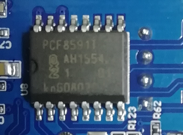
Figure 9.2 PCF8591 Physical Picture
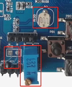
Figure 9.3 Potentiometer, Photoresistor, and Thermistor
PCF8591 pin assignment
| Signal Name | FPGA Pin |
| ADDA_I2C_SAD | 52 |
| ADDA_I2C_SCL | 53 |
The 8-bit DIP switch is onboard, which share the pins of the FPGA with the 8-bit LEDs. The FPGA pin gets high when the DIP switch is turned on. The schematics is shown as follows:
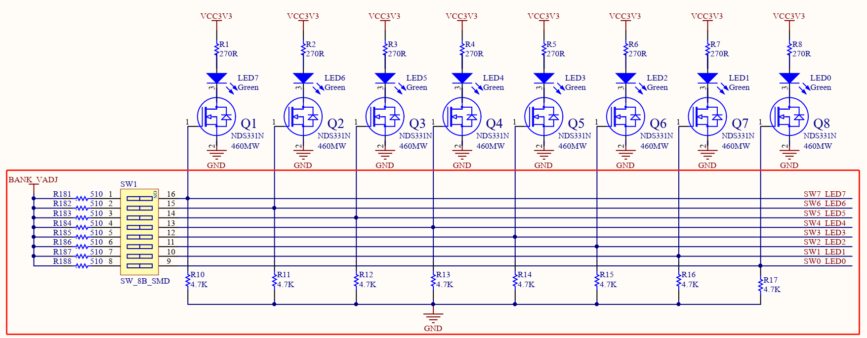
Figure 10.1 Schematics of DIP Switches
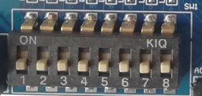
Figure 10.2 DIP Switches Physical Picture
Note that the number marked on the device, 1-8, is not the number in the circuit design. In the schematics, SW0 corresponds to the first switch from right to left in the physical picture, and SW1 corresponds to the second switch in physical picture from right to left, and so on.
DIP switches pin assignment
| Signal Name | FPGA Pin | Description |
| SW0_LED0 | 80 | First from right to left |
| SW1_LED1 | 83 | Second from right to left |
| SW2_LED2 | 86 | Third from right to left |
| SW3_LED3 | 87 | Fourth from right to left |
| SW4_LED4 | 74 | Fifth from right to left |
| SW5_LED5 | 75 | Sixth from right to left |
| SW6_LED6 | 76 | Seventh from right to left |
| SW7_LED7 | 77 | Eighth from right to left |
The development board has eight LEDs. When the pin is high, the LED emits light. When it is low, the LED does not illuminate. It should be noted that, as mentioned in the previous section, the LED and the DIP switch share the FPGA pin. When the FPGA pin is not output, due to the characteristics of the circuit itself, the corresponding LED will also be lit when the DIP switch is closed. If the PFGA pin has an output, the output is high, the LED will remain lit. If the FPGA output is low, the LED will extinguish. In other words, the LED light is only controlled by the FPGA and is not controlled by the switch. The schematic is shown in Figure 11.1.
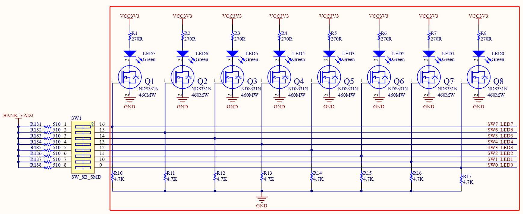
Figure 11.1 Schematics of LED
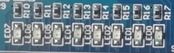
Figure 11.2 8-bit LED Physical Picture
LED pin assignment
| Signal Name | FPGA pin | Description |
| SW0_LED0 | 80 | First from right to left |
| SW1_LED1 | 83 | Second from right to left |
| SW2_LED2 | 86 | Third from right to left |
| SW3_LED3 | 87 | Fourth from right to left |
| SW4_LED4 | 74 | Fifth from right to left |
| SW5_LED5 | 75 | Sixth from right to left |
| SW6_LED6 | 76 | Seventh from right to left |
| SW7_LED7 | 77 | Eighth from right to left |
The N25Q128A is a serial FLASH chip with a capacity of 128Mbit, which is more than enough for storing programs in the FPGA. Figure 12.1 shows the N25Q128A in the schematics.
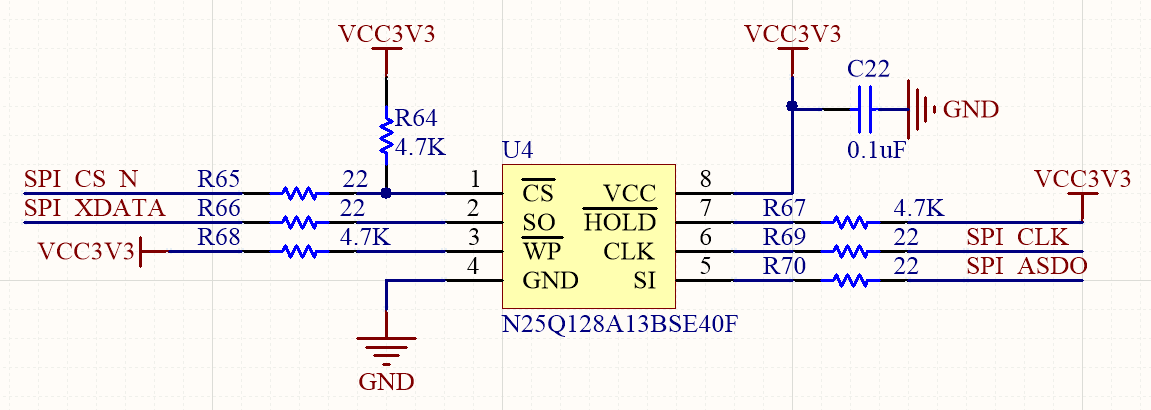
Figure 12.1 Schematics of FLASH
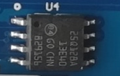
Figure 12.2 FLASH Physical Picture
The development board reserves two GPIO interfaces, P1 and P2. The P1 interface contains 6 standard IO pin PFGA resources, 2 GND signals, and 2 adjustable power signals. The P2 interface contains 3 pairs of LVDS signals, which can also be used as 6 standard IOs; 1 pair of clock signals can be used as ordinary clocks or LVDS clocks, or 2 standard IO or 1 pair LVDS signals; 2 GND Signal, and 2 adjustable power signals. The schematics is as follows:
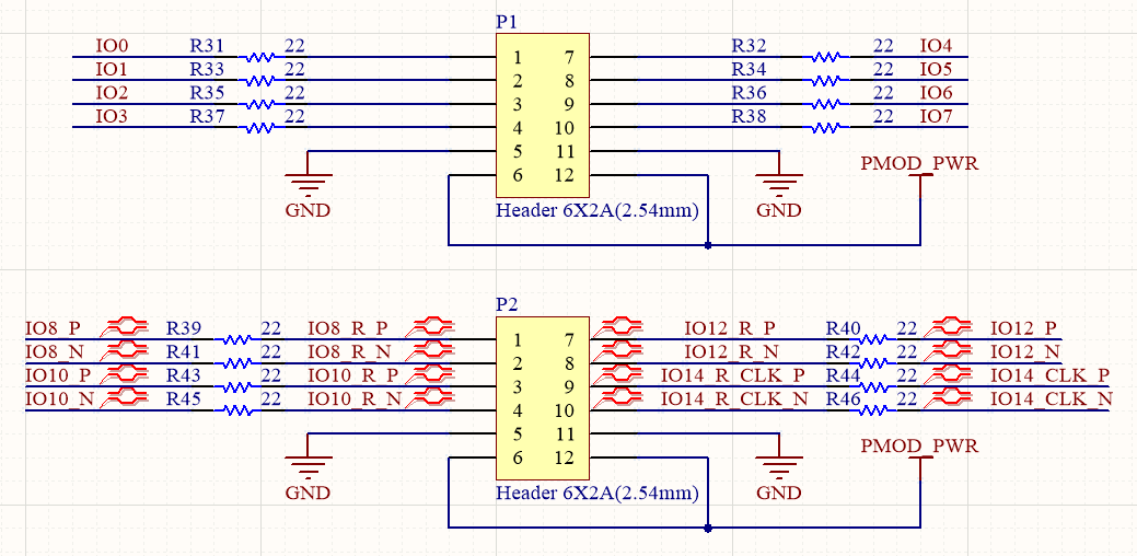
Figure 13.1 Schematics of GPIO
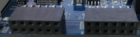
Figure 13.2 GPIO Physical Picture
GPIO pin assignment
| Signal Name | FPGA Pin | Description |
| IO0 | 72 | P1-1/standard IO |
| IO1 | 68 | P1-2/ standard IO |
| IO2 | 66 | P1-3/ standard IO |
| IO3 | 58 | P1-4/ standard IO |
| GND | P1-5/GND | |
| VCC | P1-6/VCC | |
| IO4 | 73 | P1-7/ standard IO |
| IO5 | 69 | P1-8/ standard IO |
| IO6 | 67 | P1-9/ standard IO |
| IO7 | 65 | P1-10/ standard IO |
| GND | P1-11/GND | |
| VCC | P1-12/VCC | |
| IO8_P | 54 | P2-1/LVDS_P |
| IO8_N | 55 | P2-2/LVDS_N |
| IO10_P | 70 | P2-3/LVDS_P |
| IO10_N | 71 | P2-4/LVDS_N |
| GND | P2-5/GND | |
| VCC | P2-6/VCC | |
| IO12_P | 59 | P2-7/LVDS_P |
| IO12_N | 60 | P2-8/LVDS_N |
| IO14_CLK_P | 84/88 | P2-9/LVDS_CLK_P |
| IO14_CLK_N | 85/89 | P2-10/LVDS_CLK_N |
| GND | P2-11/GND | |
| VCC | P2-12/VCC |
PRA006/010 can be used as a full-featured development board or as a JTAG adapter. When used as a development board, as described in the introduction to this document, you need to connect the J9 jumper to the “INT” position so that the USB can download the program for the board FPGA; if you connect the J9 jumper to “EXT” “Location, the development board can be used as a downloader.
In addition, the JTAG connection port contains a set of serial communication lines, which can be used as a serial communication for the development board. The JTAG principle is shown in Figure 14.1:

Figure 14.1 Schematics of JTAG Interface
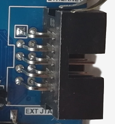
Figure 14.2 JTAG Physical Picture
JTAG pin assignment
| Signal Name | FPGA Pin | Description |
| TCK | 16(TCK) | JTAG pin 1 |
| GND | JTAG pin 2 | |
| TDO | 20(TDO) | JTAG pin 3 |
| VCC | JTAG pin 4 | |
| TMS | 18(TMS) | JTAG pin 5 |
| TXD | 144 | JTAG pin 6 |
| SRST | JTAG pin 7 | |
| RXD | 143 | JTAG pin 8 |
| TDI | 15(TDI) | JTAG pin 9 |
| GND | JTAG pin 10 |
References
- http://www.mouser.com/ds/2/149/NDS331N-116501.pdf
- https://www.mouser.com/ds/2/268/atmel_doc0180-1065439.pdf
- https://www.nxp.com/docs/en/data-sheet/PCF8591.pdf
- https://www.macronix.com/Lists/ApplicationNote/Attachments/1947/AN0244V1%20-%20Comparing%20Micron%20N25Q128A%20with%20Macronix%20MX25U12835F.pdf