High-speed ADC9226 Acquisition Experiment (FII-BD9226) – parallel ADC collectors and master the use of ADC9226 – FII-PRA040 Altera Risc-V Experiment 18
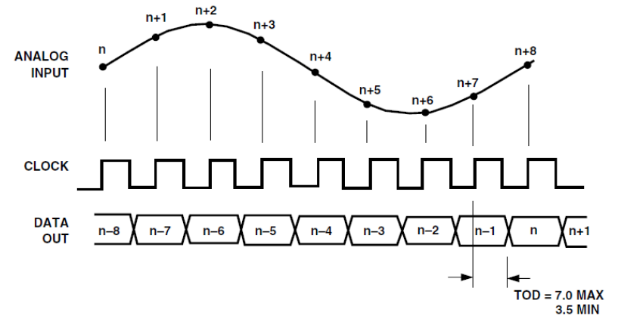
Experiment 18 High-speed ADC9226 Acquisition Experiment 18.1 Experiment Objective Learn about parallel ADC collectors and master the use of ADC9226. 18.2 Experiment Implement Insert the ADC9226 module face up into the FPGA development board to the GPIO2 and GPIO1 ports which are next to the red-green audio module. Write programs to use this module to test 18.3 Experiment 18.3.1 ADC9226 Module Introduction ADC9226 module adopts AD9226 chip design of ADI Company. This chip is a monolithic, 12-bit, 65 MSPS analog-to-digital converter (ADC). It uses a single power supply and…
Read More
