Virtual Box
FII-BD7100 FII-PE7030 PetaLinux SOC Tutor

Step by Step Installation of PetaLinux on Ubuntu via VirtualBox in FPGA Development Board

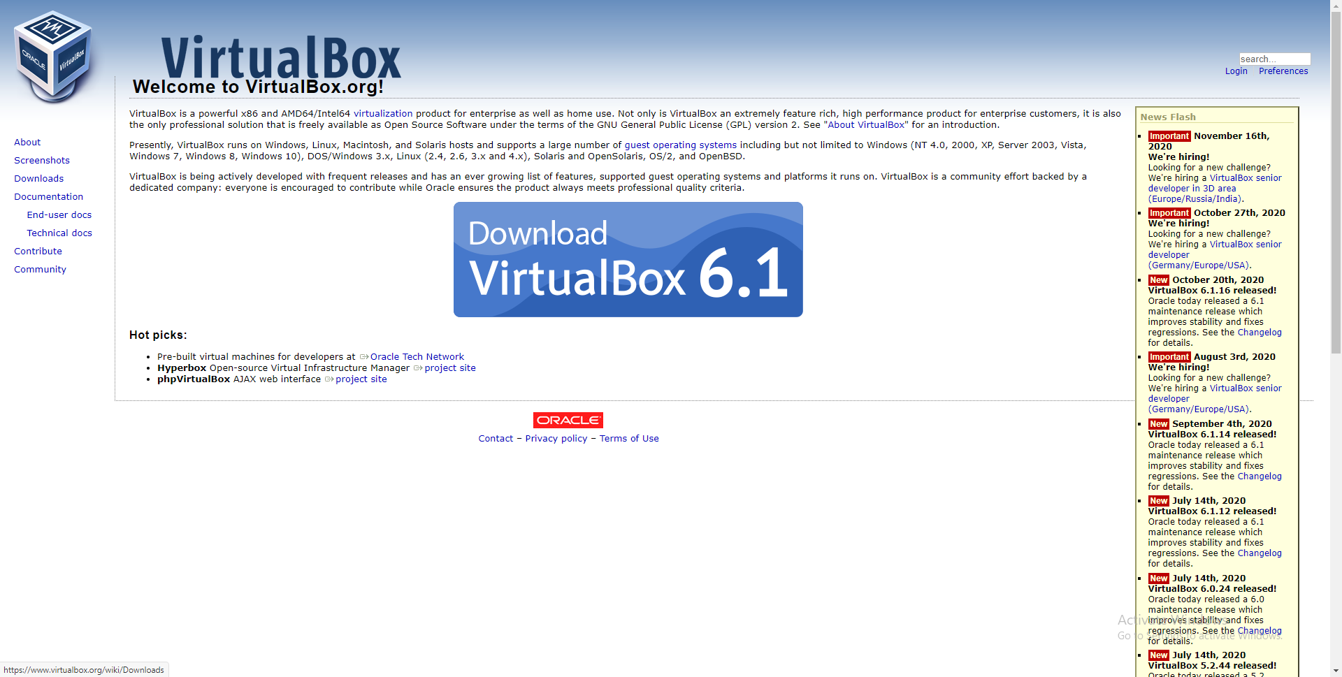
Table of Contents Copyright Notice 2 Section 0: Prerequisites 3 Section 1: Creating your first Virtual Machine using VirtualBox 3 1.1 Installing VirtualBox 3 1.2 Creating a Virtual Machine Part 1 – Setting up the VirtualBox environment 7 1.3 Creating a Virtual Machine Part 2 – Downloading and installing Ubuntu 12 Section 2: Setting up Ubuntu for PetaLinux 22 2.1 Creating a Snapshot 22 2.2 Getting familiar with Ubuntu – Shutting down & Restart 25 2.3 Getting familiar with Ubuntu – Changing the properties 26 Section 3: Installing and Working…

Read More
Text Description automatically generated
FII-BD7100 FII-PE7030 SOC Tutor

Basic Introduction to Device Tree Driver Development

Basic Introduction to Device Tree Driver Development Copyright Notice: © 2020 Fraser Innovation Inc ALL RIGHTS RESERVED Without written permission of Fraser Innovation Inc, no unit or individual may extract or modify part of or all the contents of this manual. Offenders will be held liable for their legal responsibility. Thank you for purchasing the FPGA development board. Please read the manual carefully before using the product and make sure that you know how to use the product correctly. Improper operation may damage the development board. This manual is constantly…

Read More
FPGA Development Board Altera Xilinix Risc-V SoC FII-PE7030
FII-PE7030

FII-PE7030 FPGA Development Board and Educational Platform Experimental Manual and Haredware Reference Guide

FII-PE7030 Hardware Reference Guide EVB Board – FII-PE7030 User Experimental Manuals Introduction to Zynq_7030 Development System FII-PE7030 zynq_7030 Main Resources Usage and FPGA Development Experiemnt zynq xc7z030 board – FII-PE7030 Experiment 1 LED Shifting Design zynq xc7z030 board – FII-PE7030 Experiment 2 – Analysis of Switch Signals via ILA zynq xc7z030 board – FII-PE7030 Experiment 3 – Segment Display Digital Clock Experiment zynq xc7z030 board – FII-PE7030 Experiment 4 – Button Debounce zynq xc7z030 board – FII-PE7030 Experiment 5 – Digital Clock Comprehensive Experiment zynq xc7z030 board – FII-PE7030 Experiment…

Read More
ADC9226 timing diagram
Experimental Manuals FII-PRA040 FPGA Board Based FPGA Tutor Risc-V

High-speed ADC9226 Acquisition Experiment (FII-BD9226) – parallel ADC collectors and master the use of ADC9226 – FII-PRA040 Altera Risc-V Experiment 18

  Experiment 18 High-speed ADC9226 Acquisition Experiment 18.1 Experiment Objective Learn about parallel ADC collectors and master the use of ADC9226. 18.2 Experiment Implement Insert the ADC9226 module face up into the FPGA development board to the GPIO2 and GPIO1 ports which are next to the red-green audio module. Write programs to use this module to test 18.3 Experiment 18.3.1 ADC9226 Module Introduction ADC9226 module adopts AD9226 chip design of ADI Company. This chip is a monolithic, 12-bit, 65 MSPS analog-to-digital converter (ADC). It uses a single power supply and…

Read More