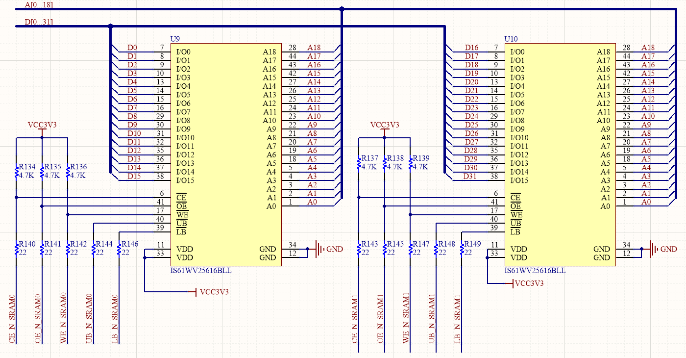
DDS block diagram
Experimental Manuals FII-PRA040 Risc-V

DAC9767 DDS Signal Source Experiment, AD9767 datasheet and use the AD9767 to design a signal source that can generate sine, square, triangle, and sawtooth waves – FII-PRA040 Altera Risc-V Experiment 19

Experiment 19 DAC9767 DDS Signal Source Experiment 19.1 Experiment Objective Learn about DDS (Direct Digital Synthesizer) related theoretical knowledge. Read the AD9767 datasheet and use the AD9767 to design a signal source that can generate sine, square, triangle, and sawtooth waves. 19.2 Experiment Implement Learn about DDS theoretical knowledge. On the basis of understanding the principle of DDS, combined with the theoretical knowledge, use AD9767 module and development board to build a signal source whose waveform, amplitude and frequency can be adjusted. (There are no specific requirements for the adjustment…

Read More
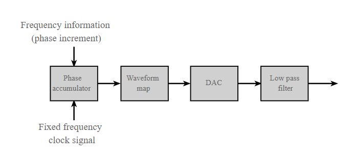
chematics of SRAM
FII-PRA040 FPGA Board Based FPGA Tutor Risc-V

How does SRAM read and write work ? Review frequency division, button debounce, and hex conversion experiment – FII-PRA040 Altera Risc-V Tutorial Experiment 15

Experiment 15 SRAM Read and Write 15.1 Experiment Objective Learn the read and write of SRAM Review frequency division, button debounce, and hex conversion experiment content 15.2 Experiment Implement Control the read and write function of SRAM by controlling the button The data written to the SRAM is read out again and displayed on the segment display In the process of reading data, it is required to have a certain time interval for each read operation. 15.3 Experiment 15.3.1 Introduction to SRAM SRAM (Static Random-Access Memory) is a type of…

Read More