How does SRAM read and write work ? Review frequency division, button debounce, and hex conversion experiment – FII-PRA040 Altera Risc-V Tutorial Experiment 15
Experiment 15 SRAM Read and Write
15.1 Experiment Objective
- Learn the read and write of SRAM
- Review frequency division, button debounce, and hex conversion experiment content
15.2 Experiment Implement
- Control the read and write function of SRAM by controlling the button
- The data written to the SRAM is read out again and displayed on the segment display
- In the process of reading data, it is required to have a certain time interval for each read operation.
15.3 Experiment
15.3.1 Introduction to SRAM
SRAM (Static Random-Access Memory) is a type of random access memory. The “static” means that as long as the power is on, the data in the SRAM will remain unchanged. However, the data will still be lost after power turned off, which is the characteristics of the RAM.
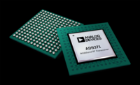
Two SRAMs (IS61WV25616BLL) are on the development board, each SRAM has 256 * 16 words of storage space. Each word is 16-bit. The maximum read and write speed can reach 100 MHz. The physical picture is shown in Figure 15.1.
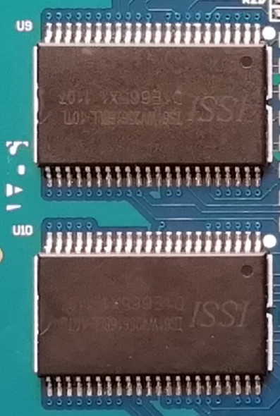
Figure 15.1 SRAM physical picture
15.3.2 Hardware Design
As shown in Figure 15.2, a set of control signals (low signal is valid): chip selection signal CE, read control signal OE, write enable control number WE, and two byte control signals UB and LB, through CE_N_SRAM, OE_N_SRAM, WE_N_SRAM, UB_N_SRAM, LB_N_SRAM, connect to the FPGA, and the read and write status is controlled by the FPGA. The address is sent to the SRAM through the address line A[17:0]. In the write state, the data to be written is sent to the SRAM through the data line D[15:0], and can be written into the register of the corresponding address; In the read state, the data in the corresponding address register can be directly read into the FPGA by the data line.
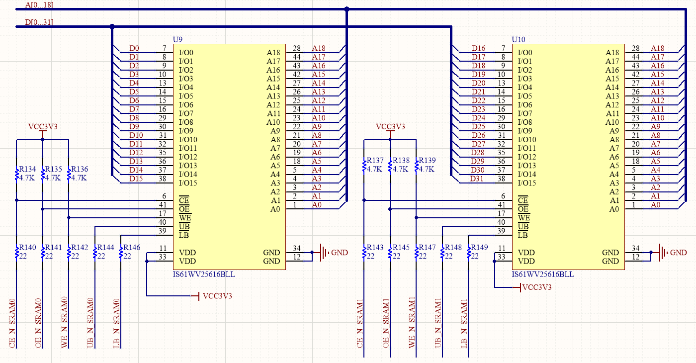
Figure 15.2 Schematics of SRAM
15.3.3 Introduction to the Program
This experiment will use the frequency division, button debounce, hex conversion and segment display module. (Refer to the previous experiment for more information) Here SRAM read and write module is mainly introduced.
The first step: the establishment of the main program framework
|
The inputs are 50 MHz system clock IN_CLK_50M, button module PB[7:1], PB[3] (RETURN) as external hardware reset, PB[2] (UP) as write control, PB[7] (DOWN) as read control. The output has two sets of control signals to control two srams respectively, specifically chip selection signal sram_cs_n, write control signal sram_we_n, read control signal sram_oe_n, and byte control signals sram_ub_n and sram_lb_n, address bus sram_daddr[17:0], data bus Sram_data[31:0], and the segment display bit selection signal tube_sel[5:0] and the segment selection signal tube_seg[7:0].
The second step: SRAM read and write module
In this experiment, two SRAMs are used simultaneously and are expanded into a 32-bit wide data memory.
|
In the write state, the write enable wr_en is pulled high. At this time, sram_data is the data wr_data to be written. In other cases, the write enable is pulled low. In the read state, the data is directly read into the FPGA by sram_data.
At reset, the SRAM control signals are all pulled high, then jumps to the 0 state, and the data is read and written by the state machine.
0 state: an initial address “511” is given, and an initial data “123456”, when the write enable signal PB_flag[2] is valid, the chip selection signal pulls down the selected SRAM. The write control signal is pulled low to prepare for write operation, and the read control signal remains pulled up. Meanwhile, the byte control signal is pulled low, indicating that the high and low two bytes of data are simultaneously written and then jump to the 1 state. When the read enable signal PB_flag[7] is active, in contrast to the write enable, the write control signal is held high, the read control signal is pulled low to prepare for the read operation, and jumps to the 2 state.
1 state: starting from the initial address “511”, writing initial data “123456”, each clock cycle address and data are simultaneously decremented by one, performing 512 data continuous write operations. When the register address bit is ‘0’, end the write operation and jum to the 4 state.
2 state: Starting from the initial address “511”, the address is decremented by 1 every 1 second under the control of the second pulse s_flag, and a continuous read operation of 512 data is performed. When the data is completely read, the address jumps to the 4 state when the address is ‘0’.
4 state: The control signals are all pulled high, deactivate the control of the SRAM, jumping to the ‘0’ state, an waiting for the next operation.
15.4 Experiment Verification
The first step: pin assignment
Table 15.1 SRAM read and write experiment pin mapping
The second step: board verification
After the pin assignment is completed, the compilation is performed, and the board is verified after passing.
After the development board is programmed, the segment display will all light up, but because no data is read, the segment display will display all ‘0’s, as shown in Figure 15.3. Press the PB[2] (UP) button to write the data to the SRAM, and then press the PB[7] (DOWN) button to read the written data.
At this time, it displays “123456” and decrement by one every second.
See Figure 15.4. From this it is verified that the specified data is written into the SRAM and is read correctly.
Figure 15.3 SRAM write and read 1
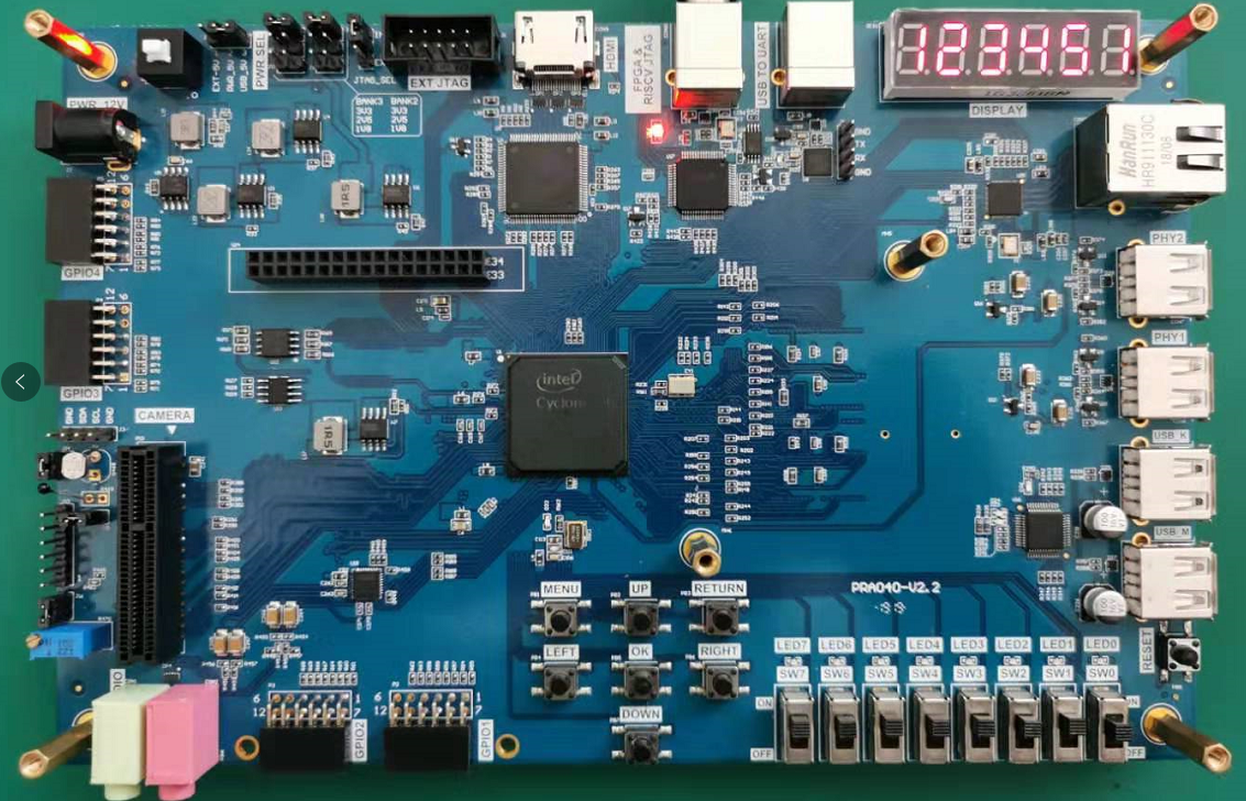
Figure 15.4 SRAM write and read 2