BCD decoder, Display design of hexadecimal to 7 segment display decoders, Achieve digital clock display – zynq xc7z030 board – FII-PE7030 Experiment 3 – Segment Display Digital Clock Experiment
3.1 Experiment Objective
- Review the contents of experiment 1 and experiment 2, master the configuration of PLL, the design of frequency divider, the principle of schematics and the pin assignment of FPGA. Familiar with the design of Verilog’s tree hierarchy
- Study BCD decoder
- Display design of hexadecimal to 7 segment display decoders
- Achieve digital clock display
3.2 Experiment Implement
- The display decoder has two lower digits to display seconds, the middle two digits to display minutes, and the highest two digits to display hours.
- Separate the seconds, minutes, and hours with decimal points
3.3 Experiment
3.3.1 Introduction to Segment Display Decoder
One type of segment display is a semiconductor light-emitting device. The segment display can be divided into a seven-segment display decoder and an eight-segment display decoder. The difference is that the eight-segment display decoder has one more unit for displaying the decimal point, the basic unit is a light-emitting diode. The on-board segment display is a six-in-one eight-segment display decoder as shown in Figure 3.1, and its structure is shown in Figure 3.2.
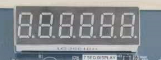
Figure 3.1 Segment display decoder physcial picture
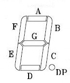
Figure 3.2 Segment decoder structure
Common anode decoders are used here. That is, the anodes of the LEDs are connected. See Figure 3.3. Therefore, the FPGA is required to control the cathode of the LED to be low level, illuminate the diode, and display the corresponding information. The six-digit common anode eight-segment display decoder refers to the signal that controls which one is lit, which is called the bit selection signal. The content displayed by each digital segment is called the segment selection signal. The corresponding truth table is shown in Table 3.1.
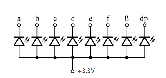
Figure 3.3 Schematics of common anode decoders
Table 3.1 8-segment display decoder truth table
| Signal Segment | DP | G | F | E | D | C | B | A |
| · | 0 | 1 | 1 | 1 | 1 | 1 | 1 | 1 |
| 0 | 1 | 1 | 0 | 0 | 0 | 0 | 0 | 0 |
| 1 | 1 | 1 | 1 | 1 | 1 | 0 | 0 | 1 |
| 2 | 1 | 0 | 1 | 0 | 0 | 1 | 0 | 0 |
| 3 | 1 | 0 | 1 | 1 | 0 | 0 | 0 | 0 |
| 4 | 1 | 0 | 0 | 1 | 1 | 0 | 0 | 1 |
| 5 | 1 | 0 | 0 | 1 | 0 | 0 | 1 | 0 |
| 6 | 1 | 0 | 0 | 0 | 0 | 0 | 1 | 0 |
| 7 | 1 | 1 | 1 | 1 | 1 | 0 | 0 | 0 |
| 8 | 1 | 0 | 0 | 0 | 0 | 0 | 0 | 0 |
| 9 | 1 | 0 | 0 | 1 | 0 | 0 | 0 | 0 |
| A | 1 | 0 | 0 | 0 | 1 | 0 | 0 | 0 |
| B | 1 | 0 | 0 | 0 | 0 | 0 | 1 | 1 |
| C | 1 | 1 | 0 | 0 | 0 | 1 | 1 | 0 |
| D | 1 | 0 | 1 | 0 | 0 | 0 | 0 | 1 |
| E | 1 | 0 | 0 | 0 | 0 | 1 | 1 | 0 |
| F | 1 | 0 | 0 | 0 | 1 | 1 | 1 | 0 |
There are two ways to display the decoders, static display and dynamic display.
Static display: each display segment is connected with an 8-bit data line to control and maintain the displayed glyph until the next segment selection signal arrives. The advantage is that the driver is simple, and the disadvantage is that it takes up too much I/O resources.
Dynamic display: parallel the segment selection lines of all display decoders, and the digit selection line controls which digit is valid and lights up. Through the afterglow effect of the LED and the persistence effect of the human eye, the display decoder appears to be continuously lit at a certain frequency. The advantage is to save I / O resources, the disadvantage is that the driver is more complicated, the brightness is not high as static display.
In this experiment, the segment display was driven by dynamic scanning.
3.3.2 Hardware Design
The schematics of the segment display is shown in Figure 3.4. The anode is connected to VCC through the P-channel field corresponding tube. Therefore, when the bit selection signal SEG_3V3_D[0:5] is low level 0, the FET is turned on, the anode of the display decoder is high level; the cathode (segment selection signal) SEG_PA, SEG_PB, SEG_PC, SEG_PD, SEG_PE, SEG_PF, SEG_PG, SEG_DPZ are directly connected to the FPGA and directly controlled by the FPGA. Therefore, when the bit selection signal is 0, and the segment selection signal is also 0, the segment display is lit.
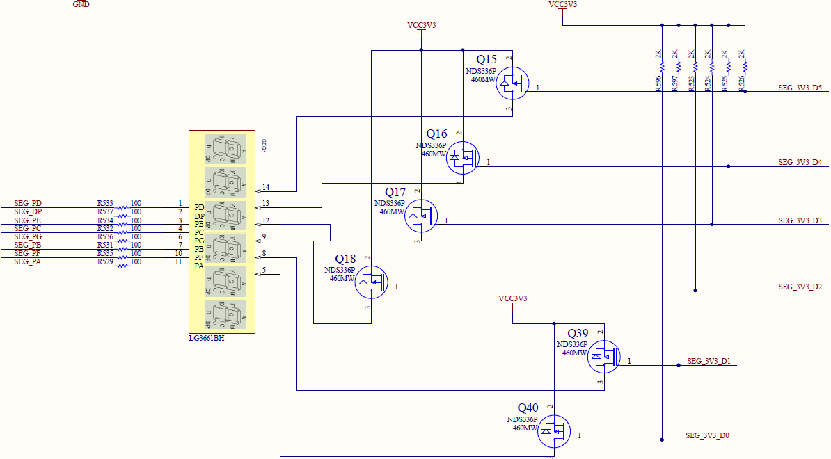
Figure 3.4 Schematics of the segment display
3.3.3 Program Design
The first step: the establishment of the main program framework (interface design)
| module BCD_counter(
input inclk_p, input inclk_n, input rst, output reg [7:0] tube_seg, output reg [5:0] tube_sel ); endmodule |
The input signal has a clock and a reset signal, and the output signal is a segment selection signal seven_seg and a new signal scan.
Refer to Experiment 1 for the control module, frequency division module and counting module.
The second step: system control module
| module sys_control(
input inclk_p, input inclk_n, input rst, output sys_clk, output reg sys_rst, output reg ext_rst ); wire pll_locked; //PLL instantiation clk_wiz_0 clk_wiz_0_inst( .clk_in1_p (inclk_p), .clk_in1_n (inclk_n), .reset (1’b0), .locked (pll_locked), .clk_out1 (sys_clk) ); //reset signal always @ (posedge sys_clk) begin sys_rst <= !pll_locked; ext_rst <= rst; end endmodule |
In the first sub-module (system control module), the input clock is the system 200 MHz differential clock, and a 100MHz is output through the PLL as the working clock of the other sub-modules. At the same time, the PLL lock signal pll_locked is inverted as the system reset signal, and the key reset rst is registered as the external hardware reset signal est_rst.
The third step: frequency division
With reference to Experiment 1, a millisecond pulse signal and a second pulse signal are output as input signals of the segment display driving module.
The fourth step: segment display driving module
- Counting section
The counting part is similar to the frequency dividing module. It is timed by the second pulse signal for 60 seconds, 60 minutes, 24 hours, and when the time reaches 23 hours, 59 minutes and 59 seconds, the counters are all cleared, which is equivalent to one day.
- Segment display dynamic scanning part
| // Segment display dynamic scanning, implemented by the state machine
reg count_seg; reg point; reg scan_state reg [3:0] counta,countb; //second counter reg [3:0] countc,countd; //minute counter reg [3:0] counte,countf; //hour counter always @ (posedge clk) begin if(rst) begin tube_sel <= 6’b111_111; count_seg <= 4’d0; point <= 1’b1; scan_state <= 0; end else case (scan_state) 0 : begin tube_sel <= 6’b111_110; count_seg <= counta; point <= 1’b1; if (ms_f) scan_state <= 1; end
1 : begin tube_sel <= 6’b111_101; count_seg <= countb; point <= 1’b1; if (ms_f) scan_state <= 2; end
2 : begin tube_sel <= 6’b111_011; count_seg <= countc; point <= 1’b0; if (ms_f) scan_state <= 3; end
3 : begin tube_sel <= 6’b110_111; count_seg <= countd; point <= 1’b1; if (ms_f) scan_state <= 4; end
4 : begin tube_sel <= 6’b101_111; count_seg <= counte; point <= 1’b0; if (ms_f) scan_state <= 5; end
5 : begin tube_sel <= 6’b011_111; count_seg <= countf; point <= 1’b1; if (ms_f) scan_state <= 0; end
default : scan_state <= 0; endcase end |
The dynamic scanning of the segment display is realized by the state machine. A total of six segment display require six states. The state machine scan_state[2:0] is defined, and the corresponding content count_sel is displayed in different states. At reset, all six segment display are extinguished and jump to the 0 state. The segment display is dynamically scanned in 1 millisecond time driven by a millisecond pulse:
In the 0 state, the 0th segment display is lit, and the ones digit of the second is displayed;
In the 1 state, the first segmentdisplay is lit, and the tens digit of the second is displayed;
In the 2 state, the second segment display is lit, and the ones digit of the minute is displayed, the decimal point lights up, distinguishing between seconds and minutes;
In the 3 state, the third segment display is lit, and the tens digit of the minute is displayed;
In the 4 state, the fourth segment display is lit, and the ones digit of the hour is displayed, the decimal point lights up, distinguishing between minutes and hours;
In the 5 state, the fifth segment display is lit, and the tens digit of the hour is displayed;
The third step: segment code display section
| always @ (posedge sys_clk)
begin if (ext_rst) tube_seg <= 8’d0; else case (counta) 0 : tube_seg <= 8’b0100_0000; 1 : tube_seg <= 8’b0111_1001; 2 : tube_seg <= 8’b0010_0100; 3 : tube_seg <= 8’b0011_0000; 4 : tube_seg <= 8’b0001_1001; 5 : tube_seg <= 8’b0001_0010; 6 : tube_seg <= 8’b0000_0010; 7 : tube_seg <= 8’b0111_1000; 8 : tube_seg <= 8’b0000_0000; 9 : tube_seg <= 8’b0001_0000; default : tube_seg <= 8’b0100_0000; endcase end // Set decimal points between seconds, minites, and hours always @ (posedge clk) tube_seg <= {point, seven_seg_r}; |
Referring to Table 3.1, the characters to be displayed are corresponding to the segment code, and the decimal point is composed of the final segment selection signal tube_seg in the form of bit splicing.
3.4 Experiment Verification
The first step: add contraints and assign pins
The pin assignments are shown in Table 3.2.
Table 3.2 Segment display experimental pin mapping table
| Signal Name | Network Name | FPGA Pin | Port Description |
| inclk_p | SYSCLK_P | AC13 | Input Clocl (differential)
200MHz |
| inclk_n | SYSCLK_N | AD13 | |
| rst | GPIO_SW_2 | F4 | reset |
| scan[0] | SEG_D0 | C1 | Bit Selection Signal |
| scan[1] | SEG_D1 | E3 | |
| scan[2] | SEG_D2 | F7 | |
| scan[3] | SEG_D3 | D6 | |
| scan[4] | SEG_D4 | H11 | |
| scan[5] | SEG_D5 | J11 | |
| seven_seg[0] | SEF_PA | J10 | Segment Selection Signal |
| seven_seg[1] | SEF_PB | J9 | |
| seven_seg[2] | SEF_PC | A7 | |
| seven_seg[3] | SEF_PD | B7 | |
| seven_seg[4] | SEF_PE | A8 | |
| seven_seg[5] | SEF_PF | A9 | |
| seven_seg[6] | SEF_PG | A10 | |
| seven_seg[7] | SEF_DP | B10 |
The second step: run the implementation, generate bitstream files, and verify the board
After successfully downloading the generated programmable bitstream file to the Zynq_7030 development board, the experimental phenomenon is shown in Figure 3.5.

Figure 2.3 Segment display experimental phenomenon