SOPC (NiosII) system, simulation and verification of RISC-V CPU, Basic FPGA design training, IC design and verification – Altera Risc-V Board Tutorial : Introduction of FII-PRA040 Development System
1、Design Objective of the System
The main purpose of this system design is to complete FPGA learning, development and experiment with Intel Quartus. The main device uses the Inte Cyclone10 10CL040YF484C8G and is currently the latest generation of FPGA devices from Intel. The major learning and development projects can be completed as follows:
- Basic FPGA design training
- Construction and training of the SOPC (NiosII) system
- IC design and verification, the system provides hardware design, simulation and verification of RISC-V CPU
- Development and application based on RISC-V
- The system is specifically optimized for hardware design for RISC-V system applications
2、System Resource
- Extended memory: Two Super Sram (IS61WV51216, 512K x 32bit) are connected in parallel to form a 32-bit data interface, and the maximum access space is up to 2M bytes.
- Serial flash: Spi interface serial flash (16M bytes)
- Serial EEPROM
- Gigabit Ethernet: 100/1000 Mbps
- USB to serial interface: USB-UART bridge
3、Human-computer Interaction Interface
- 8 DIP switches
- 8 push buttons, definition of 7 push buttons: MENU, UP, RETUN, LEFT, OK, RIGHT, DOWN, 1 for reset: RESET
- 8 LEDs
- 6 7-segment LED display
- I2C bus interface
- UART external interface
- Two JTAG programming interfaces: One is for downloading the FPGA debug interface, and the other is the JTAG debug interface for RISC-V CPU
- Built-in RISC-V CPU software debugger, no external RISC-V JTAG emulator required
- 4 12-pin GPIO connectors, in line with PMOD interface standards
4、Software Development System
- Quartus 18.0 and later version for FPGA development, Nios-II SOPC
- Freedom Studio-Win_x86_64 software development for RISC-V CPU
5、Supporting Resources
RISC-V JTAG Debugger
Intel Altera JTAG Download Debugger
FII-PRA040 User Experimental Manual
FII-PRA040 Hardware Reference Guide
6、Physical Picture
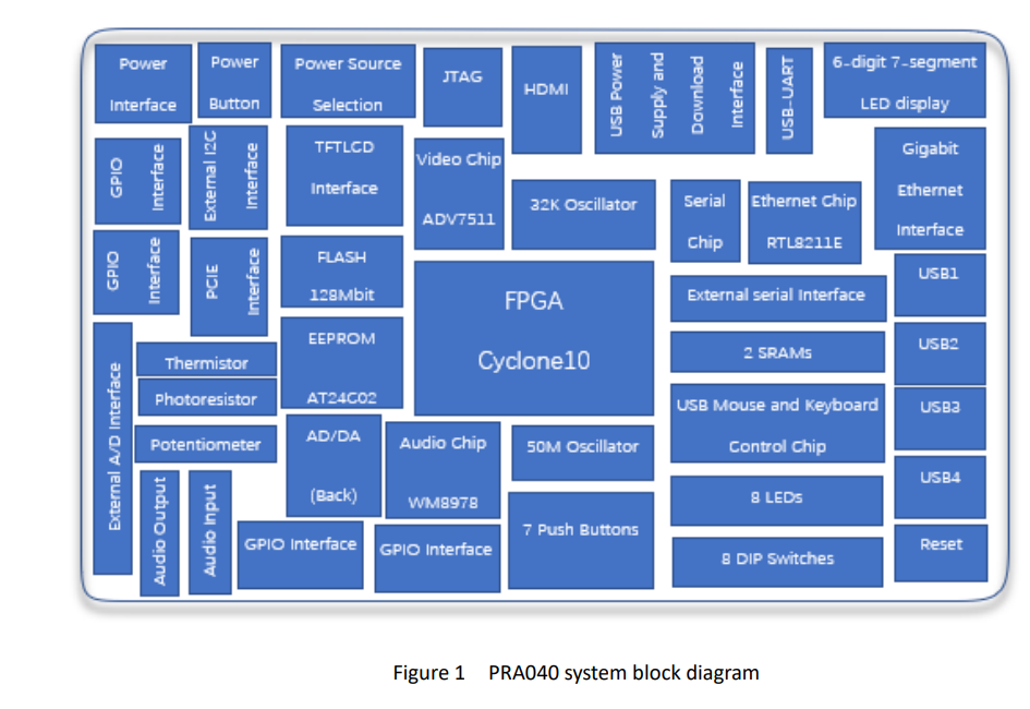
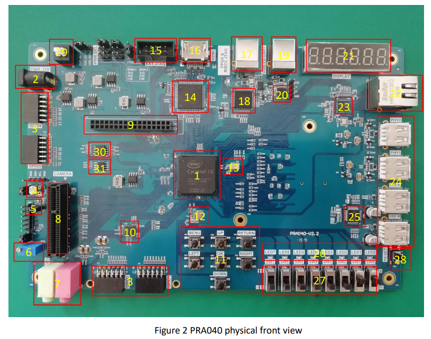
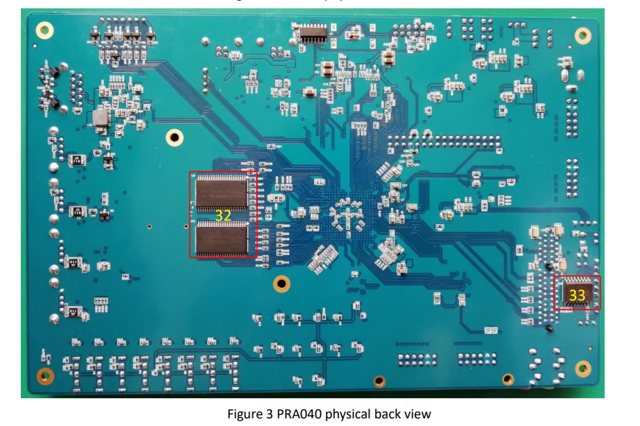
Corresponding to the physical picture, the main devices on board are as follows:
1、10CL040YE484C8G chip
2、External 12V power interface
3、GPIO interface
4、Thermistor (NTC-MF52)
5、Photoresistor
6、Potentiometer
7、Audio output (green), audio input (red)
8、PCIE interface
9、TFTCLD interface
10、Audio chip (WM8978)
11、7 push buttons
12、50M system clock
14、Video chip(ADV7511)
15、External JTAG download interface
16、HDMI interface
17、USB power supply and download interface
18、FPGA and RISC_V JTAG download chips (FT2232)
19、USB_UART interface
20、Serial chip (CP2102)
21、6 7-segment LED display
22、Ethernet interface
23、Ethernet PHY chip (RTL8211E-VB)
24、4 USB interfaces
25、USB mouse and keyboard control chip
26、8 LEDs
27、8-bit DIP switch
28、Reset button
29、Power button
30、Flash (N25Q128A,128M bit/16M bytes)
31、EEPROM (AT24C02N)
32、Two SRAMs
33、AD/DA conversion chip (PCF8591)