FII-PRX100-S FII-PRX100D FPGA Board Based PRX100 Risc-V

Audio 8978 Loopback Experiment – What is I2S (Inter-IC Sound) bus and how it works – AWM8978 Audio Boardudio – Xilinx Risc-V FII-PRX100 Board Experiment 16

Experiment 16 8978 Audio Loopback Experiment

16.1 Experiment Objective

  1. Learn about I2S (Inter-IC Sound) bus and how it works
  2. Familiar with the working mode of WM8978. And by configuring the interface mode and selecting the relevant registers in combination with the development board, complete the data transmission and reception, and verify it

16.2 Experiment Implement

  1. Perform audio loopback test by configuring the onboard audio chip WM8978 to check if the hardware is working properly
  2. Adjust the volume output level with the push buttons.

16.3 Experiment

16.3.1 WM8978 Introduction

WM8978 is a low power, high quality stereo multimedia digital signal CODEC introduced by Wolfson. It is mainly used in portable applications such as digital cameras and camcorders. Advanced on-chip digital signal processing includes a 5-band equaliser, a mixed signal Automatic Level Control for the microphone or line input through the ADC as well as a purely digital limiter function for record or playback. Additional digital filtering options are available in the ADC path, to cater for application filtering, such as “wind noise reduction”.

See Figure 16.1 for the internal structure block diagram of WM8978.

截取-1

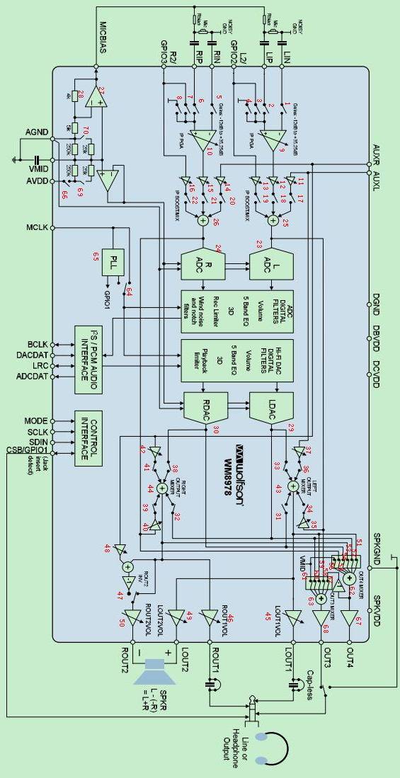
Figure 16.1 WM8978 internal structure block diagram

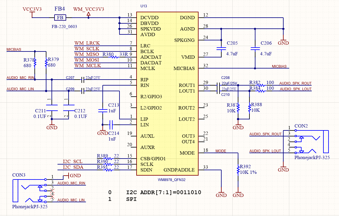
Figure 16.2 Schematics of the audio part of the development board

16.3.2 WM8978 Control Interface Timing

The WM8978 control interface has two-wire mode and three-wire mode. The specific mode is selected by the MODE pin connection of WM8978. When the mode pin is connected to a low voltage level, it is a two-wire mode, and when it is connected to a high voltage level, it is a three-wire mode. The development board mode pin is grounded. When the control interface is in two-wire mode, the timing diagram is shown in Figure 16.3. The timing diagram is the same as the IIC timing. The device address of WM8978 is fixed to 7’b0011010. This chip register only supports writing and does not support reading.

截取-3.jpg

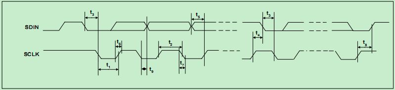
Figure 16.3 Timing diagram of the two-wire mode interface

16.3.3 I2S Audio Bus Protocol

I2S (Inter-IC Sound Bus) is just a branch of PCM, the interface definition is the same, I2S sampling frequency is generally 44.1KHz and 48KHz, PCM sampling frequency is generally 8K, 16K. There are four groups of signals: bit clock signal, synchronization signal, data input, data output.

I2S is a bus standard developed by Philips for audio data transmission between digital audio devices. In the Philips I2S standard, both the hardware interface specification and the format of digital audio data are specified. I2S has three main signals: the serial clock SCLK, also known as the bit clock BCLK, which corresponds to each bit of data of digital audio. The frequency of SCLK = 2 × sampling frequency × sampling number of bits. The frame clock LRCK is used to switch the data of the left and right channels. An LRCK of “0” indicates that data of the left channel is being transmitted, and “1” indicates that data of the right channel is being transmitted. LRCLK == FS, is the sampling frequency serial data SDATA, which is audio data expressed in two’s complement. Sometimes in order to enable better synchronization between systems, another signal MCLK is needed, which is called the master clock, or also called the system Clock (System Clock). It is 256 or 384 times the sampling frequency.

The timing of the I2S protocol is shown in Figure 16.4. However many bits of data the I2S format signal has, the most significant bit of the data always appears at the second BCLK pulse after the LRCK change (that is, the beginning of a frame). This allows the number of significant digits at the receiving end and the transmitting end to be different. If the receiving end can process less significant bits than the transmitting end, the extra low-order data in the data frame can be discarded; if the receiving end can process more significant bits than the transmitting end, it can make up the remaining bits by itself. This synchronization mechanism makes the interconnection of digital audio equipment more convenient without causing data errors.

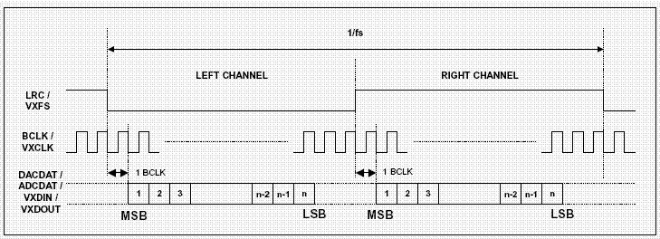
Figure 16.4 I2S timing protocol

16.3.4 Main Program Design

  1. WM8978 register configuration program

Only the program of register configuration program is given here, please refer to the project file for the complete program

1
2
3
4
5
6
7
8
9
10
11
12
13
14
15
16
17
18
19
20
21
22
23
24
25
26
27
28
29
30
31
32
33
34
35
36
37
38
39
40
41
42
43
44
45
46
47
48
49
50
51
52
53
54
55
56
57
58
59
60
61
62
63
64
65
66
67
68
69
70
71
72
73
74
75
76
77
78
79
80
81
82
83
84
85
86
87
88
89
90
91
92
93
94
95
96
97
98
99
100
101
102
103
104
105
106
107
108
109
110
111
112
113
114
115
116
117
118
119
120
121
122
123
124
125
126
127
128
129
130
131
132
133
134
135
136
137
138
139
140
141
142
143
144
145
146
147
148
149
150
151
152
153
154
155
156
157
158
159
160
161
162
163
164
165
166
167
168
169
170
171
172
173
174
175
176
177
178
179
180
181
182
183
184
185
186
187
188
189
190
191
192
193
194
195
196
197
198
199
200
201
202
203
204
205
206
207
208
209
210
211
212
213
214
215
216
217
218
219
220
221
222
223
224
225
226
227
228
229
230
231
232
233
234
235
236
237
238
239
240
241
242
243
244
245
246
247
248
249
250
251
252
253
254
255
256
257
258
259
260
261
262
263
264
265
266
267
268
269
270
271
272
273
274
275
276
277
278
279
280
281
282
283
284
285
286
287
288
289
290
291
292
293
294
295
296
297
298
299
300
301
302
303
304
305
306
307
308
309
310
311
312
313
314
315
316
317
318
319
320
321
322
323
324
325
326
327
328
329
330
331
332
333
334
335
336
337
338
339
340
341
342
343
344
345
346
347
348
349
350
351
352
353
354
355
356
357
358
359
360
361
362
363
364
365
366
367
368
369
370
371
372
373
374
375
376
377
378
379
380
381
382
383
384
385
386
387
388
389
390
391
392
393
394
395
396
397
398
399
400
401
402
403
404
405
406
407
408
409
410
411
412
413
414
415
416
417
418
419
420
421
422
423
424
425
426
427
428
429
430
431
432
433
434
435
436
437
438
439
440
441
442
443
444
445
446
447
448
449
450
451
452
453
454
455
456
457
458
459
460
461
462
463
464
465
466
467
468
469
470
471
472
473
474
475
476
477
478
479
480
481
482
483
484
485
486
487
488
489
490
491
492
493
494
495
496
497
498
499
500
501
502
503
504
505
506
507
508
509
510
511
512
513
514
515
516
517
518
519
520
521
522
523
524
525
526
527
528
529
530
531
532
533
534
535
536
537
538
539
540
541
542
543
544
545
546
547
548
549
550
551
552
553
554
555
556
557
558
559
560
561
562
563
564
565
566
567
568
569
570
571
572
573
574
575
576
577
578
579
580
581
582
583
584
585
586
587
588
589
590
591
592
593
594
595
596
597
module wm8978_config
 
(
 
input clk_50m,
 
output reg cfg_done=0,
 
input rst_n,
 
input rxd,
 
output txd,
 
input key1,
 
input key2,
 
(* mark_debug = "true" *) output i2c_sclk,
 
(* mark_debug = "true" *) inout i2c_sdat
 
);
 
(* mark_debug = "true" *)wire tr_end;
 
(* mark_debug = "true" *)reg [4:0] i;
 
//************************************
 
(* mark_debug = "true" *)reg [23:0] i2c_data_r=0;
 
(* mark_debug = "true" *)wire [7:0] data_read ;
 
(* mark_debug = "true" *)reg [7:0] read_req ;
 
(* mark_debug = "true" *)reg uart_rd =0;
 
(* mark_debug = "true" *)reg uart_wr =0;
 
(* mark_debug = "true" *)reg [7:0] txd_i2c_data;
 
(* mark_debug = "true" *)reg txd_start = 0;
 
wire txd_busy;
 
(* mark_debug = "true" *)wire [7:0] rxd_i2c_data;
 
(* mark_debug = "true" *)wire rxd_ready;
 
(* mark_debug = "true" *)wire rxd_eop;
 
wire test_pin;
 
uart_transceiver uart_transceiver_inst
 
(
 
.sys_clk (clk_50m), // 50m
 
.uart_rx (rxd),
 
.uart_tx (txd),
 
.divisor (55), // 115200 * 8
 
.rx_data (rxd_i2c_data),
 
.rx_done (rxd_ready),
 
.rx_eop (rxd_eop),
 
.tx_data (txd_i2c_data),
 
.tx_wr (txd_start),
 
.tx_done (),
 
.tx_busy (txd_busy),
 
.test_pin (),
 
.sys_rst ()
 
);
 
(* mark_debug = "true" *)reg rx_end_ack = 0;
 
reg rx_end = 0;
 
always @ (posedge clk_50m)
 
if(rxd_eop) rx_end <= 1;
 
else if(rx_end_ack) rx_end <= 0;
 
(* mark_debug = "true" *)reg [7:0] cmd_dir = 0;
 
(* mark_debug = "true" *)reg [3:0] uart_st = 0;
 
always @ (posedge clk_50m)
 
if(cfg_done == 0)
 
begin
 
rx_end_ack <= 0;
 
uart_wr <= 0;
 
uart_rd <= 0;
 
uart_st <= 0;
 
end
 
else case(uart_st)
 
0:
 
begin
 
rx_end_ack <= 0;
 
uart_wr <= 0;
 
uart_rd <= 0;
 
if(rxd_ready)
 
begin
 
cmd_dir <= rxd_i2c_data;
 
uart_st <= 1;
 
end
 
end
 
1:
 
begin
 
if(rxd_ready)
 
begin
 
i2c_data_r[23:16] <= rxd_i2c_data;
 
uart_st <= 2;
 
end
 
end
 
2:
 
begin
 
if(rxd_ready)
 
begin
 
i2c_data_r[15:08] <= rxd_i2c_data;
 
if(cmd_dir[0]) uart_st <= 5;
 
else uart_st <= 3;
 
end
 
end
 
3: // write
 
begin
 
if(rxd_ready)
 
begin
 
i2c_data_r[07:00] <= rxd_i2c_data;
 
uart_wr <= 1;
 
uart_st <= 4;
 
end
 
end
 
4:
 
begin
 
if(tr_end)
 
begin
 
uart_wr <= 0;
 
uart_st <= 7;
 
end
 
end
 
5: //read
 
begin
 
uart_rd <= 1;
 
uart_st <= 6;
 
end
 
6:
 
begin
 
uart_rd <= 0;
 
if(tr_end)
 
begin
 
txd_i2c_data <= data_read;
 
txd_start <= 1;
 
uart_st <= 7;
 
end
 
end
 
7:
 
begin
 
txd_start <= 0;
 
if(rx_end)
 
begin
 
rx_end_ack <= 1;
 
uart_st <= 0;
 
end
 
else rx_end_ack <= 0;
 
end
 
endcase
 
//***************************************
 
reg start;
 
//parameter define
 
reg [5:0] PHONE_VOLUME = 6'd32;
 
reg [5:0] SPEAK_VOLUME = 6'd32;
 
(* mark_debug = "true" *)reg [31:0] i2c_data=0 ;
 
reg [7:0] start_init_cnt;
 
reg [4:0] init_reg_cnt ;
 
reg [25:0] on_counter;
 
reg [25:0] off_counter;
 
(*mark_debug="true"*) reg key_up, key_down;
 
always @(posedge clk_50m , negedge cfg_done)
 
if (!cfg_done) begin
 
on_counter<=0;
 
off_counter<=0;
 
key_up<=1'b0;
 
key_down<=1'b0;
 
end
 
else begin
 
if (key1==1'b1)
 
on_counter<=0;
 
else if ((key1==1'b0)& (on_counter<=500000))
 
on_counter<=on_counter+1'b1;
 
if (on_counter==49950)
 
key_up<=1'b1;
 
else
 
key_up<=1'b0;
 
if (key2==1'b1)
 
off_counter<=0;
 
else if ((key2==1'b0)& (off_counter<=500000))
 
off_counter<=off_counter+1'b1;
 
if (off_counter==49950)
 
key_down<=1'b1;
 
else
 
key_down<=1'b0;
 
end
 
always @(posedge clk_50m , negedge cfg_done)
 
if (!cfg_done) begin
 
PHONE_VOLUME <=6'd32 ;
 
end
 
else begin
 
if (( 2<=PHONE_VOLUME )&( PHONE_VOLUME <=56)&(on_counter==49948))
 
PHONE_VOLUME <=PHONE_VOLUME+6 ;
 
else if (( 8<=SPEAK_VOLUME )&( SPEAK_VOLUME <=62)& (off_counter==49948))
 
PHONE_VOLUME <=PHONE_VOLUME-6 ;
 
else PHONE_VOLUME <=PHONE_VOLUME ;
 
end
 
always @ ( posedge clk_50m )
 
if( rst_n==1'b0 ) begin
 
i <= 5'd0;
 
read_req<=0 ;
 
i2c_data <= 32'h000000;
 
start <= 1'b0;
 
cfg_done <=0;
 
end
 
else begin
 
case( i )
 
0: begin
 
if( tr_end ) begin start <= 1'b00; i <= i + 1'b1; end
 
else begin start <= 1'b1; i2c_data <= {7'h1a,1'b0,8'h00,7'd0 ,9'b1}; end
 
end
 
1: begin
 
if( tr_end ) begin start <= 1'b0; i <= i + 1'b1; end
 
else begin start <= 1'b1; i2c_data <={7'h1a,1'b0, 8'h00,7'd1 ,9'b1_0010_1111}; end
 
end
 
2: begin
 
if( tr_end ) begin start <= 1'b0; i <= i + 1'b1; end
 
else begin start <= 1'b1; i2c_data <= {7'h1a,1'b0,8'h00,7'd2 ,9'b1_1011_0011}; end
 
end
 
3: begin
 
if( tr_end ) begin start <= 1'b0; i <= i + 1'b1; end
 
else begin start <= 1'b1; i2c_data <= {7'h1a,1'b0,8'h00,7'd3 ,9'b0_0110_1111}; end
 
end
 
4: begin
 
if( tr_end ) begin start <= 1'b0; i <= i + 1'b1; end
 
else begin start <= 1'b1; i2c_data <= {7'h1a,1'b0,8'h00,7'd4 ,{2'd0,2'b11,5'b10000}}; end
 
end
 
5: begin
 
if( tr_end ) begin start <= 1'b0; i <= i + 1'b1; end
 
else begin start <= 1'b1; i2c_data <={7'h1a,1'b0,8'h00,7'd6 ,9'b0_0000_0001}; end
 
end
 
6: begin
 
if( tr_end ) begin start <= 2'b00; i <= i + 1'b1; end
 
else begin start <= 1'b1; i2c_data<= {7'h1a,1'b0,8'h00,7'd7 ,9'b0_0000_0001}; end
 
end
 
7: begin
 
if( tr_end ) begin start <= 1'b0; i <= i + 1'b1; end
 
else begin start <= 1'b1; i2c_data <= {7'h1a,1'b0,8'h00,7'd10,9'b0_0000_1000}; end
 
end
 
8: begin
 
if( tr_end ) begin start <= 1'b0; i <= i + 1'b1; end
 
else begin start <= 1'b1; i2c_data <= {7'h1a,1'b0,8'h00,7'd14,9'b1_0000_1000}; end
 
end
 
9: begin
 
if( tr_end ) begin start <= 1'b0; i <= i + 1'b1; end
 
else begin start <= 1'b1; i2c_data <= {7'h1a,1'b0,8'h00,7'd43,9'b0_0001_0000}; end
 
end
 
10: begin
 
if( tr_end ) begin start <= 1'b0; i <= i + 1'b1; end
 
else begin start <= 1'b1; i2c_data <={7'h1a,1'b0,8'h00,7'd47,9'b0_0111_0000}; end
 
end
 
11: begin
 
if( tr_end ) begin start <= 1'b0; i <= i + 1'b1; end
 
else begin start <= 1'b1; i2c_data <={7'h1a,1'b0,8'h00,7'd48,9'b0_0111_0000}; end
 
end
 
12: begin
 
if( tr_end ) begin start <= 1'b0; i <= i + 1'b1; end
 
else begin start <= 1'b1; i2c_data <={7'h1a,1'b0,8'h00,7'd49,9'b0_0000_0110}; end
 
end
 
13: begin
 
if( tr_end ) begin start <= 1'b0; i <= i + 1'b1; end
 
else begin start <= 1'b1; i2c_data <= {7'h1a,1'b0,8'h00,7'd50,9'b1 };end
 
end
 
14: begin
 
if( tr_end ) begin start <= 1'b0; i <= i + 1'b1; end
 
else begin start <= 1'b1; i2c_data <= {7'h1a,1'b0,8'h00,7'd51,9'b1 };end
 
end
 
15: begin
 
if( tr_end ) begin start <= 1'b0; i <= i + 1'b1; end
 
else begin start <= 1'b1; i2c_data <={7'h1a,1'b0,8'h00,7'd52,{3'b010,PHONE_VOLUME}};end
 
end
 
16: begin
 
if( tr_end ) begin start <= 1'b0; i <= i + 1; end
 
else begin start <= 1'b1; i2c_data <= {7'h1a,1'b0,8'h00,7'd53,{3'b110,PHONE_VOLUME}};end
 
end
 
17: begin
 
cfg_done<=1 ;
 
if (uart_wr)
 
begin
 
start <= 1'b1;
 
i2c_data <={cmd_dir,i2c_data_r} ;
 
i<=i+1 ;
 
end
 
if (uart_rd)
 
begin
 
read_req <= 1'b1;
 
i2c_data <={cmd_dir,i2c_data_r} ;
 
i<=i+2 ;
 
end
 
if (key_up|key_down)
 
i<= 15;
 
end
 
18: begin
 
if( tr_end ) begin start <= 1'b0; i <=19; end
 
else i<=20;
 
end
 
19: begin
 
if( tr_end ) begin read_req <= 1'b0; i <= 19; end
 
else begin i<=21;end
 
end
 
default:i<=1 ;
 
endcase
 
end
 
i2c_control i2c_control_inst (
 
.Clk (clk_50m),
 
.Rst_n(rst_n),
 
.wrreg_req(start) ,
 
.rdreg_req (read_req),
 
.addr({i2c_data[15:8],i2c_data[23:16]}) , //16bit
 
.addr_mode(0),
 
.wrdata (i2c_data[7:0]), //
 
.rddata (data_read), //8bit
 
.device_id (i2c_data[31:24]), //8bit
 
.RW_Done(tr_end),
 
.ack (),
 
.i2c_sclk(i2c_sclk),
 
.i2c_sdat(i2c_sdat)
 
);
 
endmodule
  1. Audio signal acquisition program
module audio_receive (

//system clock 50MHz

input rst_n ,

//wm8978 interface

input aud_bclk ,

input aud_lrc ,

input aud_adcdat,

//user interface

output reg rx_done ,

output reg [31:0] adc_data

);

parameter WL = 6’d32 ;

reg aud_lrc_d0;

reg [ 5:0] rx_cnt;

reg [31:0] adc_data_t;

wire lrc_edge ;

assign lrc_edge = aud_lrc ^ aud_lrc_d0;

always @(posedge aud_bclk or negedge rst_n) begin

if(!rst_n)

aud_lrc_d0 <= 1’b0;

else

aud_lrc_d0 <= aud_lrc;

end

always @(posedge aud_bclk or negedge rst_n) begin

if(!rst_n) begin

rx_cnt <= 6’d0;

end

else if(lrc_edge == 1’b1)

rx_cnt <= 6’d0;

else if(rx_cnt < 6’d35)

rx_cnt <= rx_cnt + 1’b1;

end

always @(posedge aud_bclk or negedge rst_n) begin

if(!rst_n) begin

adc_data_t <= 32’b0;

end

else if(rx_cnt < WL)

adc_data_t[WL – 1’d1 – rx_cnt] <= aud_adcdat;

always @(posedge aud_bclk or negedge rst_n) begin

if(!rst_n) begin

rx_done <= 1’b0;

adc_data <= 32’b0;

end

else if(rx_cnt == 6’d32) begin

rx_done <= 1’b1;

adc_data<= adc_data_t;

end

else

rx_done <= 1’b0;

end

endmodule

  1. Audio sending module
module audio_send (

input rst_n ,

input aud_bclk ,

input aud_lrc ,

output reg aud_dacdat,

input [31:0] dac_data ,

output reg tx_done

);

parameter WL = 6’d32 ;

reg aud_lrc_d0;

reg [ 5:0] tx_cnt;

reg [31:0] dac_data_t;

wire lrc_edge;

assign lrc_edge = aud_lrc ^ aud_lrc_d0;

always @(posedge aud_bclk or negedge rst_n) begin

if(!rst_n)

aud_lrc_d0 <= 1’b0;

else

aud_lrc_d0 <= aud_lrc;

end

always @(posedge aud_bclk or negedge rst_n) begin

if(!rst_n) begin

tx_cnt <= 6’d0;

dac_data_t <= 32’d0;

end

else if(lrc_edge == 1’b1) begin

tx_cnt <= 6’d0;

dac_data_t <= dac_data;

end

else if(tx_cnt < 6’d35)

tx_cnt <= tx_cnt + 1’b1;

end

always @(posedge aud_bclk or negedge rst_n) begin

if(!rst_n) begin

tx_done <= 1’b0;

end

else if(tx_cnt == 6’d32)

tx_done <= 1’b1;

else

tx_done <= 1’b0;

end

always @(negedge aud_bclk or negedge rst_n) begin

if(!rst_n) begin

aud_dacdat <= 1’b0;

end

else if(tx_cnt < WL)

aud_dacdat <= dac_data_t[WL – 1’d1 – tx_cnt];

else

aud_dacdat <= 1’b0;

end

endmodule

  1. Main program
module audio_test(

input wire sys_clk_50,

input wire rst_n,

input rxd,

output txd,

output [7:0] led ,

input key1,

input key2,

inout wm_sdin,

output wm_sclk,

input wire wm_lrc,

input wire wm_bclk,

input wire adcdat,

output wire dacdat,

output wire mclk

);

wire sys_clk_50m ;

BUFG BUFG_inst (

.O(sys_clk_50m), // 1-bit output: Clock output

.I(sys_clk_50) // 1-bit input: Clock input

);

wire cfg_done ;

assign led ={7’h7f,~cfg_done} ;

pll_50_12 pll_50_12_inst

(

// Clock out ports

.clk_out_12(clk_out_12), // output clk_out_12

// Status and control signals

.reset(~rst_n), // input reset

.locked(locked), // output locked

// Clock in ports

.sys_clk_50(sys_clk_50m)); // input sys_clk_50

wire clk_out_12 ;

assign mclk = clk_out_12 ;

wm8978_config wm8978_config_inst

(

.key1 (key1),

.key2 (key2),

.clk_50m (sys_clk_50m ) ,

.rst_n (rst_n) ,

.cfg_done (cfg_done) ,

.i2c_sclk (wm_sclk) ,

.rxd (rxd),

.txd (txd),

.i2c_sdat (wm_sdin)

);

wire [31:0] adc_data ;

audio_receive

audio_receive_inst(

.rst_n (rst_n),

.aud_bclk (wm_bclk),

.aud_lrc (wm_lrc),

.aud_adcdat (adcdat),

.adc_data (adc_data),

.rx_done (rx_done)

);

audio_send audio_send_inst(

.rst_n (rst_n),

.aud_bclk (wm_bclk),

.aud_lrc (wm_lrc),

.aud_dacdat (dacdat),

.dac_data (adc_data),

.tx_done (tx_done)

);

endmodule

16.4 Experiment Verification

  1. Pin assignment

Table 16.1 Pin assignment

Signal Name Port Description Network Name FPGA Pin
Sys_clk_50 System 50M clock C10_50MCLK U22
Reset_n System reset signal KEY1 M4
Wm_sdin 8978 register configuration data line I2C_SDA R21
Wm_sclk 8978 register configuration clock I2C_SCL R20
Wm_lrc 8978 align clock WM_LRCK H15
Wm_bclk 8978 bit clock WM_BCLK F18
adcdat ADC input of 8978 WM_MISO G19
Dacdat DAC input of 8978 WM_MOSI F20
Mack PLL provides 8978 working master clock WM_MCLK H17
Key1 Volume up button Key2 L4
Key2 Volume down button Key7 R7
txd Serial transmit TTL_RX L18
rxd Serial receive TTL_TX L17
  1. Board verification

As shown in Figure 16.5 below, after the FPGA development board is programmed, use a dual male audio cable, with one end plugged into the red audio receiver end and the other end plugged into a music player. Plug the headphone into the green audio playback port. The music can be heard from player. The volume is divided into 5 gears. Press the UP key to increase the volume and press the down key to decrease the volume.

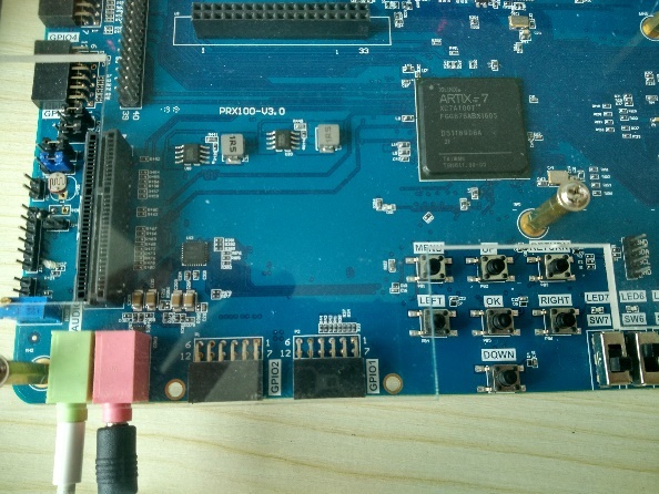
Figure 16.5 wm8978 board verification

Visited 1 times, 1 visit(s) today

Related posts