Reading Experiment of Serial Port Partition of Static Memory SRAM, Read and write timing of IS61WV25616BLL SRAM, and prepare for the next experimental experiment of OV5640 camera experiment – – Xilinx Risc-V FII-PRX100 Board Experiment 17
Experiment 17 Reading Experiment of Serial Port Partition of Static Memory SRAM
17.1 Experiment Objective
- Learn about static memory SRAM read and write operations and how it works
- Familiar with the read and write timing of IS61WV25616BLL SRAM, and prepare for the next experimental experiment of OV5640 camera experiment.
17.2 Experiment Implement
- The experimental board is equipped with two pieces of SRAM, which are combined to form 18-bit address lines and 32-bit data spaces. After power-on, the FPGA will write the same value in the corresponding address in the entire memory space.
- The base address value of the SRAM is read and issued through the serial port, and then the stored data value corresponding to the base value space will be sent to the host computer through the serial port for display (the value corresponding to each base value interval).
17.3 Experiment
17.3.1 SRAM Introduction
SRAM (Static Random-Access Memory) is a type of random access memory. The “static” means that as long as the power is on, the data in the SRAM will remain unchanged. However, the data will still be lost after power turned off, which is the characteristics of the RAM.
Two SRAMs (IS61WV25616BLL) are on the development board, each SRAM has 256 * 16 words of storage space. Each word is 16-bit. The maximum read and write speed can reach 100 MHz. The physical picture is shown in Figure 17.1.
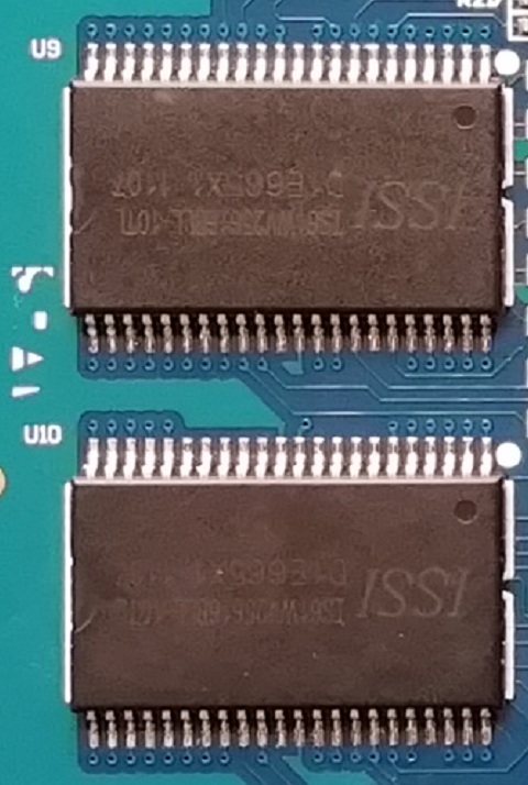
Figure 17.1 SRAM physical picture
17.3.2 Schematics
The schematics of the development board is shown in Figure 17.2: two pieces of SRAM share the same set of address lines to form a memory space with a bit width of 32 and a depth of 18 bits.
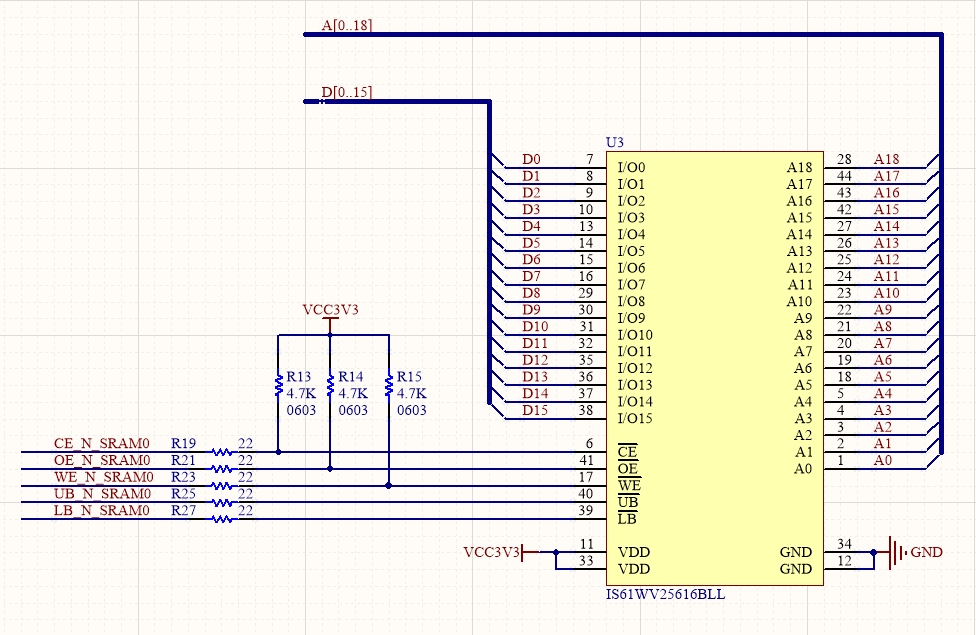
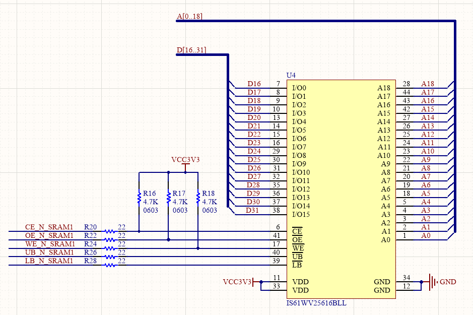
Figure 17.2 Schematics of SRAM0 and SRAM1
17.3.3 Main Program Design
The content of the serial port has been described before, and the core program is as follows:
- Sram controller design
From the official manual, there are two types of read timing for SRAM. The first read timing is used here as shown in Figure 17.3. Reading data is controlled by the Address bus
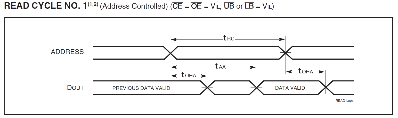
Figure 17.3 SRAM read timing
There are four types of write timing. The write timing used here is shown in Figure 17.4. The write control is controlled by the WE signal line.
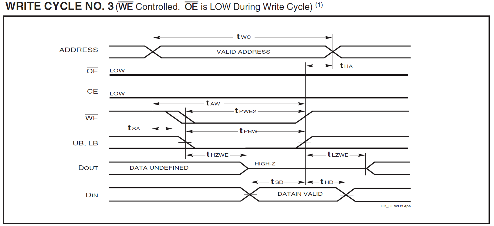
Figure 17.4 SRAM write timing
The program is as follows:
| module sram_ctr (
input wire clk_50, input wire rst_n , input wire wr_en, input wire rd_en, input wire [17:0] sram_addr_wr_rd, input wire [31:0] data_we , output reg [31:0] data_rd, output reg data_valid=0 , output reg [17:0] sram_addr, inout [31:0] sram_data, output reg sram1_ce, output reg sram1_oe, output reg sram1_we, output reg sram1_lb, output reg sram1_ub, output reg sram0_ce, output reg sram0_oe, output reg sram0_we, output reg sram0_lb, output reg sram0_ub ) ; reg out_link=0; reg [31:0] sram_data_r; assign sram_data = out_link ? sram_data_r : 32’bz ; reg [1:0] sram_st=2’d0; always @ (posedge clk_50) begin if (~rst_n) begin sram_st <=2’d0; sram1_ce <=0; sram1_oe <=0; sram1_we <=1; sram1_lb <=0; sram1_ub <=0; sram0_ce <=0; sram0_oe <=0; sram0_we <=1; sram0_lb <=0; sram0_ub <=0; data_valid<=0 ; end else begin case (sram_st) 0 :begin sram1_ce <=0 ; sram1_oe <=0 ; sram1_we <=1 ; sram1_lb <=0 ; sram1_ub <=0 ; sram0_ce <=0 ; sram0_oe <=0 ; sram0_we <=1 ; sram0_lb <=0 ; sram0_ub <=0 ; data_valid<=0 ; sram_st<=1 ; end 1 : begin data_rd<=sram_data; data_valid<=0 ; out_link <=0 ; if (wr_en) begin sram1_we<=0; sram0_we<=0; sram_addr<=sram_addr_wr_rd; sram_data_r<= data_we ; out_link <=1 ; sram_st<=2 ; end if (rd_en) begin out_link <=0 ; sram1_we <=1; sram0_we <=1; sram_st<=3 ; sram_addr<=sram_addr_wr_rd; data_rd<=sram_data; end end 2 : begin sram1_we <=1; sram0_we <=1; sram_addr<=sram_addr_wr_rd; data_rd<=sram_data; sram_st<=1 ; end 3 : begin sram_addr<=sram_addr_wr_rd; data_rd<=sram_data; data_valid<=1 ; if (~rd_en) sram_st<=1; end default : sram_st<=0; endcase end end endmodule |
SRAM write data and read data program design: After the board is programmed, it will automatically write the value corresponding to the address from 0 to 18’h3ffff. The serial program issues the base address for reading the sram. All the data stored in the corresponding base address range will be returned and sent to the host computer through the serial port for display. (Here SRAM is divided into 8’h00 to 8’h3f base address spaces)
| module data_gen(
input wire sys_clk, input wire data_valid_rd , input wire rst_n, input wire rd_cmd, input wire [7:0] rd_cmd_addr, input tx_done , input [31:0] sramrd_data , output reg led =1, output [7:0] dout , output valid, output reg sram_rd_req, output reg sram_we_req , output reg [31:0] sram_data_we, output [17:0] sram_addr_we_rd ); reg rd_sign=0 ; reg [17:0] sram_addr_rd =0; reg [17:0] sram_addr_we =0 ; assign sram_addr_we_rd =led ?sram_addr_we: sram_addr_rd ; reg [18:0] wcnt; always @(posedge sys_clk) if (!rst_n)led<=1; else if (wcnt==19’h7FFFF) led<=0; else led<=led; always @ (posedge sys_clk,negedge rst_n) if (!rst_n) wcnt<=19’d0 ; else begin if (led) wcnt<=wcnt+1 ; else wcnt<=wcnt; end always @ (posedge sys_clk,negedge rst_n) if (!rst_n) begin sram_we_req <= 0 ; sram_data_we <=32’d0 ; sram_addr_we <=18’d0 ; end else begin if (led) begin if (!wcnt[0]) begin sram_we_req <= 1 ; sram_data_we <=sram_data_we ; sram_addr_we <=sram_addr_we ; end else begin sram_we_req <= 0 ; sram_data_we <=sram_data_we+1 ; sram_addr_we <=sram_addr_we +1; end end else begin sram_we_req <= 0 ; sram_data_we <=0 ; sram_addr_we <=0; end end reg [11:0] rdcnt =12’hfff; always @ (posedge sys_clk ,negedge rst_n) if (!rst_n) begin rdcnt<=12’hfff; sram_addr_rd <=18’d0 ; sram_rd_req <=0 ; rd_sign<=0 ; end else begin if(led==0) begin if (rd_cmd) begin rdcnt<=12’h000; sram_addr_rd<={rd_cmd_addr [5:0],12’h000}; sram_rd_req <=1 ; rd_sign<=1 ; end else begin if (rdcnt<12’hfff) begin rdcnt<=rdcnt+1; sram_addr_rd<=sram_addr_rd+1 ;end else begin rdcnt<=rdcnt;rd_sign<=0 ;if(rd_sign==0) sram_rd_req <=0 ; end end end else rdcnt<=12’hfff; end reg rd_en =0 ; wire [14 : 0] rd_data_count ; reg [1:0] cnt_cs =0 ; always @ (posedge sys_clk,negedge rst_n) if (!rst_n) begin rd_en <=0 ; cnt_cs<=2’b00 ; end else begin case (cnt_cs) 0: begin rd_en <=0 ; cnt_cs<=1 ; end 1: begin if (rd_data_count) begin rd_en <=1 ; cnt_cs<=2 ; end else begin rd_en <=0 ; cnt_cs<=1 ; end end 2: begin rd_en <=0 ; cnt_cs<=3 ; end 3: begin rd_en <=0 ; if (tx_done) cnt_cs<=0 ; else cnt_cs<=3 ; end endcase end fifo_sram your_instance_name ( .rst(!rst_n), // input wire rst .wr_clk(sys_clk), // input wire wr_clk .rd_clk(sys_clk), // input wire rd_clk .din(sramrd_data), // input wire [31 : 0] din .wr_en(data_valid_rd), // input wire wr_en .rd_en(rd_en), // input wire rd_en .dout(dout), // output wire [7 : 0] dout .full(), // output wire full .empty(empty), // output wire empty .valid(valid), // output wire valid .rd_data_count(rd_data_count), // output wire [14 : 0] rd_data_count .wr_rst_busy(), // output wire wr_rst_busy .rd_rst_busy() // output wire rd_rst_busy ); endmodule |
17.4 Board Verification
1 Pin assignment
Table 17.1 SRAM pin mapping
| Signal Name | Port Description | Network Name | FPGA Pin |
| Clk_50m | 50M system clock | C10_50MCLK | U22 |
| Sys_rst_n | System reset | KEY1 | M4 |
| Uart_rx | Serial receive | TTL_TX | L17 |
| Uart_tx | Serial transmit | TTL_RX | L18 |
| Sram_data[0] | SRAM data bus | D0 | U21 |
| Sram_data[1] | SRAM data bus | D1 | U25 |
| Sram_data[2] | SRAM data bus | D2 | W26 |
| Sram_data[3] | SRAM data bus | D3 | Y26 |
| Sram_data[4] | SRAM data bus | D4 | AA25 |
| Sram_data[5] | SRAM data bus | D5 | AB26 |
| Sram_data[6] | SRAM data bus | D6 | AA24 |
| Sram_data[7] | SRAM data bus | D7 | AB24 |
| Sram_data[8] | SRAM data bus | D8 | AC24 |
| Sram_data[9] | SRAM data bus | D9 | AC26 |
| Sram_data[10] | SRAM data bus | D10 | AB25 |
| Sram_data[11] | SRAM data bus | D11 | Y23 |
| Sram_data[12] | SRAM data bus | D12 | Y25 |
| Sram_data[13] | SRAM data bus | D13 | W25 |
| Sram_data[14] | SRAM data bus | D14 | V26 |
| Sram_data[15] | SRAM data bus | D15 | U26 |
| Sram_data[16] | SRAM data bus | D16 | T14 |
| Sram_data[17] | SRAM data bus | D17 | T17 |
| Sram_data[18] | SRAM data bus | D18 | W18 |
| Sram_data[19] | SRAM data bus | D19 | U17 |
| Sram_data[20] | SRAM data bus | D20 | V18 |
| Sram_data[21] | SRAM data bus | D21 | T18 |
| Sram_data[22] | SRAM data bus | D22 | W19 |
| Sram_data[23] | SRAM data bus | D23 | T19 |
| Sram_data[24] | SRAM data bus | D24 | W21 |
| Sram_data[25] | SRAM data bus | D25 | Y22 |
| Sram_data[26] | SRAM data bus | D26 | Y21 |
| Sram_data[27] | SRAM data bus | D27 | U20 |
| Sram_data[28] | SRAM data bus | D28 | T20 |
| Sram_data[29] | SRAM data bus | D29 | W20 |
| Sram_data[30] | SRAM data bus | D30 | Y20 |
| Sram_data[31] | SRAM data bus | D31 | V19 |
| Sram_addr[0] | SRAM address bus | A0 | E26 |
| Sram_addr[1] | SRAM address bus | A 1 | E25 |
| Sram_addr[2] | SRAM address bus | A 2 | D26 |
| Sram_addr[3] | SRAM address bus | A 3 | D25 |
| Sram_addr[4] | SRAM address bus | A 4 | G22 |
| Sram_addr[5] | SRAM address bus | A 5 | H18 |
| Sram_addr[6] | SRAM address bus | A 6 | M15 |
| Sram_addr[7] | SRAM address bus | A 7 | M16 |
| Sram_addr[8] | SRAM address bus | A 8 | L15 |
| Sram_addr[9] | SRAM address bus | A 9 | K23 |
| Sram_addr[10] | SRAM address bus | A 10 | J25 |
| Sram_addr[11] | SRAM address bus | A 11 | K22 |
| Sram_addr[12] | SRAM address bus | A 12 | H26 |
| Sram_addr[13] | SRAM address bus | A 13 | J26 |
| Sram_addr[14] | SRAM address bus | A 14 | J24 |
| Sram_addr[15] | SRAM address bus | A 15 | G25 |
| Sram_addr[16] | SRAM address bus | A 16 | G24 |
| Sram_addr[17] | SRAM address bus | A 17 | J21 |
| Sram_addr[18] | SRAM address bus | A 18 (invalid pin) | J23 |
| Sram0_cs_n | 0th SRAM enable | CE_N_SRAM0 | F25 |
| Sram0_we_n | 0th SRAM write enable | OE_N_SRAM0 | L19 |
| Sram0_oe_n | 0th SRAM read enable | WE_N_SRAM0 | H23 |
| Sram0_ub_n | 0th SRAM high byte enable | UE_N_SRAM0 | H24 |
| Sram0_lb_n | 0th SRAM low byte enable | LE_N_SRAM0 | G26 |
| Sram0_cs_n | 1st SRAM enable | CE_N_SRAM1 | E23 |
| Sram0_we_n | 1st SRAM write enable | OE_N_SRAM1 | J18 |
| Sram0_oe_n | 1st SRAM read enable | WE_N_SRAM1 | F23 |
| Sram0_ub_n | 1st SRAM high byte enable | UE_N_SRAM1 | F24 |
| Sram0_lb_n | 1st SRAM low byte enable | LE_N_SRAM1 | K20 |
2 Board Verification
After the FPGA development board is programmed. When led0 is on, it indicates that the program’s write operation to the SRAM is complete, and the SRAM can be read through the serial port. Serial port parameter setting: Baud rate: 9600, no parity. The following figure 17.4 shows the display result of the host computer reading the base address 8’h3f (base address range 8’h00 ~ 8’h3f). The data read out is one group per 4 bits. The green box is as follows: 0003F000, where 3F is the corresponding input base address. The next 3 digits are from 000 to FFF. The reception shows that the number of 2 to the power 12 times 4, which is equal to 16384. It indicates that the number of data read back is correct.
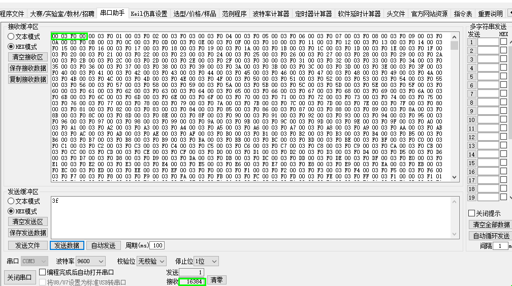
Figure 17.4 Result of reading the SRAM base address range by the serial port