Altera Risc-V FPGA Tutorial : Hexadecimal Number to BCD Code Conversion and Application – FII-PRA040 FPGA Board Experimental 7
Experiment 7 Hexadecimal Number to BCD Code Conversion and Application
Experiment Objective
- Learn to convert binary numbers to BCD code (bin_to_bcd)
- Learn to convert hexadecimal numbers to BCD code (hex_to_bcd)
7.2 Experimental Implement
Combined with experiment 6, display the results of the operation to the segment display.
7.3 Experiment
7.2.1 Introduction to the principle of hexadecimal number to BCD code
Since the hexadecimal display is not intuitive, decimal display is more widely used in real life.
Human eyes recognition is relatively slow, so the display from hexadecimal to decimal does not need to be too fast. Generally, there are two methods
- Countdown method:
Under the control of the synchronous clock, the hexadecimal number is decremented by 1 until it is reduced to 0. At the same time, the appropriate BCD code decimal counter is designed to increment. When the hexadecimal number is reduced to 0, the BCD counter Just gets with the same value to display.
- Bitwise operations (specifically, shift bits and plus 3 here). The implementation is as follows:
- Set the maximum decimal value of the expression. Suppose you want to convert the 16-digit binary value (4-digit hexadecimal) to decimal. The maximum value can be expressed as 65535. First define five four-digit binary units: ten thousand, thousand, hundred, ten, and one to accommodate calculation results
- Shift the hexadecimal number by one to the left, and put the removed part into the defined variable, and judge whether the units of ten thousand, thousand, hundred, ten, and one are greater than or equal to 5, and if so, add the corresponding bit to 3 until the 16-bit shift is completed, and the corresponding result is obtained.
Note: Do not add 3 when moving to the last digit, put the operation result directly
- The principle of hexadecimal number to BCD number conversion
Suppose ABCD is a 4-digit binary number (possibly ones, 10 or 100 bits, etc.), adjusts it to BCD code. Since the entire calculation is implemented in successive shifts, ABCDE is obtained after shifting one bit (E is from low displacement and its value is either 0 or 1). At this time, it should be judged whether the value is greater than or equal to 10. If so, the value is increased by 6 to adjust it to within 10, and the carry is shifted to the upper 4-bit BCD code. Here, the pre-movement adjustment is used to first determine whether ABCD is greater than or equal to 5 (half of 10), and if it is greater than 5, add 3 (half of 6) and then shift.
For example, ABCD = 0110 (decimal 6)
- After shifting it becomes 1100 (12), greater than 1001 (decimal 9)
- By plus 0110 (decimal 6), ABCD = 0010, carry position is 1, the result is expressed as decimal 12
- Use pre-shift processing, ABCD = 0110 (6), greater than 5, plus 3
- ABCD = 1001 (9), shift left by one
- ABCD = 0010, the shifted bit is the lowest bit of the high four-bit BCD.
- Since the shifted bit is 1, ABCD = 0010(2), the result is also 12 in decimal.
- The two results are the same
- Firstly, make a judgement, and then add 3 and shift. If there are multiple BCD codes at the same time, then multiple BCD numbers all must first determine whether need to add 2 and then shift.
- The first way is relatively easy. Here, the second method is mainly introduced.
Example 1: Binary to BCD. See Figure 7.1.
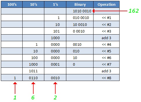
Figure 7.1 Example 1, bin_to_bcd
Example 2: Hexadecimal to BCD. See Figure 7.2.
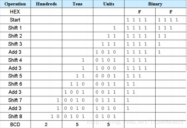
Figure 7.2 hex_to_bcd
7.2.2 Introduction to the Program
The first step: the establishment of the main program framework
| module HEX_BCD (
input [15:0] hex, output reg [3:0] ones, output reg [3:0] tens, output reg [3:0] hundreds, output reg [3:0] thousands, output reg [3:0] ten_thousands ); |
Enter a 16-bit binary number hex, which can represent a maximum of 65535 decimal, so output ones, tens, hundreds, thousands, and ten_thousands.
The second step: the implementation of bit operation
| reg [15:0] hex_reg;
integer i; always @ (*) begin hex_reg = hex; ones = 0; tens = 0; hundreds = 0; thousands = 0; ten_thousands = 0;
for (i = 15; i >= 0; i = i-1) begin if(ten_thousands >= 5) ten_thousands = ten_thousands + 3; if(thousands >= 5) thousands = thousands + 3; if(hundreds >= 5) hundreds = hundreds + 3; if(tens >= 5) tens = tens + 3; if(ones >= 5) ones = ones + 3; ten_thousands = ten_thousands << 1; ten_thousands[0] = thousands[3]; thousands = thousands << 1; thousands[0] = hundreds[3]; hundreds = hundreds << 1; hundreds[0] = tens[3]; tens = tens << 1; tens[0]= ones[3]; ones = ones << 1; ones[0] = hex_reg[15]; hex_reg = {hex_reg[14:0], 1’b0}; end end |
Referring to Figure 7.2, the former part of the program is the judgment calculation part, and if it is greater than or equal to 5, then adds 3. The latter part is the shift part.
The third step: verification
Referring to Experiment 6, simulation was performed using ModelSim, and the simulation conditions were set as follows:
| initial begin
hex = 0 ; repeat (20) begin #10; hex = {$random}%20000; #10; end end |
At the beginning, the 16-bit binary number is equal to 0. The delay is 10 ns. The 16-bit binary number takes a random number less than 20,000. A delay of 10 ns is applied and the process is repeated 20 times.
After the ModelSim is set and the testbench file is added, perform the simulation. The result is shown in Figure 7.3.
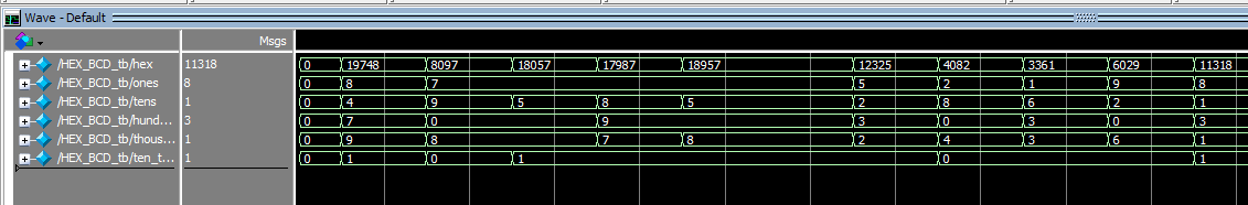
Figure 7.3 Simulation for binary to decimal
Remark and reflection:
- The assignment marks for the examples above are “=” instead of “<=”. Why?
- Since the whole program is designed to be combinational logic, when invoking the modules, the other modules should be synchronized the timing.
7.4 Application of Hexadecimal Number to BCD Number Conversion
- Continue to complete the multiplier of Experiment 6 and display the result in segment display in decimal. Every 1 second, the calculation result on the segment display changes once. The experiment needs to use frequency division, segment display, multiplier and hexadecimal number to BCD code.
- Compilation. Observe the Timing Analyzer in Compilation Report.
- Fmax Summary 83.71 MHz. See Figure 7.4.
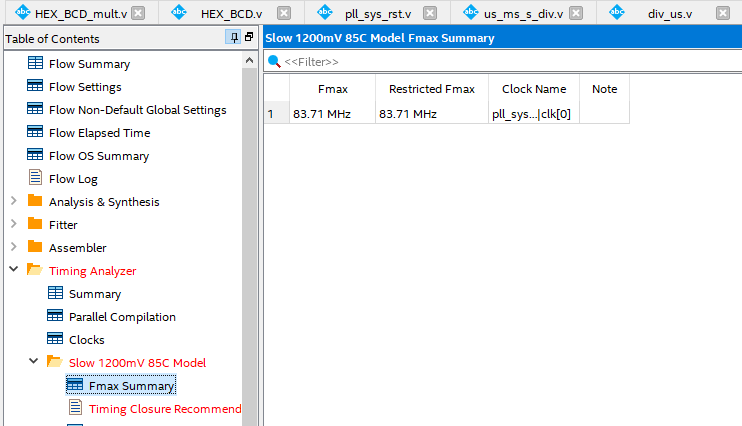
Figure 7.4 Fmax Summary
- Setup Memory
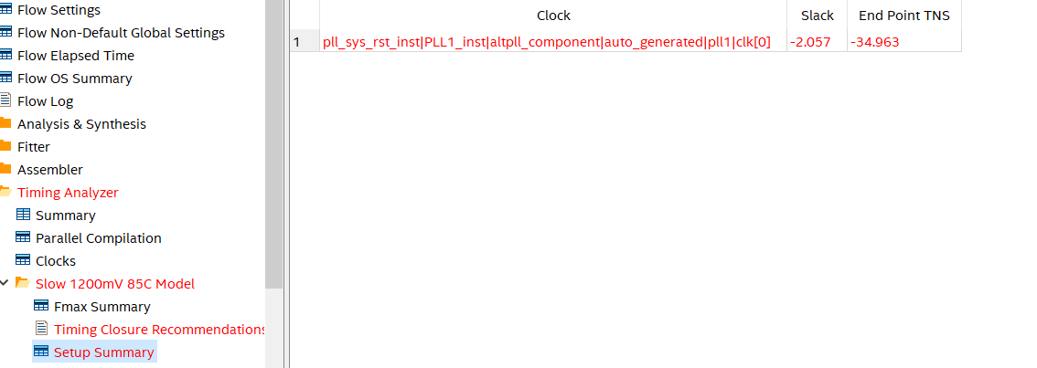
Figure 7.5 Setup time summary
- Timing Closure Recommendation. See Figure 7.6.
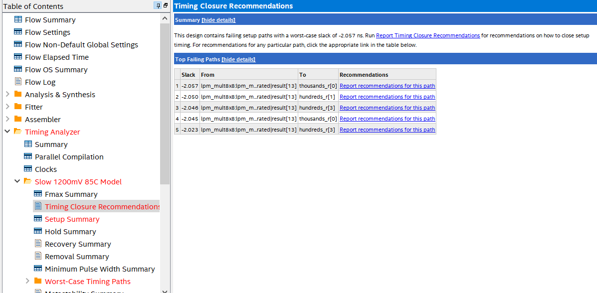
Figure 7.6 Timing Analysis
- From the above three indicators, the above programming does not meet the timing requirements. It can also be seen that the maximum delay path is the delay of the output of the multiplier to HEX_BCD.
There are 3 solutions:
- Reduce the clock frequency
- Increase the timing of HEX_BCD and increase the pipeline
- Insert pipeline isolation at the periphery (can reduce some delay)
The way to increase the pipeline, will be introduced in the follow-up experiment, because the function of HEX_BCD is mainly used to display the human-machine interface, the speed requirement is low, and the frequency reduction method is adopted here.
- Modify PLL to increase an output of 20 MHz frequency (BCD_clk)..
- Recompile and observe timing results
- Lock the pins, compile, and download the programto FII-PRA040 development board for testing
7.5 Experiment Verification
The first step: pin assignment
Table 7.1 Hexadecimal number to BCD pin mapping
| Signal Name | Network Label | FPGA Pin | Description |
| clk | CLK_50M | G21 | Input clock |
| rst_n | PB3 | Y6 | Reset |
| scan[0] | SEG_3V3_D5 | F14 | Bit selection 0 |
| scan[1] | SEG_3V3_D4 | D19 | Bit selection 1 |
| scan[2] | SEG_3V3_D3 | E15 | Bit selection 2 |
| scan[3] | SEG_3V3_D2 | E13 | Bit selection 3 |
| scan[4] | SEG_3V3_D1 | F11 | Bit selection 4 |
| scan[5] | SEG_3V3_D0 | E12 | Bit selection 5 |
| seven_seg[0] | SEG_PA | B15 | Segment a |
| seven_seg[1] | SEG_PB | E14 | Segment b |
| seven_seg[2] | SEG_PC | D15 | Segment c |
| seven_seg[3] | SEG_PD | C15 | Segment d |
| seven_seg[4] | SEG_PE | F13 | Segment e |
| seven_seg[5] | SEG_PF | E11 | Segment f |
| seven_seg[6] | SEG_PG | B16 | Segment g |
| seven_seg[7] | SEG_DP | A16 | Segment h |
| SW[7] | PB7 | W6 | Swicth 7 |
| SW[6] | PB6 | Y8 | Swicth 6 |
| SW[5] | PB5 | W8 | Swicth 5 |
| SW[4] | PB4 | V9 | Swicth 4 |
| SW[3] | PB3 | V10 | Swicth 3 |
| SW[2] | PB2 | U10 | Swicth 2 |
| SW[1] | PB1 | V11 | Swicth 1 |
| SW[0] | PB0 | U11 | Swicth 0 |
Step 2: board downloading verification
After the pin assignment is completed, the compilation is performed. Downloading program to the board is verified after passing. The experimental result is shown in Figure 7.7. The value of the DIP switch input is 00001010, the decimal is 10, the counter is constantly accumulating, so the display result is always accumulatively changed by 10.
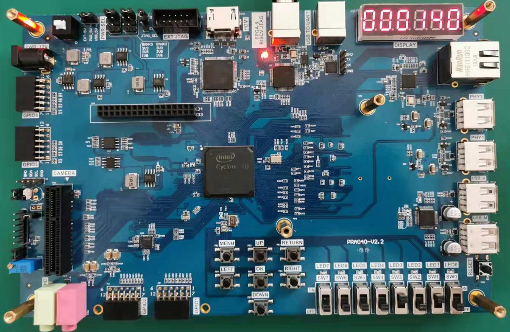
Figure 7.7 Experiment result
Experiment Summary and Reflection
- How to implement BCD using more than 16bits binary numbers
- What is a synchronous clock and how to handle an asynchronous clock
- Learn to design circuits meeting the requirement