Xilinx Risc-V Board Tutorial : Block/SCH Digital Clock Design- FII-PRX100 FPGA Board Experiment 4
Experiment 4 Block/SCH Digital Clock Design
1.Experiment Objective
-
- Review the new FPGA project building in Vivado, device selection, PLL creation, PLL frequency setting, Verilog tree hierarchy design, and the use of ILA
- Master the design method of graphics from top to bottom
- Combine the BCD_counter project to realize the movement of the decimal point (DP) of the decoder
- Observe the test result
2.Experiment Procedure
- File -> Project -> New
Select Device: XC7A100T-2FGG676I
- See Fig 4. 1, add source file, new top-level entity: block_counter.v
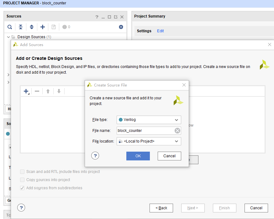
Fig 4. 1 Build source file
- As shown in Fig 4. 2, add the PLL as in the experiment 1, set the input clock to 50 MHz, and the output clock to 100 MHz.
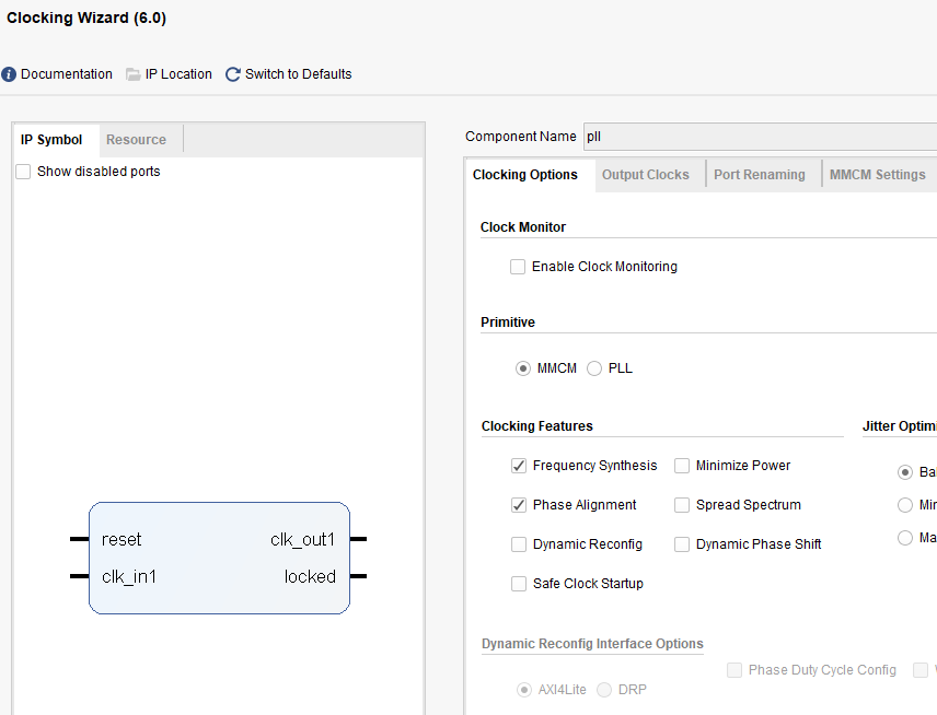
Fig 4. 2 Set the PLL IP core
- Create a new Verilog HDL file for the frequency divider
- Divide the 100 MHz clock into a 1 MHz clock
| module div_us(
input rst, input sys_clk, output reg us_f ); reg[6:0] us_r; always@(posedge sys_clk) if(rst)begin us_r<=0; us_f<=1’b0; end else begin us_f<=1’b0; if(us_r==99)begin us_r<=0; us_f<=1’b1; end else begin us_r<=us_r+1; end end endmodule |
-
- Create a new 1000 division verilog HDL file again, div_1000f.v
| module div_1000f
( input rst, input sys_clk, input in_f, output reg div1000_f ); reg[9:0] div1000_r; always@(posedge sys_clk) if(rst)begin div1000_r<=9’d0; div1000_f<=1’b0; end else begin div1000_f<=1’b0; if(in_f) begin if(div1000_r==999)begin div1000_r<=0; div1000_f<=1’b1; end else begin div1000_r<=div1000_r+1; end end end endmodule |
- Use the 1000 frequency division program div_1000f.v to divide the 1 MHZ clock into 1000 HZ, 1 HZ clock.
| module block_dvi(
input wire sys_clk, input wire sys_rst,
output wire us_f, output wire ms_f, output wire s_f );
div_us div_us_inst( .rst (sys_rst), .sys_clk (sys_clk) , .us_f (us_f) );
div_1000f div_1000f_inst( .rst (sys_rst) , .sys_clk (sys_clk) , .in_f (us_f ) , .div1000_f (ms_f) );
div_1000f div_1000f_inst2( .rst (sys_rst) , .sys_clk (sys_clk) , .in_f (ms_f ) , .div1000_f (s_f) );
endmodule |
- Create a new Verilog file bcd_counter.v, design hour counter and minute counter
| module bcd_counter(
input rst, input sys_rst, input sys_clk, input ms_f, input s_f, output reg [7:0] seven_seg, output reg [3:0] scan ); reg ext_rst; reg min_f;
reg [3:0] counta,countb; reg [3:0] countc,countd; reg [3:0] count_sel;
reg [6:0]seven_seg_r;
always@(posedge sys_clk) begin ext_rst<=sys_rst; end
always@(posedge sys_clk) if(ext_rst)begin counta<=0; countb<=0; min_f <=1’b0; end else begin min_f <=1’b0; if(s_f) begin if(counta==4’d9) begin counta<=4’d0; if(countb==5)begin countb<=0; min_f<=1’b1; end else countb<=countb+1’b1; end else begin counta<=counta+1’b1; end end
end always@(posedge sys_clk) if(ext_rst)begin countc<=4’d0; countd<=4’d0; end else begin if(min_f) begin if(countc==4’d9) begin countc<=4’d0; if(countd==5)begin countd<=0; end else countd<=countd+1’b1; end else begin countc<=countc+1’b1; end end
end
reg [1:0] scan_st;
always@(posedge sys_clk) if(ext_rst) begin scan <=4’b1111; count_sel <=4’d0; scan_st<=0; end else case(scan_st) 0:begin scan <=4’b1110; count_sel <=counta; if(ms_f) scan_st <=1; end 1:begin scan <=4’b1101; count_sel <=countb; if(ms_f) scan_st <=2; end 2:begin scan<=4’b1011; count_sel <=countc; if(ms_f) scan_st<=3; end 3:begin scan<=4’b0111; count_sel <=countd; if(ms_f) scan_st<=0; end default:scan_st<=0; endcase
always@(*) case(count_sel) 0:seven_seg_r<=7’b100_0000; 1:seven_seg_r<=7’b111_1001; 2:seven_seg_r<=7’b010_0100; 3:seven_seg_r<=7’b011_0000; 4:seven_seg_r<=7’b001_1001; 5:seven_seg_r<=7’b001_0010; 6:seven_seg_r<=7’b000_0011; 7:seven_seg_r<=7’b111_1000; 8:seven_seg_r<=7’b000_0000; 9:seven_seg_r<=7’b001_0000; default:seven_seg_r<=7’b100_0000; endcase always@(posedge sys_clk) seven_seg<={1’b1,seven_seg_r};
endmodule |
- Instantiate each function module subroutine into the top-level entity for comprehensive compilation.
| module block_counter(
input wire rst, input wire clk_in,
output wire [7:0] seven_seg, output wire [3:0] scan );
wire us_f; wire ms_f ; wire s_f ;
reg sys_rst; wire sys_clk;
block_dvi block_dvi_inst( .sys_clk (sys_clk) , .sys_rst (sys_rst) , .us_f (us_f) , .ms_f (ms_f) , .s_f (s_f) ); always @(posedge sys_clk) sys_rst <=!locked ; pll pll_inst ( // Clock out ports .clk_out1(sys_clk), // output clk_out1 // Status and control signals .reset(1’b0), // input reset .locked(locked), // output locked // Clock in ports .clk_in1(clk_in)); // input clk_in1
bcd_counter bcd_counter_inst( .rst (rst) , .sys_rst (sys_rst) , .sys_clk (sys_clk) , //c0_50Mclk .ms_f (ms_f) , .s_f (s_f) , .seven_seg (seven_seg) , .scan (scan) ); endmodule |
- Lock the Pin
| Signal Name | Port Description | Network Label | FPGA Pin |
| inclk_in | Sytem clock 50 MHz | C10_50MCLK | U22 |
| rst | Reset, high by default | KEY1 | M4 |
| seven_seg[0] | Segment a | SEG_PA | K26 |
| seven_seg[1] | Segment b | SEG_PB | M20 |
| seven_seg[2] | Segment c | SEG_PC | L20 |
| seven_seg[3] | Segment d | SEG_PD | N21 |
| seven_seg[4] | Segment e | SEG_PE | N22 |
| seven_seg[5] | Segment f | SEG_PF | P21 |
| seven_seg[6] | Segment g | SEG_PG | P23 |
| seven_seg[7] | Segment h | SEG_DP | P24 |
| scan[0] | Segment 6 | SEG_3V3_D5 | T24 |
| scan[1] | Segment 5 | SEG_3V3_D4 | R25 |
| scan[2] | Segment 4 | SEG_3V3_D3 | K25 |
| scan[3] | Segment 3 | SEG_3V3_D2 | N18 |
- Compile, download to the board and test the program. The test result is shown in Fig 4. 3.
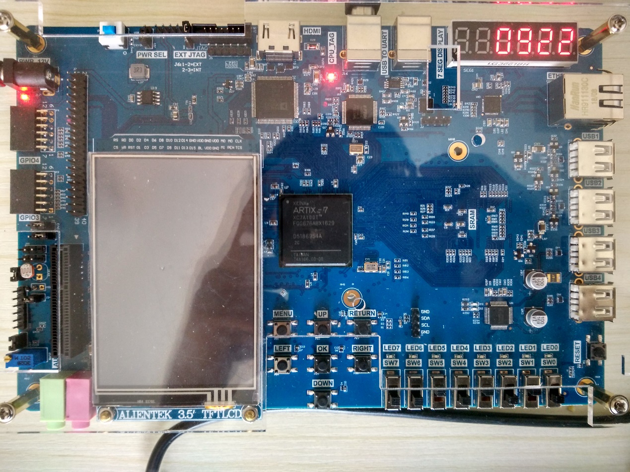
Fig 4. 3 Test result
3.More to Practice
-
-
- Practice the design of high-level digital clocks, month (positional system by base 30), day (positional system by base 24), hour (sexagesimal), and minute (sexagesimal).
- The content of this lab exercise is to use the design with a top-down design approach.
-