FII-PE7030 Hardware Reference Guide
V1.1
Fraser innovation inc
FII-PE7030 Hardware Reference Guide
Version Control
| Version | Date | Description |
| V1.0 | 08/27/2019 | Initial Release |
| V1.1 | 11/19/2019 | Add some SD Card Part and Potentiometer Part |
Copyright Notice:
© 2019 Fraser Innovation Inc ALL RIGHTS RESERVED
Without written permission of Fraser Innovation Inc, no unit or individual may extract or modify part of or all the contents of this manual. Offenders will be held liable for their legal responsibility.
Thank you for purchasing the FPGA development board. Please read the manual carefully before using the product and make sure that you know how to use the product correctly. Improper operation may damage the development board. This manual is constantly updated, and it is recommended that you download the latest version when using.
Contents
7)Gigabit Ethernet Interface 21
11)FMC-LPC High-speed Interface 27
13)GPIO (PMOD) Expansion Interface 30
14)FPGA Downloader and RISC-V Downloader 32
Fraser Innovation Inc develops FII-PE7030 based on Xilinx ZYNQ7000 series development board. It was first released in 2018. It is a solution for Xilinx’s ZYNQ 7000 SOC chip. It uses ARM+FPGA SOC technology to integrate dual-core ARM Cortex-A9 and programmable logic on a single chip. This development platform uses the Zynq7000 series XC7Z030-2FFG676I as the core. It has rich hardware resources and peripheral connectivity interfaces on ARM and FPGA respectively. This development board is powerful, resource-rich and high-speed, making it an ideal platform for learning and engineering research. “Practical, exquisite, scalable” design concept is always adhered, which makes it not only suitable for software verification of developers, but also for hardware design of hardware engineers. That is, system cooperation of software and hardware helps to accelerate the development process of the project.
The FII-PE7030 is a ready-to-use educational platform designed for FPGA development and experimentation, ARM SOC development and experimentation, network (copper or fiber wire) development, digital communications and SDR (software-defined radio), and FII-BD9361 plug-in. It is designed for university students, teachers and other professionals. The FII-PE7030 is a very flexible processing platform that can adapt to the project needs. Engineers have successfully ported RISC-V (RV32G) and RV64I to this platform, making it a real RISC-V SOC platform.
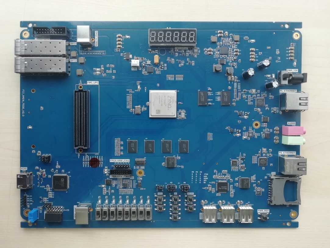
PE7030 Board Full View
1.Introduction
This development board uses Xilinx’s zynq7000 series chip, model XC7Z030-2FFG676I, 676-pin FPGA package. This chip can be divided into a PS (Processor System) part and a PL (Programmable Logic) part. On the PE7030 development board, the PS and PL sections of the XC7Z030 are both equipped with a wealth of external interfaces and devices for convenience use and functional verification.
In addition, as always, the USB Cable downloader circuit is integrated on the development board. Users only need to use a USB cable to download and debug the development board.
Hardware resources:
-
-
- Two DDR3 (PL end) and four DDR3 (PS end), the model is MT41J256M16HA-125.
- Onboard three oscillators are 200MHz oscillator, 156.25MHz programmable oscillator (si570), and 33.3333MHz oscillator, providing a stable clock source for the development board
- 6-digit common anode segment display, through dynamic scanning to achieve data display;
- One channel HDMI interface, able to display colorful pictures or camera video;
- One EEPROM chip with I2C interface, model M24C08;
- Two adaptive 10M/100M/Gigabit Ethernet interfaces, one for PS and one for PL;
- 8 independent buttons, 7 programmable buttons, 1 reset button;
- An adjustable resistor can be used to simulate voltage changes;
- 8-bit DIP switch
- 8-bit LED
- One 12-pin GPIO connector that complies with the PMOD interface standard;
- One 32M serial flash chip;
- Three JTAG interfaces, two for FPGA and ARM debug interfaces, and one for JTAG debug interface for RISC-V CPU. Built-in RISC-V CPU software debugger, no external RISC-V JTAG emulator required;
- One UART asynchronous serial interface;
- Audio input interface (green), audio output interface (red);
- 4 USB interfaces, 1 for the mouse and keyboard interface, 2 for the universal serial interface;
- 1 USB (USB-B interface) to UART interface for serial communication;
- A pair of 10 Gigabit fiber interfaces;
- One SD card holder for storing operating system images and file systems;
- 1 LPC interface;
-
2.Basic Features of PE7030
The schematics quoted in this article are intended to highlight the key points, and the circuits that are not related to the theme (such as protection circuits or filter circuits) will be neglected. Please pay attention to that. For the source material, please refer to the attached schematic.
As mentioned above, this development board FPGA model is XC7Z030-2FFG676I, which is Xilinx’s high-performance FPGA.
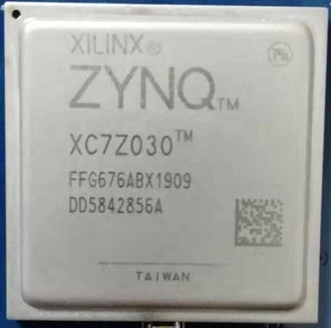
Figure 2.1 FPGA Physical Picture
Chip resources:
| Resource | Device |
| XC7Z030-2FFG676I | |
| Logic Cells | 125K |
| Look-Up Tables | 78,600 |
| Flip-Flops | 157,200 |
| Block RAM | 9.3Mb |
| DSP Slices | 400 |
| Peak DSP Performance | 593GMACs |
| PCI Express | Gen2 x4 |
| Pin Count | 676 |
Figure 2.2 Chip Resources
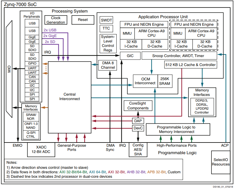
Figure 2. 3 Block Diagram of ZYNQ Chip
The main parameters of the PS system part are as follows:
– ARM dual-core CortexA9 based application processor, ARM-v7 architecture up to 1GHz
– 32KB level 1 instruction and data cache per CPU, two CPU share 512KB level 2 cache
– On-chip boot ROM and 256KB on-chip RAM
– External storage interface, support 16/32-bit DDR2, DDR3 interface
– Two Gigabit network interface cards support: divergent-aggregate DMA, GMII, RGMII, SGMII interface
– Two USB2.0 OTG interfaces, each supporting up to 12 nodes
– Two CAN2.0B bus interfaces
– Two SD card, SDIO, MMC compatible controllers
– Two SPIs, two UARTs, and two I2C interfaces
– 4 groups of 32-bit GPIO, 54 (32+22) bits as PS system I/O, 64 bits connected to PL
– High bandwidth connection within PS and from PS to PL
The chip is in a BGA package with 676 pins and a 1.0mm pin pitch. For the BGA packaged chip, the pin name is composed of “letter + number”, such as C8, E3, etc. The form of “letter + number” on the schematics represents the pins of the BGA.
The development board uses 12V DC power supply. (please use the power supply that comes with the development board, do not use other specifications of the power supply to avoid damage to the development board) Its power supply interface is as follows:
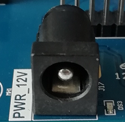
Figure 2. 3 Power Supply Interface Physical Picture
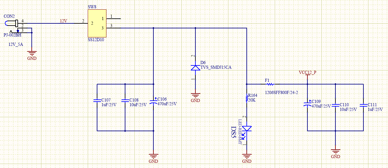
Figure 2. 4 Schematics of Power Supply
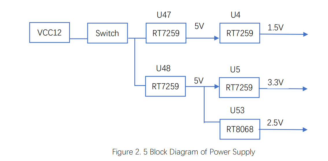
Figure 2. 5 Block Diagram of Power Supply
The development board inputs a 12V DC power supply and converts it into a 5V power supply through two RT7259s. After U4, U5, U53, 5V converts to 1.5V, 3.3V, 2.5V, and then converted to other required 1.0V, 1.8V, etc. through other circuits (for details, please refer to the schematic).
Onboard three oscillators, one piece is 200MHz, and one default is 156.25MHz programmable oscillator (si570). The other piece is the 33.3333MHz oscillator used on the PS side. The schematic is as follows:
Figure 3. 1 Schematics of Oscillator
Figure 3. 2 Schematics of Programmable Oscillator
Figure 3. 3 Schematics of 33.3333 MHz Oscillator
Physical picture:
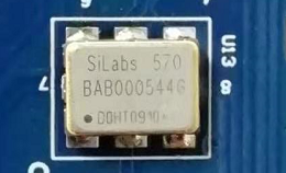
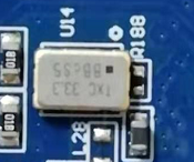
Figure 3. 4 Physical Picture of Oscillators
Pin assignment:
| Signal Name | FPGA Pin |
| CLK_200M_P | AC13 |
| CLK_200M_N | AD13 |
| USRCLK_P | AD20 |
| USRCLK_N | AD21 |
| PS_CLK | B24 |
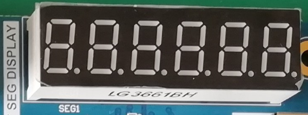
Figure 4. 1 Segment Display Decoders
One type of segment display is a semiconductor light-emitting device. The segment display can be divided into a seven-segment display decoder and an eight-segment display decoder. The difference is that the eight-segment display decoder has one more unit for displaying the decimal point, the basic unit is a light-emitting diode. The segment structure of the decoder is shown below:
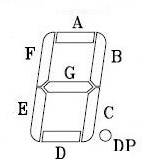
Figure 4.2 Segment Display Decoder Structure
Common anode decoders are used here. That is, the anodes of the LEDs are connected.
Figure 4.3 Schematics of Common Anode Decoders
To illuminate a segment of an 8-segment display decoder, the level of the corresponding pin needs to be pulled low; when the pin is set high, the corresponding segment will not light. This development board uses a 6-in-one eight-segment decoder. The schematics is shown below:
Figure 4.4 Schematic of Display Decoders
The six-in-one display decoder is a dynamic display. Due to the persistence of human vision and the afterglow effect of the LED, although the decoders are not lit at the same time, if the scanning speed is fast enough, the impression of human eyes is a group of stable display data, no flickering can be noticed. The same segments of the six-in-one decoders are connected, a total of eight pins, and with six control signal pins, a total of 14 pins, as shown in Figure 4.4. Among them SEG_PA, SEG_PB, SEG_PC, SEG_PD, SEG_PE, SEG_PF, SEG_PG, SEG_DP correspond to the A, B, C, D, E, F, G, DP of decoder; SEG_3V3_D [0..5] are six control pins of the decoders, which are also active low. When the control pin is low, the corresponding decoder is powered, so that the LED can be lit.
Pin assignments of display decoders
| Signal Name | FPGA Pin | Description |
| SEG PA | J10 | Segment A |
| SEG PB | J9 | Segment B |
| SEG PC | A7 | Segment C |
| SEG PD | B7 | Segment D |
| SEG PE | A8 | Segment E |
| SEG PF | A9 | Segment F |
| SEG PG | A10 | Segment G |
| SEG DP | B10 | Segment DP |
| SEG_D0_3V3 | C1 | Decoder 1(from right) |
| SEG_D1_3V3 | E3 | Decoder 2(from right) |
| SEG_D2_3V3 | F7 | Decoder 3(from right) |
| SEG_D3_3V3 | D6 | Decoder 4(from right) |
| SEG_D4_3V3 | H11 | Decoder 5(from right) |
| SEG_D5_3V3 | J11 | Decoder 6(from right) |
Image display processing has always been the focus of FPGA research. At present, the image display mode is also constantly developing. The image display interface is also gradually transitioning from the old VGA interface to the new DVI or HDMI interface. HDMI is the abbreviation of High Definition Multimedia Interface. It is a digital video/audio interface technology, which is a dedicated digital interface for image transmission. It can transmit audio and video signals at the same time.
The ADV7511 is a chip that converts FPGA digital signal to HDMI signal. For details, see the related chip manual. Among them, ADV7511_Programming_Guide and ADV7511_Hardware_Users_Guide are the most important. The registers of ADV7511 can be configured by viewing this document.
The chip communication address is selected by the PD pin, which can be 0x72 or 0x7A. The PD pin of this development board is grounded, so the communication address is 0x72.
Figure 5.1 HDMI Interface and ADV7511 Chip
HDMI pin assignment
| Signal Name | Pin Name | FPGA Pin |
| HDMI_INT | INT | W20 |
| HDMI_VSYNC | VSYNC | AE18 |
| HDMI_HSYNC | HSYNC | AA22 |
| HDMI_CLK | CLK | AD19 |
| HDMI_D23 | D35 | AB22 |
| HDMI_D22 | D34 | W19 |
| HDMI_D21 | D33 | AA24 |
| HDMI_D20 | D32 | AB20 |
| HDMI_D19 | D31 | AB21 |
| HDMI_D18 | D30 | AA19 |
| HDMI_D17 | D29 | AB24 |
| HDMI_D16 | D28 | AB19 |
| HDMI_D15 | D23 | AF25 |
| HDMI_D14 | D22 | AC19 |
| HDMI_D13 | D21 | AA23 |
| HDMI_D12 | D20 | AE20 |
| HDMI_D11 | D19 | AD23 |
| HDMI_D10 | D18 | AF20 |
| HDMI_D9 | D17 | AD26 |
| HDMI_D8 | D16 | AF24 |
| HDMI_D7 | D11 | AF19 |
| HDMI_D6 | D10 | AD25 |
| HDMI_D5 | D9 | AC22 |
| HDMI_D4 | D8 | AE23 |
| HDMI_D3 | D7 | AC21 |
| HDMI_D2 | D6 | AE26 |
| HDMI_D1 | D5 | AC18 |
| HDMI_D0 | D4 | AD18 |
| HDMI_DE | DE | AE25 |
| HDMI_I2S3 | SPDIF | AE21 |
| HDMI_MCLK | MCLK | Y20 |
| HDMI_I2S0 | I2S0 | AF23 |
| HDMI_I2S1 | I2S1 | AF22 |
| HDMI_I2S2 | I2S2 | AF18 |
| HDMI_I2S3 | I2S3 | AE21 |
| HDMI_SCLK | SCLK | W18 |
| HDMI_LRCLK | LRCLK | Y18 |
EEPROM is generally used in the instrumentation design. It is often used as a storage for some parameters. Data is not lost when power is off, and it is easy to operate. It is an ideal storage device.
The development board contains an EEPROM, model M24C08, with a capacity of 1k byte (1024*8bit), which communicates over the IIC bus.
IIC (Inter-Integrated Circuit) literally means between integrated circuits, which is the IIC Bus abbreviation. It is a serial communication bus, using multi-master-slave architecture, by Philips in the 1980s, developed to allow motherboards, embedded systems, or mobile phones to connect to low-speed peripherals. Also written as “I2C”, “I2C”, the correct reading is “I-squared-C”.
Figure 6.1 Schematics of EEPROM
The address lines A2, A1, and A0 of the chip are all connected to GND, so the communication address of the chip is 7’B1010000 (the first four addresses of the chip are fixed 1010).
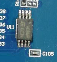
Figure 6.2 Physical Picture of EEPROM
This chip is connected to the I2C main bus via the PCA9548 and then to the FPGA.
The PCA9548 is an I2C bus expansion device from NXP, which can expand one I2C bus to eight. After the internal control register is configured accordingly, one or more downstream I2C can be selected for connection to the upstream I2C bus at the same time. The device can be restored to its default state by an external hardware reset—disconnecting the upstream and downstream buses to improve system reliability. Each I2C interface and interrupt input and output are open-drain, and all I/O ports can withstand an input voltage of 5V. The design schematic is as follows:
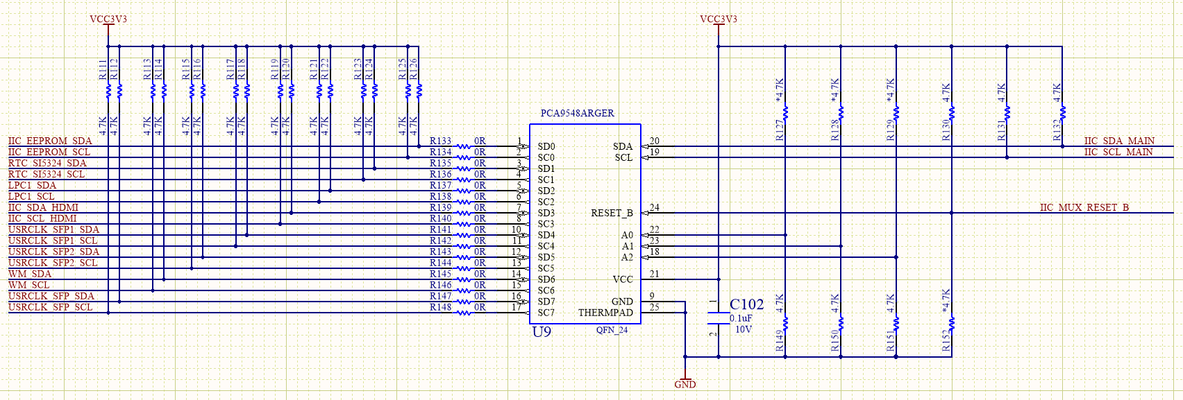
Figure 6. 3 PCA9548 I2C Bus Expansion
EEPROM pin assignment
| M24C08 Pin | PCA9548 Pin | FPGA Pin |
| SDA | 1 | W17 |
| SCL | 2 | W14 |
Ethernet is currently the most commonly used data communication method. Ethernet is getting faster and faster from the initial 10Mb/s to the later 100Mb/s, and to 1000Mb/s now.
PE7030 is equipped with an 88E1512 Gigabit Ethernet chip. The 88E1512 is a highly integrated network receiving PHY chip from Marvell. It is compliant with 10Base-T, 100Base-TX and 1000Base-T IEEE802.3 standards. It can transmit network data via CAT 5 UTP cable and CAT 3 UTP cable. It belongs to the physical layer in network communication and is used for data communication between MAC and PHY. Mainly used in network interface adapters, network hubs, gateways and some embedded devices.
The main features of the 88E1512 include:
1、Meets 1000Base-T IEEE802.3ab standard
2、Compliant with 100Base-TX IEEE802.3u standard
3、Compliant with 10Base-T IEEE802.3 standard
4、Support IEEE 802.3 RGMII interface
5、Support IEEE 802.3 GMII, MII interface
6、Support for Wake-on-LAN
7、Support for interrupt function
8、Support crossover detection and auto-correction
9、Support half-duplex, full-duplex operation
10、1000 MHz communication CAT 5 network cable can reach 100m
11、RGMII interface supports 3.3V, 2.5V, 1.8V, 1.5V signals
12、LED indications for three network states are available
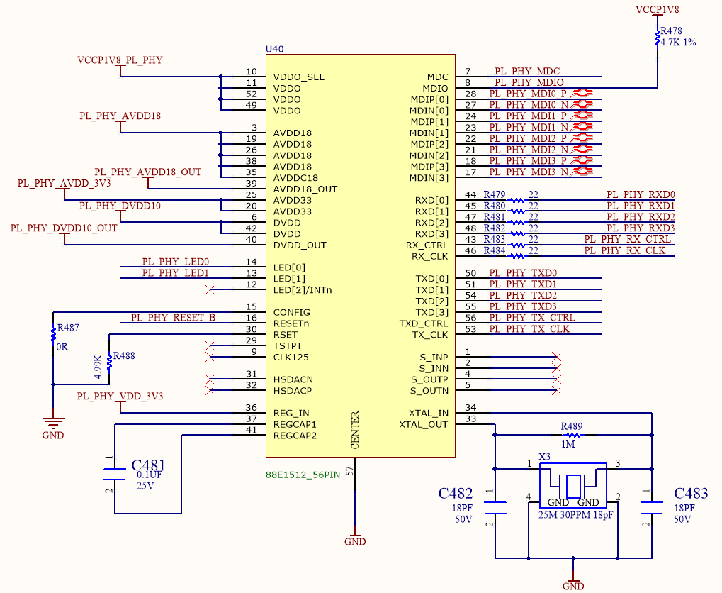
Figure 7.1 Schematics of Gigabit Ethernet Chip
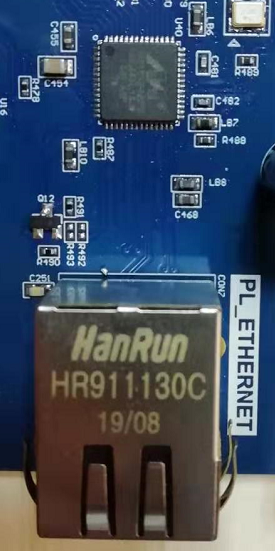
Figure 7.2 Gigabit Ethernet Physical Picture
Gigabit ethernet pin assignment
| 88E1512 Pin | Signal Name | FPGA Pin |
| MDC | PL_PHY_MDC | K8 |
| MDIO | PL_PHY_MDIO | K7 |
| RXD [0] | PL_PHY_RXD0 | K3 |
| RXD [1] | PL_PHY_RXD1 | K1 |
| RXD [2] | PL_PHY_RXD2 | H2 |
| RXD [3] | PL_PHY_RXD3 | G1 |
| RX_CTRL | PL_PHY_RX_CTRL | L3 |
| RX_CLK | PL_PHY_RX_CLK | J4 |
| TXD [0] | PL_PHY_TXD0 | M2 |
| TXD [1] | PL_PHY_TXD1 | L2 |
| TXD [2] | PL_PHY_TXD2 | L4 |
| TXD [3] | PL_PHY_TXD3 | L5 |
| TXD_CTRL | PL_PHY_TX_CTRL | K5 |
| TX_CLK | PL_PHY_TX_CLK | N3 |
The on-board button is a common push button, which is valid when pressed, and automatically pops up when released. A total of eight, respectively PB0 (MENU) PB1 (UP), PB2 (RETURN), PB3 (LEFT), PB4 (OK), PB5 (RIGHT), PB6 (DOWN) and a hardware reset button RESET. The default is low and presses high. The schematic diagram is shown in Figure 8. 1.
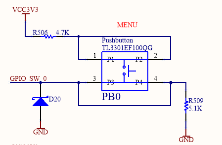
Figure 8.1 Schematics of Push Buttons (MENU)
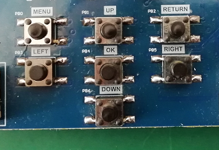
Figure 8.2 Push Button Physical Picture
Push button pin assignment
| Signal Name | FPGA Pin |
| MENU | L19 |
| UP | G4 |
| RETURN | F4 |
| LEFT | D4 |
| OK | D3 |
| RIGHT | F2 |
| DOWN | G2 |
A potentiometer is mounted on the board, and the resistance range is 0~1k ohms. The adjustable varistor is connected to the ADC part of the PS terminal and can be read its value directly. It is mainly used to learn the ADC function of SoC. The schematic is as follows:
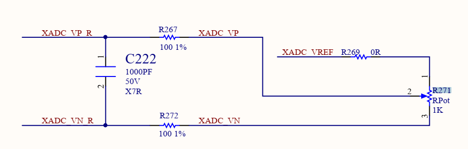
Figure 9. 1 Schematics of Potentiometer
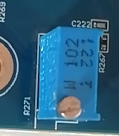
Figure 9. 2 Physical Picture of Potentiometer
Pin assignment:
| Potentiometer Pin | Network Name | ARM Pin | ARM Signal Name |
| 1 | XADC_VREF | P14 | VREFP_0 |
| 2 | XADC_VP_R | N14 | VP_0 |
| 3 | XADC_VN_R | P13 | VN_0 |
The 8-bit DIP switch and 8 LEDs are onboard. When the DIP switch is turned on, the FPGA pin gets high. If the FPGA pin is low, the corresponding LED will be on. The schematic diagram is as follows:
Figure 10.1 Schematics of DIP Switches

Figure 10.2 DIP Switches and LEDs Physical Picture
DIP switches and LED pin assignment
| Signal Name | FPGA Pin |
| SW0, LED0 | A17 |
| SW1, LED1 | E8 |
| SW2, LED2 | C6 |
| SW3, LED3 | B9 |
| SW4, LED4 | B6 |
| SW5, LED5 | H6 |
| SW6, LED6 | H7 |
| SW7, LED7 | G9 |
11)FMC-LPC High-speed Interface
The onboard FMC-LPC port is an inter-board high-speed connector that conforms to the VITA57 standard, the ASP series, has 160 contacts on the socket. The spacing between the socket contacts is 1.27mm, for a total of 4 rows of pins.
Figure 11. 1 FMC-LPC Physical Picture
FMC-LPC pin assignment:
| LPC Signal Name | Network Name | FPGA Pin |
| C2 (DP0_C2M_P) | FMC_MGT_RX_P | AB4 |
| C3 (DP0_C2M_N) | FMC_MGT_RX_N | AB3 |
| C6 (DP0_M2C_P) | FMC_MGT_TX_P | AA2 |
| C7 (DP0_M2C_N) | FMC_MGT_TX_N | AA1 |
| C10 (LA06_P) | NetLPC1_C10 | AB15 |
| C11 (LA06_N) | NetLPC1_C11 | AB14 |
| C14 (LA10_P) | LPC1_TX_D3_P | AF15 |
| C15 (LA10_N) | LPC1_TX_D3_N | AF14 |
| C18 (LA14_P) | LPC1_TX_D4_P | AD16 |
| C19 (LA14_N) | LPC1_TX_D4_N | AD15 |
| C26 (LA27_P) | LPC1_SPI_DI | AA12 |
| C27 (LA27_N) | LPC1_SPI_DO | Y13 |
| D8 (LA01_P_CC) | NetLPC1_D8 | AB17 |
| D9 (LA01_N_CC) | NetLPC1_D9 | AB16 |
| D11 (LA05_P) | NetLPC1_D11 | W16 |
| D12 (LA05_N) | NetLPC1_D12 | W15 |
| D14 (LA09_P) | LPC1_TX_FRAME_P | AE13 |
| D15 (LA09_N) | LPC1_TX_FRAME_N | AF13 |
| D17 (LA13_P) | LPC1_TX_D2_P | Y17 |
| D18 (LA13_N) | LPC1_TX_D2_N | AA17 |
| D23 (LA23_P) | LPC1_CTRL_OUT6 | J6 |
| D24 (LA23_N) | LPC1_CTRL_OUT7 | N7 |
| D26 (LA26_P) | LPC1_SPI_ENB | AA133 |
| D27 (LA26_N) | LPC1_SPI_CLK | W13 |
| G2 (CLK1_M2C_P) | FMC_MGT_CLK_P | U6 |
| G3 (CLK1_M2C_N) | FMC_MGT_CLK_N | U5 |
| G6 (LA00_P_CC) | LPC1_DATA_CLK_P | AC14 |
| G7 (LA00_N_CC) | LPC1_DATA_CLK_N | AD1 |
| G9 (LA03_P) | NetLPC1_G9 | AE17 |
| G10 (LA03_N) | NetLPC1_G10 | AF17 |
| G12 (LA08_P) | LPC1_FB_CLK_P | AE12 |
| G13 (LA08_N) | LPC1_FB_CLK_N | AF12 |
| G15 (LA12_P) | LPC1_TX_D1_P | AE16 |
| G16 (LA12_N) | LPC1_TX_D1_N | AE15 |
| G18 (LA16_P) | LPC1_ENABLE | AB10 |
| G19 (LA16_N) | LPC1_TXNRX | Y11 |
| G21 (LA20_P) | LPC1_CTRL_OUT0 | AB11 |
| G22 (LA20_N) | LPC1_CTRL_OUT1 | Y12 |
| G24 (LA22_P) | LPC1_CTRL_OUT4 | N1 |
| G25 (LA22_N) | LPC1_CTRL_OUT5 | M1 |
| G27 (LA25_P) | NetLPC1_G27 | N4 |
| G28 (LA25_N) | NetLPC1_G28 | M4 |
| H4 (CLK0_M2C_P) | LPC1_CLK_OUT | AD11 |
| H7 (LA02_P) | NetLPC1_H7 | AC17 |
| H8 (LA02_N) | NetLPC1_H8 | AC16 |
| H10 (LA04_P) | NetLPC1_H10 | AA15 |
| H11 (LA04_N) | NetLPC1_H11 | AA1 |
| H13 (LA07_P) | NetLPC1_H13 | Y16 |
| H14 (LA07_N) | NetLPC1_H14 | Y15 |
| H16 (LA11_P) | LPC1_TX_D0_P | AE11 |
| H17 (LA11_N) | LPC1_TX_D0_N | AF10 |
| H19 (LA15_P) | LPC1_TX_D5_P | AE10 |
| H20 (LA15_N) | LPC1_TX_D5_N | AD10 |
| H22 (LA19_P) | LPC1_EN_AGC | AC11 |
| H23 (LA19_N) | NetLPC1_H23 | AC12 |
| H25 (LA21_P) | LPC1_CTRL_OUT2 | AA10 |
| H26 (LA21_N) | LPC1_CTRL_OUT3 | AB12 |
| H28 (LA24_P) | NetLPC1_H28 | H3 |
| H29 (LA24_N) | NetLPC1_H29 | K2 |
| H31 (LA28_P) | LPC1_RESETB | Y10 |
The S25FL128SAGMFIR01 is a serial FLASH chip with a capacity of 128Mbit, which is more than enough for storing programs in the FPGA. Figure 12.1 shows the S25FL128SAGMFIR01 in the schematics.
Figure 12.1 Schematics of FLASH
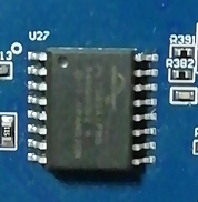
Figure 12.2 FLASH Physical Picture
Pin assignment:
| FLASH Pin | Signal Name | FPGA Pin |
| HOLD_B_I03 | QSPI1_IO3 | N6 |
| CS_B | QSPI1_SC_B | N8 |
| SO_IO1 | QSPI1_IO1 | M7 |
| SCK | QSPI1_CLK | D1 |
| SI_IO0 | QSPI1_IO0 | J3 |
| WP_B_IO2 | QSPI1_IO2 | K6 |
13)GPIO (PMOD) Expansion Interface
The development board has one GPIO interface, including FPGA resource with 6 standard I/O pins, 2 GND signals, and 2 adjustable power supply (3.3V, 5V) pins. The schematic is as follows:
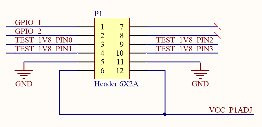
Figure 13.1 Schematics of GPIO
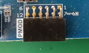
Figure 13.2 GPIO Physical Picture
GPIO pin assignment
| Signal Name | FPGA Pin | Description |
| P1-1 | E1 | Standard IO |
| P1-2 | F3 | Standard IO |
| P1-3 | E2 | Standard IO |
| P1-4 | J1 | Standard IO |
| P1-5 | GND | |
| P1-6 | VCC | |
| P1-7 | NULL | |
| P1-8 | NULL | |
| P1-9 | H11 | Standard IO |
| P1-10 | H4 | Standard IO |
| P1-11 | GND | |
| P1-12 | VCC |
14)FPGA Downloader and RISC-V Downloader
The development board provides two JTAG interfaces for FPGA download, which are J10 (2.54mm pitch pin) and J8 (2.00mm box header). The JTAG schematics is shown in Figure 14. 1:
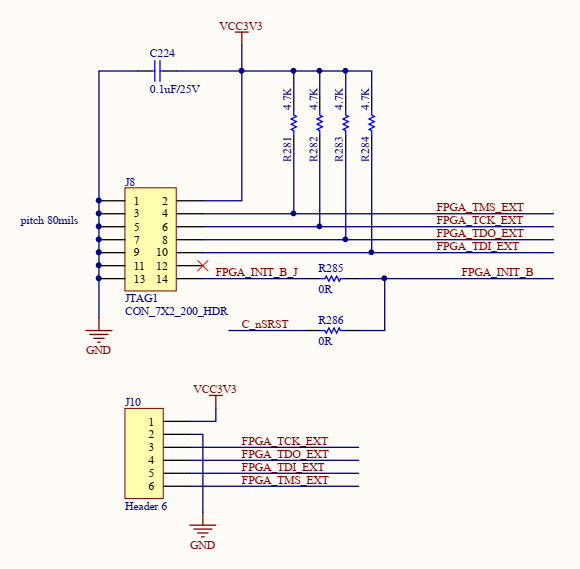
Figure 14.1 Schematics of JTAG Interface
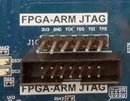
Figure 14.2 JTAG Interface Physical Picture
There are also two RISC-V download interfaces, as shown in the following figure. The program can be downloaded for the RISC-V CPU. The physical and pin assignments are as follows:
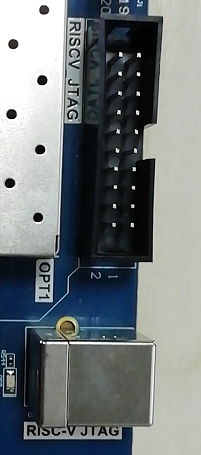
Figure 14. 3 RISC-V Download Interface Physical Picture
RISC-V download interface pin assignment
| Network Name | J1 Pin | FPGA Pin |
| RISCV_n | 3 | V19 |
| RISCV_TTDI | 5 | AA25 |
| RISCV_TTMS | 7 | AB26 |
| RISCV_TTCK | 9 | AC23 |
| RISCV_TRTCK | 11 | AC23 |
| RISCV_TTDO | 13 | AB25 |
| RISCV_TSRST_n | 15 | AD24 |
Two USB-B interfaces and two FT2232 chips are onboard for FPGA or CPU program downloads, as well as serial data communication.
Refer the design drawings for the schematics diagram. The physical picture is shown below:
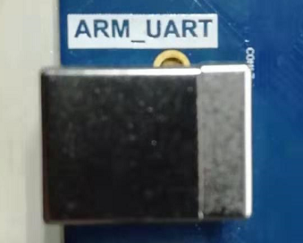
Figure 15. 2 USB-B Interface
UART pin assignment
| Signal Name | FPGA Pin |
| (RISC-V JTAG) TX | AC26 |
| (RISC-V JTAG) RX | AE22 |
| (ARM-UART) TX | B22 |
| (ARM-UART) RX | B20 |
DDR3, or full name DDR3 SDRAM (Synchronous Dynamic Random-Access Memory) is a memory specification. Compared to SRAM, data stored in DRAM needs to be updated periodically. The development board has six DDR3s, of which 4 are on PS end, the capacity is 256M * 8bit, and 2 are on the PL end, and the capacity is 256M*16bit. Some of the schematics are as follows (see the design drawings for complete information):
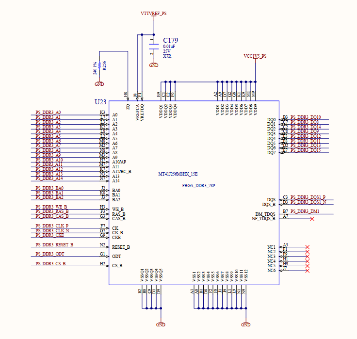
Figure 16. 1 Schematics of DDR3
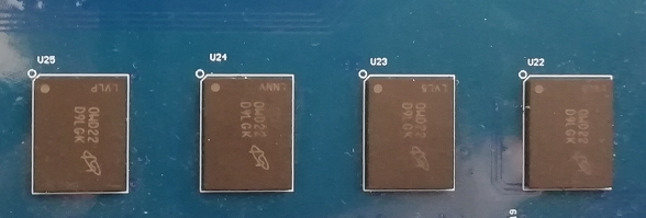
Figure 16. 2 Physical Picture of DDR3
Pin assignment:
| DDR3 Pin (Signal Name) | Network Name | FPGA Pin |
| U38-A2 (PL_DDR_DQ13) | DQ13 | G16 |
| U38-A3 (PL_DDR_DQ15) | DQ15 | G14 |
| U38-A7 (PL_DDR_DQ12) | DQ12 | H13 |
| U38-B7 (PL_DDR_DQS1_N) | UDQS# | J15 |
| U38-B8 (PL_DDR_DQ14) | DQ14 | H12 |
| U38-C2 (PL_DDR_DQ11) | DQ11 | J14 |
| U38-C3 (PL_DDR_DQ9) | DQ9 | F14 |
| U38-C7 (PL_DDR_DQS1_P) | UDQS | K15 |
| U38-C8 (PL_DDR_DQ10) | DQ10 | J13 |
| U38-D3 (PL_DDR_DM1) | UDM | G15 |
| U38-D7 (PL_DDR_DQ8) | DQ8 | K13 |
| U38-E3 (PL_DDR_DQ0) | DQ0 | E12 |
| U38-E7 (PL_DDR_DM0) | LDM | E11 |
| U38-F2 (PL_DDR_DQ2) | DQ2 | F13 |
| U38-F3 (PL_DDR_DQS0_P) | LDQS | G10 |
| U38-F7 (PL_DDR_DQ1) | DQ1 | D10 |
| U38-F8 (PL_DDR_DQ3) | DQ3 | E10 |
| U38-G2 (PL_DDR_DQ6) | DQ6 | D11 |
| U38-G3 (PL_DDR_DQS0_N) | LDQS# | F10 |
| U38-H1 (VTTVREF_PL) | VREFDQ | C8 |
| U38-H3 (PL_DDR_DQ4) | DQ4 | F12 |
| U38-H7 (PL_DDR_DQ7) | DQ7 | G11 |
| U38-H8 (PL_DDR_DQ5) | DQ5 | G12 |
| U38-J3 (PL_DDR_RAS_N) | RAS# | C9 |
| U38-J7 (PL_DDR_CK_P) | CK | C8 |
| U38-K1 (PL_DDR_DOT0) | ODT | A4 |
| U38-K3 (PL_DDR_CAS_N) | CAS# | A2 |
| U38-K7 (PL_DDR_CK_N) | CK# | C7 |
| U38-K9 (PL_DDR_CKE_0) | CKE | D9 |
| U38-L2 (PL_DDR_CS_N) | CS# | A5 |
| U38-L3 (PL_DDR_WE_N) | WE# | D8 |
| U38-L7 (PL_DDR_A10) | A10/AP | A3 |
| U38-M2 (PL_DDR_BA0) | BA0 | C4 |
| U38-M3 (PL_DDR_BA2) | BA2 | B1 |
| U38-M7 (PL_DDR_A15) | NC | B5 |
| U38-M8 (VTTVREF_PL) | VREFCA | C8 |
| U38-N2 (PL_DDR_A3) | A3 | B4 |
| U38-N3 (PL_DDR_A0) | A0 | E7 |
| U38-N7 (PL_DDR_A12) | A12/BC# | C2 |
| U38-N8 (PL_DDR_BA1) | BA1 | C3 |
| U38-P2 (PL_DDR_A5) | A5 | G7 |
| U38-P3 (PL_DDR_A2) | A2 | D5 |
| U38-P7 (PL_DDR_A1) | A1 | E6 |
| U38-P8 (PL_DDR_A4) | A4 | B2 |
| U38-R2 (PL_DDR_A7) | A7 | F9 |
| U38-R3 (PL_DDR_A9) | A9 | G5 |
| U38-R7 (PL_DDR_A11) | A11 | E5 |
| U38-R8 (PL_DDR_A6) | A6 | F5 |
| U38-T2 (PL_DDR_RST_N) | RESET# | H14 |
| U38-T3 (PL_DDR_A13) | A13 | J8 |
| U38-T7 (PL_DDR_A14) | A14 | F8 |
| U38-T8 (PL_DDR_A8) | A8 | G6 |
| U39-A2 (PL_DDR_DQ13) | DQ13 | C14 |
| U39-A3 (PL_DDR_DQ15) | DQ15 | B14 |
| U39-A7 (PL_DDR_DQ12) | DQ12 | D13 |
| U39-B7 (PL_DDR_DQS1_N) | UDQS# | A14 |
| U39-B8 (PL_DDR_DQ14) | DQ14 | C12 |
| U39-C2 (PL_DDR_DQ11) | DQ11 | C11 |
| U39-C3 (PL_DDR_DQ9) | DQ9 | A13 |
| U39-C7 (PL_DDR_DQS1_P) | UDQS | A15 |
| U39-C8 (PL_DDR_DQ10) | DQ10 | B12 |
| U39-D3 (PL_DDR_DM1) | UDM | B11 |
| U39-D7 (PL_DDR_DQ8) | DQ8 | A12 |
| U39-E3 (PL_DDR_DQ0) | DQ0 | B17 |
| U39-E7 (PL_DDR_DM0) | LDM | B16 |
| U39-F2 (PL_DDR_DQ2) | DQ2 | D16 |
| U39-F3 (PL_DDR_DQS0_P) | LDQS | C17 |
| U39-F7 (PL_DDR_DQ1) | DQ1 | D15 |
| U39-F8 (PL_DDR_DQ3) | DQ3 | D14 |
| U39-G2 (PL_DDR_DQ6) | DQ6 | E16 |
| U39-G3 (PL_DDR_DQS0_N) | LDQS# | C16 |
| U39-H1 (VTTVREF_PL) | VREFDQ | C8 |
| U39-H3 (PL_DDR_DQ4) | DQ4 | F15 |
| U39-H7 (PL_DDR_DQ7) | DQ7 | B15 |
| U39-H8 (PL_DDR_DQ5) | DQ5 | E15 |
| U39-J3 (PL_DDR_RAS_N) | RAS# | C9 |
| U39-J7 (PL_DDR_CK_P) | CK | C8 |
| U39-K1 (PL_DDR_DOT0) | ODT | A4 |
| U39-K3 (PL_DDR_CAS_N) | CAS# | A2 |
| U39-K7 (PL_DDR_CK_N) | CK# | C7 |
| U39-K9 (PL_DDR_CKE_0) | CKE | D9 |
| U39-L2 (PL_DDR_CS_N) | CS# | A5 |
| U39-L3 (PL_DDR_WE_N) | WE# | D8 |
| U39-L7 (PL_DDR_A10) | A10/AP | A3 |
| U39-M2 (PL_DDR_BA0) | BA0 | C4 |
| U39-M3 (PL_DDR_BA2) | BA2 | B1 |
| U39-M7 (PL_DDR_A15) | NC | B5 |
| U39-M8 (VTTVREF_PL) | VREFCA | C8 |
| U39-N2 (PL_DDR_A3) | A3 | B4 |
| U39-N3 (PL_DDR_A0) | A0 | E7 |
| U39-N7 (PL_DDR_A12) | A12/BC# | C2 |
| U39-N8 (PL_DDR_BA1) | BA1 | C3 |
| U39-P2 (PL_DDR_A5) | A5 | G7 |
| U39-P3 (PL_DDR_A2) | A2 | D5 |
| U39-P7 (PL_DDR_A1) | A1 | E6 |
| U39-P8 (PL_DDR_A4) | A4 | B2 |
| U39-R2 (PL_DDR_A7) | A7 | F9 |
| U39-R3 (PL_DDR_A9) | A9 | G5 |
| U39-R7 (PL_DDR_A11) | A11 | E5 |
| U39-R8 (PL_DDR_A6) | A6 | F5 |
| U39-T2 (PL_DDR_RST_N) | RESET# | H14 |
| U39-T3 (PL_DDR_A13) | A13 | J8 |
| U39-T7 (PL_DDR_A14) | A14 | F8 |
| U39-T8 (PL_DDR_A8) | A8 | G6 |
| DDS3 Pin (Signal Name) | Network Name | PS Pin |
| U22-B3 (PS_DDR3_DQ3) | DQ0 | G26 |
| U22-B7 (PS_DDR3_DM0) | DM_TDQS | G24 |
| U22-C2 (PS_DDR3_DQ4) | DQ2 | H26 |
| U22-C3 (PS_DDR3_DQS0_P) | DQS | H24 |
| U22-C7 (PS_DDR3_DQ1) | DQ1 | F25 |
| U22-C8 (PS_DDR3_DQ6) | DQ3 | J24 |
| U22-D2 (PS_DDR3_DQ2) | DQ6 | J25 |
| U22-D3 (PS_DDR3_DQS0_N) | DQS_B | G25 |
| U22-E1 (VTTVREF_PS) | VREFDQ | M21 |
| U22-E3 (PS_DDR3_DQ0) | DQ4 | J26 |
| U22-E7 (PS_DDR3_DQ5) | DQ7 | H23 |
| U22-E8 (PS_DDR3_DQ7) | DQ5 | J23 |
| U22-F3 (PS_DDR3_RAS_B) | RAS_B | V23 |
| U22-F7 (PS_DDR3_CLK_P) | CK | R21 |
| U22-G1 (PS_DDR3_ODT) | ODT | Y22 |
| U22-G3 (PS_DDR3_CAS_B) | CAS_B | Y23 |
| U22-G7 (PS_DDR3_CLK_N) | CK_B | P21 |
| U22-G9 (PS_DDR3_CKE) | CKE | U21 |
| U22-H2 (PS_DDR3_CS_B) | CS_B | Y21 |
| U22-H3 (PS_DDR3_WE_B) | WE_B | V22 |
| U22-H7 (PS_DDR3_A10) | A10/AP | M22 |
| U22-J2 (PS_DDR3_BA0) | BA0 | U22 |
| U22-J3 (PS_DDR3_BA2) | BA2 | R22 |
| U22-J8 (VTTVREF_PS) | VREFCA | M21 |
| U22-K2 (PS_DDR3_A3) | A3 | L22 |
| U22-K3 (PS_DDR3_A0) | A0 | K22 |
| U22-K7 (PS_DDR3_A12) | A12/BC_B | P20 |
| U22-K8 (PS_DDR3_BA1) | BA1 | T22 |
| U22-L2 (PS_DDR3_A5) | A5 | N22 |
| U22-L3 (PS_DDR3_A2) | A2 | N21 |
| U22-L7 (PS_DDR3_A1) | A1 | K20 |
| U22-L8 (PS_DDR3_A4) | A4 | M20 |
| U22-M2 (PS_DDR3_A7) | A7 | J21 |
| U22-M3 (PS_DDR3_A9) | A9 | U20 |
| U22-M7 (PS_DDR3_A11) | A11 | H21 |
| U22-M8 (PS_DDR3_A6) | A6 | L20 |
| U22-N2 (PS_DDR3_RESET_B) | RESET_B | H22 |
| U22-N3 (PS_DDR3_A13) | A13 | J20 |
| U22-N7 (PS_DDR3_A14) | A14 | R20 |
| U22-N8 (PS_DDR3_A8) | A8 | T20 |
| U23-B3 (PS_DDR3_DQ3) | DQ0 | M26 |
| U23-B7 (PS_DDR3_DM0) | DM_TDQS | K25 |
| U23-C2 (PS_DDR3_DQ4) | DQ2 | M24 |
| U23-C3 (PS_DDR3_DQS0_P) | DQS | L24 |
| U23-C7 (PS_DDR3_DQ1) | DQ1 | K26 |
| U23-C8 (PS_DDR3_DQ6) | DQ3 | L23 |
| U23-D2 (PS_DDR3_DQ2) | DQ6 | N24 |
| U23-D3 (PS_DDR3_DQS0_N) | DQS_B | L25 |
| U23-E1 (VTTVREF_PS) | VREFDQ | M21 |
| U23-E3 (PS_DDR3_DQ0) | DQ4 | M25 |
| U23-E7 (PS_DDR3_DQ5) | DQ7 | N23 |
| U23-E8 (PS_DDR3_DQ7) | DQ5 | K23 |
| U23-F3 (PS_DDR3_RAS_B) | RAS_B | V23 |
| U23-F7 (PS_DDR3_CLK_P) | CK | R21 |
| U23-G1 (PS_DDR3_ODT) | ODT | Y22 |
| U23-G3 (PS_DDR3_CAS_B) | CAS_B | Y23 |
| U23-G7 (PS_DDR3_CLK_N) | CK_B | P21 |
| U23-G9 (PS_DDR3_CKE) | CKE | U21 |
| U23-H2 (PS_DDR3_CS_B) | CS_B | Y21 |
| U23-H3 (PS_DDR3_WE_B) | WE_B | V22 |
| U23-H7 (PS_DDR3_A10) | A10/AP | M22 |
| U23-J2 (PS_DDR3_BA0) | BA0 | U22 |
| U23-J3 (PS_DDR3_BA2) | BA2 | R22 |
| U23-J8 (VTTVREF_PS) | VREFCA | M21 |
| U23-K2 (PS_DDR3_A3) | A3 | L22 |
| U23-K3 (PS_DDR3_A0) | A0 | K22 |
| U23-K7 (PS_DDR3_A12) | A12/BC_B | P20 |
| U23-K8 (PS_DDR3_BA1) | BA1 | T22 |
| U23-L2 (PS_DDR3_A5) | A5 | N22 |
| U23-L3 (PS_DDR3_A2) | A2 | N21 |
| U23-L7 (PS_DDR3_A1) | A1 | K20 |
| U23-L8 (PS_DDR3_A4) | A4 | M20 |
| U23-M2 (PS_DDR3_A7) | A7 | J21 |
| U23-M3 (PS_DDR3_A9) | A9 | U20 |
| U23-M7 (PS_DDR3_A11) | A11 | H21 |
| U23-M8 (PS_DDR3_A6) | A6 | L20 |
| U23-N2 (PS_DDR3_RESET_B) | RESET_B | H22 |
| U23-N3 (PS_DDR3_A13) | A13 | J20 |
| U23-N7 (PS_DDR3_A14) | A14 | R20 |
| U23-N8 (PS_DDR3_A8) | A8 | T20 |
| U24-B3 (PS_DDR3_DQ3) | DQ0 | T25 |
| U24-B7 (PS_DDR3_DM0) | DM_TDQS | P26 |
| U24-C2 (PS_DDR3_DQ4) | DQ2 | T24 |
| U24-C3 (PS_DDR3_DQS0_P) | DQS | P25 |
| U24-C7 (PS_DDR3_DQ1) | DQ1 | P23 |
| U24-C8 (PS_DDR3_DQ6) | DQ3 | P24 |
| U24-D2 (PS_DDR3_DQ2) | DQ6 | T23 |
| U24-D3 (PS_DDR3_DQS0_N) | DQS_B | R25 |
| U24-E1 (VTTVREF_PS) | VREFDQ | M21 |
| U24-E3 (PS_DDR3_DQ0) | DQ4 | R26 |
| U24-E7 (PS_DDR3_DQ5) | DQ7 | R23 |
| U24-E8 (PS_DDR3_DQ7) | DQ5 | N26 |
| U24-F3 (PS_DDR3_RAS_B) | RAS_B | V23 |
| U24-F7 (PS_DDR3_CLK_P) | CK | R21 |
| U24-G1 (PS_DDR3_ODT) | ODT | Y22 |
| U24-G3 (PS_DDR3_CAS_B) | CAS_B | Y23 |
| U24-G7 (PS_DDR3_CLK_N) | CK_B | P21 |
| U24-G9 (PS_DDR3_CKE) | CKE | U21 |
| U24-H2 (PS_DDR3_CS_B) | CS_B | Y21 |
| U24-H3 (PS_DDR3_WE_B) | WE_B | V22 |
| U24-H7 (PS_DDR3_A10) | A10/AP | M22 |
| U24-J2 (PS_DDR3_BA0) | BA0 | U22 |
| U24-J3 (PS_DDR3_BA2) | BA2 | R22 |
| U24-J8 (VTTVREF_PS) | VREFCA | M21 |
| U24-K2 (PS_DDR3_A3) | A3 | L22 |
| U24-K3 (PS_DDR3_A0) | A0 | K22 |
| U24-K7 (PS_DDR3_A12) | A12/BC_B | P20 |
| U24-K8 (PS_DDR3_BA1) | BA1 | T22 |
| U24-L2 (PS_DDR3_A5) | A5 | N22 |
| U24-L3 (PS_DDR3_A2) | A2 | N21 |
| U24-L7 (PS_DDR3_A1) | A1 | K20 |
| U24-L8 (PS_DDR3_A4) | A4 | M20 |
| U24-M2 (PS_DDR3_A7) | A7 | J21 |
| U24-M3 (PS_DDR3_A9) | A9 | U20 |
| U24-M7 (PS_DDR3_A11) | A11 | H21 |
| U24-M8 (PS_DDR3_A6) | A6 | L20 |
| U24-N2 (PS_DDR3_RESET_B) | RESET_B | H22 |
| U24-N3 (PS_DDR3_A13) | A13 | J20 |
| U24-N7 (PS_DDR3_A14) | A14 | R20 |
| U24-N8 (PS_DDR3_A8) | A8 | T20 |
| U25-B3 (PS_DDR3_DQ3) | DQ0 | V24 |
| U25-B7 (PS_DDR3_DM0) | DM_TDQS | V26 |
| U25-C2 (PS_DDR3_DQ4) | DQ2 | W23 |
| U25-C3 (PS_DDR3_DQS0_P) | DQS | W24 |
| U25-C7 (PS_DDR3_DQ1) | DQ1 | U26 |
| U25-C8 (PS_DDR3_DQ6) | DQ3 | W26 |
| U25-D2 (PS_DDR3_DQ2) | DQ6 | Y25 |
| U25-D3 (PS_DDR3_DQS0_N) | DQS_B | W25 |
| U25-E1 (VTTVREF_PS) | VREFDQ | M21 |
| U25-E3 (PS_DDR3_DQ0) | DQ4 | Y26 |
| U25-E7 (PS_DDR3_DQ5) | DQ7 | U25 |
| U25-E8 (PS_DDR3_DQ7) | DQ5 | U24 |
| U25-F3 (PS_DDR3_RAS_B) | RAS_B | V23 |
| U25-F7 (PS_DDR3_CLK_P) | CK | R21 |
| U25-G1 (PS_DDR3_ODT) | ODT | Y22 |
| U25-G3 (PS_DDR3_CAS_B) | CAS_B | Y23 |
| U25-G7 (PS_DDR3_CLK_N) | CK_B | P21 |
| U25-G9 (PS_DDR3_CKE) | CKE | U21 |
| U25-H2 (PS_DDR3_CS_B) | CS_B | Y21 |
| U25-H3 (PS_DDR3_WE_B) | WE_B | V22 |
| U25-H7 (PS_DDR3_A10) | A10/AP | M22 |
| U25-J2 (PS_DDR3_BA0) | BA0 | U22 |
| U25-J3 (PS_DDR3_BA2) | BA2 | R22 |
| U25-J8 (VTTVREF_PS) | VREFCA | M21 |
| U25-K2 (PS_DDR3_A3) | A3 | L22 |
| U25-K3 (PS_DDR3_A0) | A0 | K22 |
| U25-K7 (PS_DDR3_A12) | A12/BC_B | P20 |
| U25-K8 (PS_DDR3_BA1) | BA1 | T22 |
| U25-L2 (PS_DDR3_A5) | A5 | N22 |
| U25-L3 (PS_DDR3_A2) | A2 | N21 |
| U25-L7 (PS_DDR3_A1) | A1 | K20 |
| U25-L8 (PS_DDR3_A4) | A4 | M20 |
| U25-M2 (PS_DDR3_A7) | A7 | J21 |
| U25-M3 (PS_DDR3_A9) | A9 | U20 |
| U25-M7 (PS_DDR3_A11) | A11 | H21 |
| U25-M8 (PS_DDR3_A6) | A6 | L20 |
| U25-N2 (PS_DDR3_RESET_B) | RESET_B | H22 |
| U25-N3 (PS_DDR3_A13) | A13 | J20 |
| U25-N7 (PS_DDR3_A14) | A14 | R20 |
| U25-N8 (PS_DDR3_A8) | A8 | T20 |
There is a piece WM8978 onboard, which is a stereo multimedia digital signal codec with speaker driver. The WM8978 is a low power, high quality stereo multimedia digital signal codec. It is mainly used in portable applications such as digital cameras and portable digital camcorders. It combines stereo differential microphone preamplifiers with speakers, headphones and differential, stereo line output drivers to reduce the external components necessary for the application, such as advanced on-chip digital signal processing function with separate microphone or headphone amplifiers, including a 5-band equalizer, a mixed signal Automatic Level Control for the microphone or line input through the ADC as well as a purely digital limiter function for record or playback. The WM8978 digital audio interface can operate as a master or a slave. An internal PLL can generate all required audio clocks for the CODEC from common reference clock frequencies. The chip’s communication address is fixed at 7’B0011010.
The schematic is as follows.
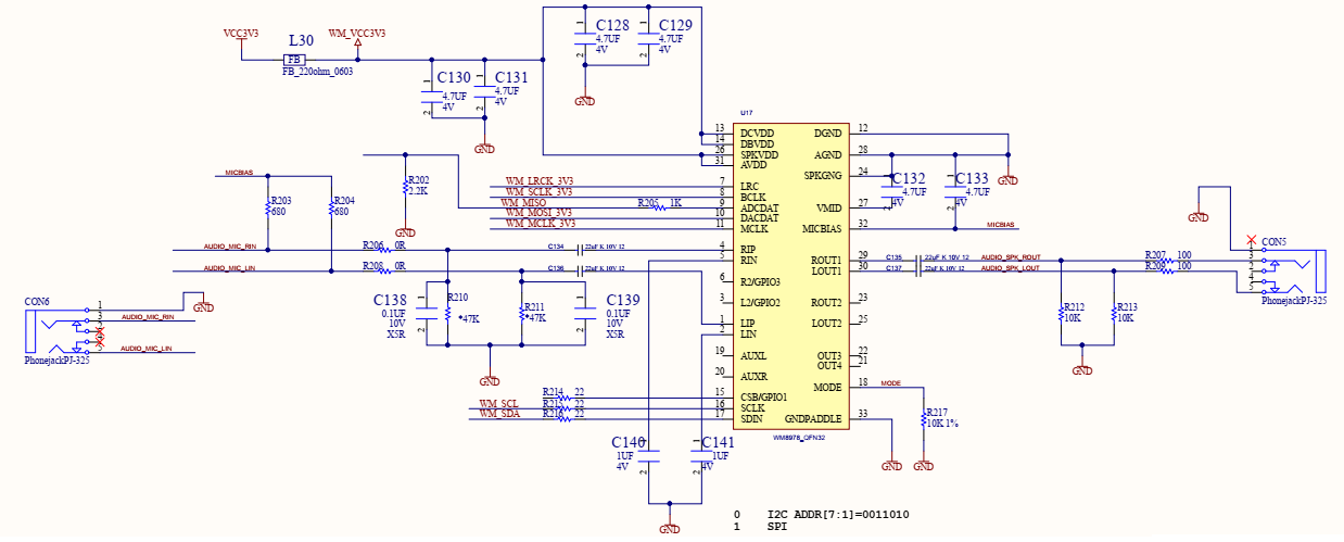
Figure 17.1 Schematics of Audio
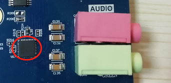
Figure 17.2 Audio Interface and Chip Physical Picture
Pin assignment:
| WM8978 Pin (Signal Name) | FPGA Pin |
| 7(LRC) | M8 |
| 8(BCLK) | L8 |
| 9(ADCDAT) | N2 |
| 10(DACDAT) | N2 |
| 11(MCLK) | L7 |
| 16(SCLK) | U9-SC6 |
| 17(SDIN) | U9-SD6 |
The TUSB4041I is a four-port USB 2.0 hub. The device provides USB high speed or full speed connectivity on the upstream port. The device also provides USB high speed, full speed or low speed connections on the downstream port. High speed, full speed, and low speed USB connections on the downstream port are enabled when the upstream port is connected to an electrical environment that only supports high speed, full speed, and low speed connections. When the upstream port is connected to an electrical environment that only supports full-speed or low-speed connections, the USB high-speed connection on the downstream port is disabled.
The TUSB4041I device provides pin-over configuration for select functions including battery charging support, as well as customizable PID, VID, custom port and physical layer configurations via the OTP ROM, I2C EEPROM, or through I2C and SM Bus slave interfaces. Custom string support is also available when using I2C EEPROM or I2C and SM Bus controlled interfaces.
The device is available in a 64-pin PAP package and the industrial version operates from -40°C to 85°C.
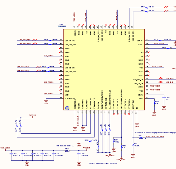
Figure 18. 1 Schematics of USB
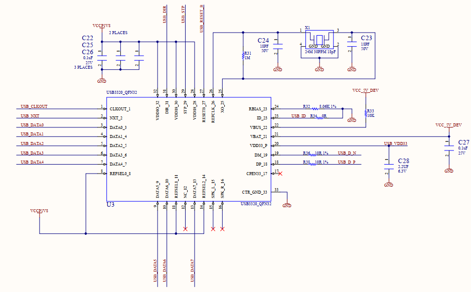
Figure 18. 2 Schematic USB Transceiver Section
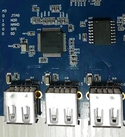
Figure 18. 3 USB Interface Physical Picture
Pin assignment:
| USB Pin (Signal Name) | FPGA Pin |
| U3-1(CLK_OUT) | K16 |
| U3-2(NXT) | E12 |
| U3-3(DATA0) | K17 |
| U3-4(DATA1) | E22 |
| U3-5(DATA2) | J16 |
| U3-6(DATA3) | D19 |
| U3-7(DATA4) | J18 |
| U3-9(DATA5) | D20 |
| U3-10(DATA6) | D21 |
| U3-13(DATA7) | C21 |
| U3-29(STP) | K19 |
| U3-31(DIR) | E20 |
The PE7030 development board includes an SD card interface to provide user access to the SD card memory, the BOOT program for storing the ZYNQ chip, the Linux operating system kernel, the file system, and other user data files. The SDIO signal is connected to the IO signal of the PS BANK501 of ZYNQ because the VCCMIO of the BANK is set to 1.8V, but the data voltage level of the SD card is 3.3V, which is connected by the TXS0102 and MAX13035E voltage level shifters. The schematics of the Zynq7000 PS and SD card connectors is shown in Figure 19. 1 to Figure 19. 3.
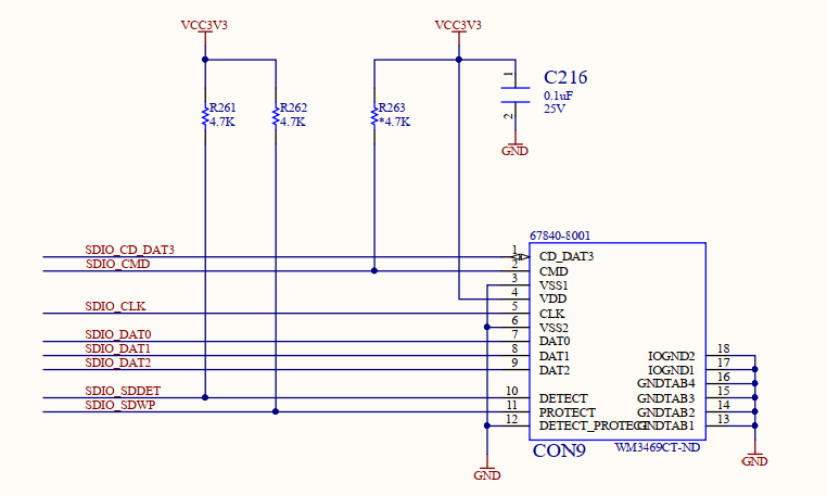
Figure 19. 1 Schematics of SD Card
Figure 19. 2 Schematics of the voltage level shifting chip MAX13035E
Figure 19. 3 Schematics of the voltage level shifting chip TXS0102
Figure 19. 4 SD Card Physical Picture
Pin assignment:
| Signal Name | ZYNQ Pin Name | ZYNQ Pin | Description |
| SDIO_CD_DAT3 | PS_MIO45 | C18 | SD Card Inserting Signal |
| SDIO_CMD | PS_MIO41 | C19 | SD Order Signal |
| SDIO_CLK | PS_MIO40 | C22 | SD Clock Signal |
| SDIO_DAT0 | PS_MIO42 | F17 | SD Data0 |
| SDIO_DAT1 | PS_MIO43 | D18 | SD Data1 |
| SDIO_DAT2 | PS_MIO44 | E18 | SD Data2 |
| SDIO_SDDET | PS_MIO48 | B21 | |
| SDIO_SDWP | PS_MIO49 | A18 |
Figure 20. 1 Physical Picture of Fiber Optic Interface
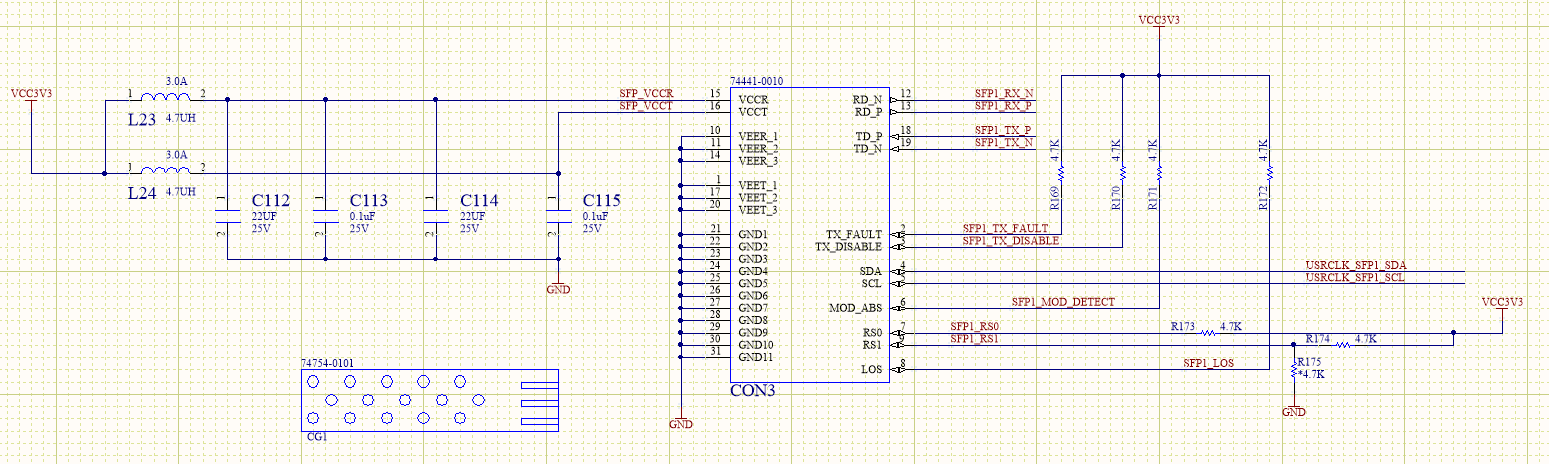
Figure 20. 2 Schematics of Fiber Optic Interface
Pin assignment:
| Pin (Signal Name) | FPGA Pin |
| Con3-12(SFP1-RX-N) | T3 |
| Con3-13(SFP1-RX-P) | T4 |
| Con3-18(SFP1-TX-P) | R2 |
| Con3-19(SFP1-TX-N) | R1 |
| Con4-12(SFP1-RX-N) | V4 |
| Con4-13(SFP1-RX-P) | V3 |
| Con4-18(SFP1-TX-P) | U2 |
| Con4-19(SFP1-TX-N) | U1 |
V1.1