Text Description automatically generated
FII-BD7100 FII-PE7030 PetaLinux SOC Tutor

How to Use RCP, SCP, and TFTP 6 With FII-PE7030, FII-BD7100 Development Board

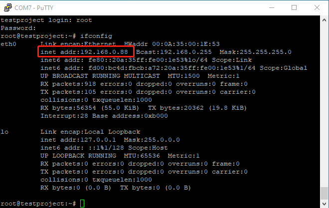
Table of Contents Copyright Notice 2 Section 1: Using RCP and SCP to Transfer Files 3 Section 2: Using TFTP 6 Copyright Notice: © 2020 Fraser Innovation Inc ALL RIGHTS RESERVED Without written permission of Fraser Innovation Inc, no unit or individual may extract or modify part of or all the contents of this manual. Offenders will be held liable for their legal responsibility. Thank you for purchasing the FPGA development board. Please read the manual carefully before using the product and make sure that you know how to use…

Read More
Text Description automatically generated
FII-BD7100 FII-PE7030 SOC Tutor

Basic Introduction to Device Tree Driver Development

Basic Introduction to Device Tree Driver Development Copyright Notice: © 2020 Fraser Innovation Inc ALL RIGHTS RESERVED Without written permission of Fraser Innovation Inc, no unit or individual may extract or modify part of or all the contents of this manual. Offenders will be held liable for their legal responsibility. Thank you for purchasing the FPGA development board. Please read the manual carefully before using the product and make sure that you know how to use the product correctly. Improper operation may damage the development board. This manual is constantly…

Read More
FPGA Development Board Altera Xilinix Risc-V SoC FII-PE7030
FII-PE7030

FII-PE7030 FPGA Development Board and Educational Platform Experimental Manual and Haredware Reference Guide

FII-PE7030 Hardware Reference Guide EVB Board – FII-PE7030 User Experimental Manuals Introduction to Zynq_7030 Development System FII-PE7030 zynq_7030 Main Resources Usage and FPGA Development Experiemnt zynq xc7z030 board – FII-PE7030 Experiment 1 LED Shifting Design zynq xc7z030 board – FII-PE7030 Experiment 2 – Analysis of Switch Signals via ILA zynq xc7z030 board – FII-PE7030 Experiment 3 – Segment Display Digital Clock Experiment zynq xc7z030 board – FII-PE7030 Experiment 4 – Button Debounce zynq xc7z030 board – FII-PE7030 Experiment 5 – Digital Clock Comprehensive Experiment zynq xc7z030 board – FII-PE7030 Experiment…

Read More
AD-FMCOMMS3-EBZ
FPGA Board Based RF Transceivers USRP

What is the features and benefits of your FII-BD9361 (AD-FMCOMMS3-EBZ compatible ) boards ?

What is the FII-BD9361 Features: We support all features of AD-FMCOMMS3-EBZ such as: TX band: 47 MHz to 6.0 GHz RX band: 70 MHz to 6.0 GHz Bandwidth Adjustment Range: 200 kHz to 56 MHz Low noise figure: 2dB NF(noise figure/800MHz ) LO ,RX Gain Control,AGC 2.4Hhz local oscillator (LO) step For more information, please check ad9361 introduction. What is the benefits of AD-FMCOMMS3-EBZ ( Compatible with FII-BD9361) Software tunable across wide frequency range : TX :47 MHz to 6 GHz RX:70 MHz to 6 GHz Software tunable bandwidth: 200…

Read More
Ethernet Experiment Information received by PC from FPGA
FII-PE7030 FPGA Board Based FPGA Products FPGA Tutor

Ethernet work mechanism, the relationship between different interface types (MII, GMII, RGMII), leanrn how to transmission and reception of data, zynq xc7z030 board – FII-PE7030 Experiment 13

Experiment 13 Ethernet 13.1 Experiment Objective Understand what Ethernet and how it works Familiar with the relationship between different interface types (MII, GMII, RGMII) and their advantages and disadvantages (here uses RGMII) Combine the development board to complete the transmission and reception of data and verify it 13.2 Experiment Implement Perform a loopback test to check if the hardware is working properly. Perform data receiving verification Perform data transmission verification 13.3 Experiment 13.3.1 Introduction to Experiment Principle Ethernet is a baseband LAN technology. Ethernet communication is a communication method that…

Read More
zynq xc7z030 board – FII-PE7030 Experiment 12 - HDMI display (color strip)
Experimental Manuals FII-PE7030 FPGA Board Based FPGA Products FPGA Tutor

IIC protocol knowledge,Learn HDMI theory – zynq xc7z030 board – FII-PE7030 Experiment 12 – HDMI Experiment

Experiment 12 HDMI Experiment 12.1 Experiment Objective Review IIC protocol knowledge Learn HDMI theory 12.2 Experiment Implement Through the HDMI interface, different image contents are displayed on the screen. 12.3 Experiment 12.3.1 Introduction to HDMI Interface and ADV7511 Chip Image display processing has always been the focus of FPGA research. At present, the image display mode is also developing. The image display interface is also gradually transitioning from the old VGA interface to the new DVI or HDMI interface. HDMI (High Definition Multimedia Interface) is a digital video/audio interface technology.…

Read More
IIC transmission experimental phenomenon
Experimental Manuals FII-PE7030 FPGA Board Based FPGA Products FPGA Tutor

asynchronous IIC bus, and the IIC communication protocol, reading and writing EEPROM – zynq xc7z030 board – FII-PE7030 Experiment 11 – IIC Protocol Transmission

Experiment 11 IIC Protocol Transmission 11.1 Experiment Objective Learning the basic principles of asynchronous IIC bus, and the IIC communication protocol Master the method of reading and writing EEPROM Joint debugging using logic analyzer 11.2 Experiment Implement Correctly write a number to any address in the EEPROM (this experiment writes to the register of 8’h03 address) through the FPGA (here changes the written 8-bit data value by (SW7~SW0)). After writing in successfully, read the data as well. The read data is displayed directly on the segment display. Download the program…

Read More
zynq xc7z030 board – FII-PE7030 Experiment 10 -Sent data received on the host computer
Experimental Manuals FII-PE7030 FPGA Board Based FPGA Products FPGA Tutor

zynq xc7z030 board – FII-PE7030 Experiment 10 – Asynchronous Serial Port Design and Experiment

10.1 Experiment Objective Because asynchronous serial ports are very common in industrial control, communication, and software debugging, they are also vital in FPGA development. Study the basic principles of asynchronous serial port communication, handshake mechanism, data frame Master asynchronous sampling techniques Review the frame structure of the data packet Learning FIFO Joint debugging with common debugging software of PC (SSCOM, teraterm, etc.) 10.2 Experiment Implement Design and transmit full-duplex asynchronous communication interface Tx, Rx Baud rate of 11520 bps, 8-bit data, 1 start bit, 1 or 2 stop bits Receive…

Read More
Use Dual-port RAM to Read and Write Frame Data
Experimental Manuals FII-PE7030 FPGA Board Based FPGA Products FPGA Tutor

zynq xc7z030 board – FII-PE7030 Experiment 9 – Use Dual-port RAM to Read and Write Frame Data

Experiment 9 Use Dual-port RAM to Read and Write Frame Data 9.1 Experiment Objective Learn to configure and use dual-port RAM Learn to use synchronous clock to control the synchronization of frame structure Learn to use asynchronous clock to control the synchronization of frame structure Use ILA to observe the structure of a synchronized clock frame Extended the use of dual-port RAM Design the use of three-stage state machine Experiment Implement Use ILA to observe the structure of a synchronized clock frame Extended the use of dual-port RAM Design the…

Read More
Experimental phenomenon of ROM usage
Experimental Manuals FII-PE7030 FPGA Board Based FPGA Products FPGA Tutor

zynq xc7z030 board – FII-PE7030 Experiment 8 – Use of ROM, Study the format of *.coe and how to edit *.coe file to configure the contents of ROM

    Experiment 8 Use of ROM 8.1 Experiment Objective Study the usage of internal memory block of FPGA Study the format of *.coe and how to edit *.coe file to configure the contents of ROM Learn to use RAM, read and write RAM 8.2 Experiment Implement Design 16 outputs ROM, address ranging 0-255 Interface 8-bit switch input as ROM’s address Segment display illustartes the contents of ROM and require conversion of hexadecimal to BCD output. 8.3 Experiment 8.3.1 Program Design The first step: the establishment of the main program…

Read More