zynq xc7z030 board – FII-PE7030 Experiment 8 – Use of ROM, Study the format of *.coe and how to edit *.coe file to configure the contents of ROM
Experiment 8 Use of ROM
8.1 Experiment Objective
- Study the usage of internal memory block of FPGA
- Study the format of *.coe and how to edit *.coe file to configure the contents of ROM
- Learn to use RAM, read and write RAM
8.2 Experiment Implement
- Design 16 outputs ROM, address ranging 0-255
- Interface 8-bit switch input as ROM’s address
- Segment display illustartes the contents of ROM and require conversion of hexadecimal to BCD output.
8.3 Experiment
8.3.1 Program Design
The first step: the establishment of the main program framework (interface design)
| module rom_test(
input inclk_p, input inclk_n, input rst, input [7:0] sw, output reg [7:0] tube_sel, output reg [5:0] tube_seg ); endmodule |
The second step: call ROM IP core
Refer to experiment 1 and experiment 6, select Block Memory Generator, double-click to enter the setting interface, as shown in Figure 8.1, and set according to the parameters in the figure.
In the Basic window, as shown in Figure 8.1:
- Component Name: Component
- Memory Type: Signal Port ROM
- Others set as default
In the Port A Options window, as shown in Figure 8.2.
- Poart A Width: 16
- Poart A Depth: 256
- Enable Port Type: Always Enabled
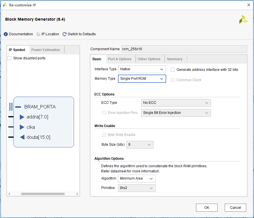
Figure 8.1 ROM setting 1
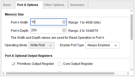
Figure 8.2 ROM setting 2
Click OK button to generate ROM
The third step: instantiate ROM
| reg [15:0] rom_q;
rom_256x16 rom_256x16_inst ( .clka (sys_clk), .addra (sw), .douta (rom_q) ); |
The fourth step: create *.coe file and initialize ROM
The .coe file for this experiment was generated based on matlab2018. The *.m file is as follows:
| % –by Alex li–
% function : create .coe clear all; close all; clc; depth= 256; width =16; fid_s = fopen(‘test_rom.coe’, ‘w+’); fprintf(fid_s, ‘MEMORY_INITIALIZATION_RADIX = %d;\n’,width); fprintf(fid_s, ‘%s\n’, ‘MEMORY_INITIALIZATION_VECTOR =’); for i=0:depth–1 data =i*i; b=dec2hex(data); fprintf(fid_s, ‘%s’, b); fprintf(fid_s, ‘%s\n’, ‘,’); end fclose(fid_s); disp(‘=======mif file completed========’); |
The generated *.m file has a depth of 256, the width of each data is 16, and the data is the square of the depth value. *.coe file content and format are shown in Figure 8.3.
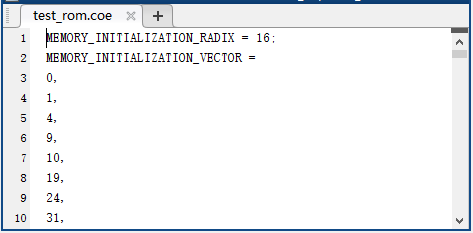
Figure 8.3 *.coe file content
Under the Sources window of the Vivado interface, expand the Design Sources folder, double-click to open the ROM created previously, enter the setting interface, under the Other Options window, select the check box Load Init Flie, and click Browse to add the generated *.coe file, such as shown in Figure 8.4, click the OK button to complete the initialization of the ROM.
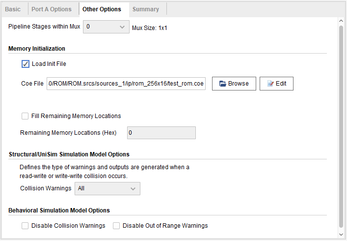
Figure 8.4 Initialize ROM
The fifth step: comprehensive design
Instantiate all modules and integrate them into the top-level file. Refer to experiment 7 to complete the program design.
8.4 Experiment Verification
The first step: add constraints and assign pins
The pin assignment is the same as that of experiment 7, refer to experiment 7 for more information.
The second step: run the implementation, generate bitstream files, and verify the board
After successfully downloading the generated programmable bitstream file to the Zynq_7030 development board, the experimental phenomenon is shown in Figure 8.5.
When the DIP switch is 0000_0011 (3 in decimal), which means the content in the third byte of the rom will be read out. The segment display illustartes 9 and is the square of 3, which is consistent with the data have been stored.
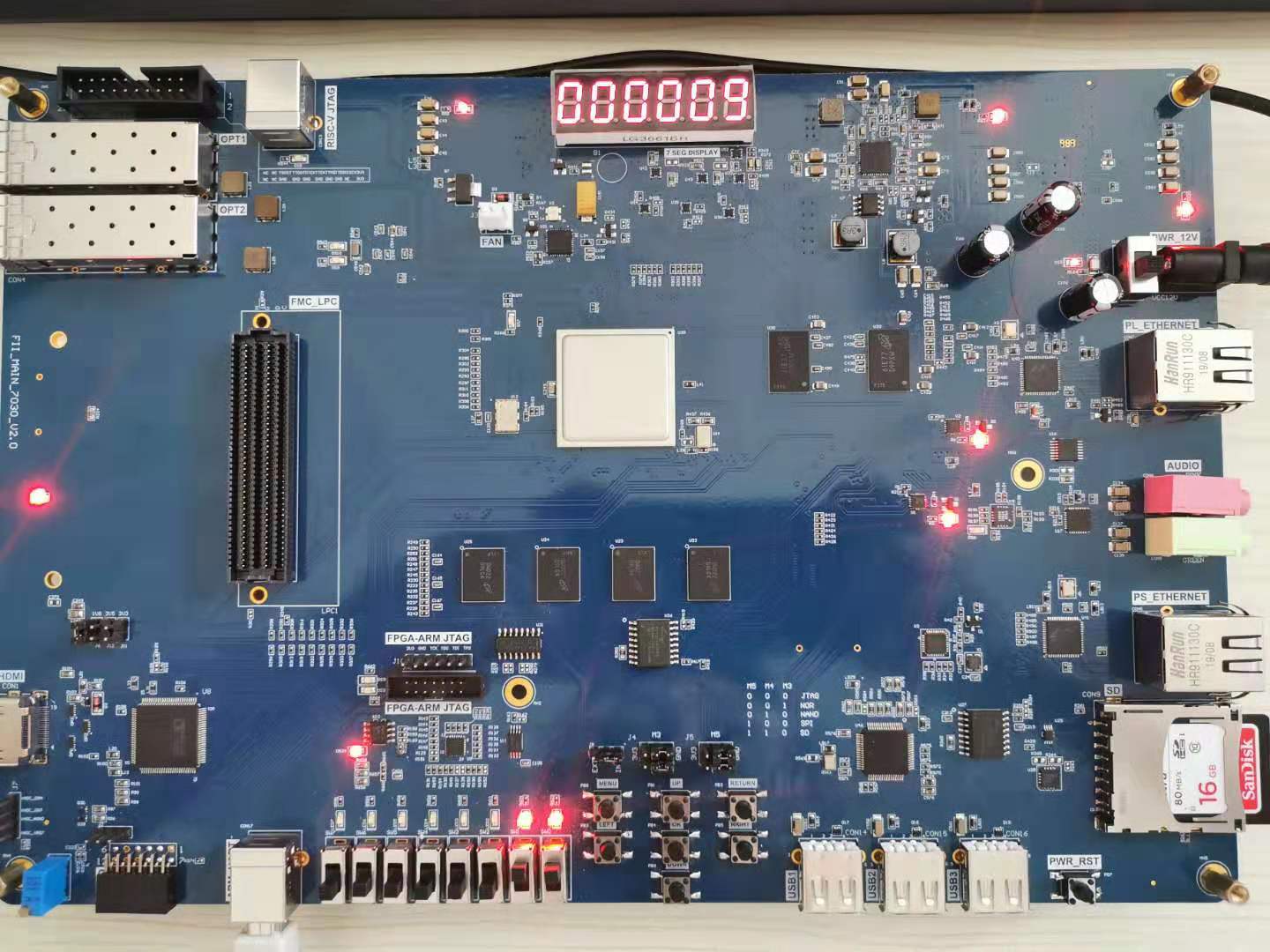
Figure 8.5 Experimental phenomenon of ROM usage