Ethernet Experiment Information received by PC from FPGA
FII-PE7030 FPGA Board Based FPGA Products FPGA Tutor

Ethernet work mechanism, the relationship between different interface types (MII, GMII, RGMII), leanrn how to transmission and reception of data, zynq xc7z030 board – FII-PE7030 Experiment 13

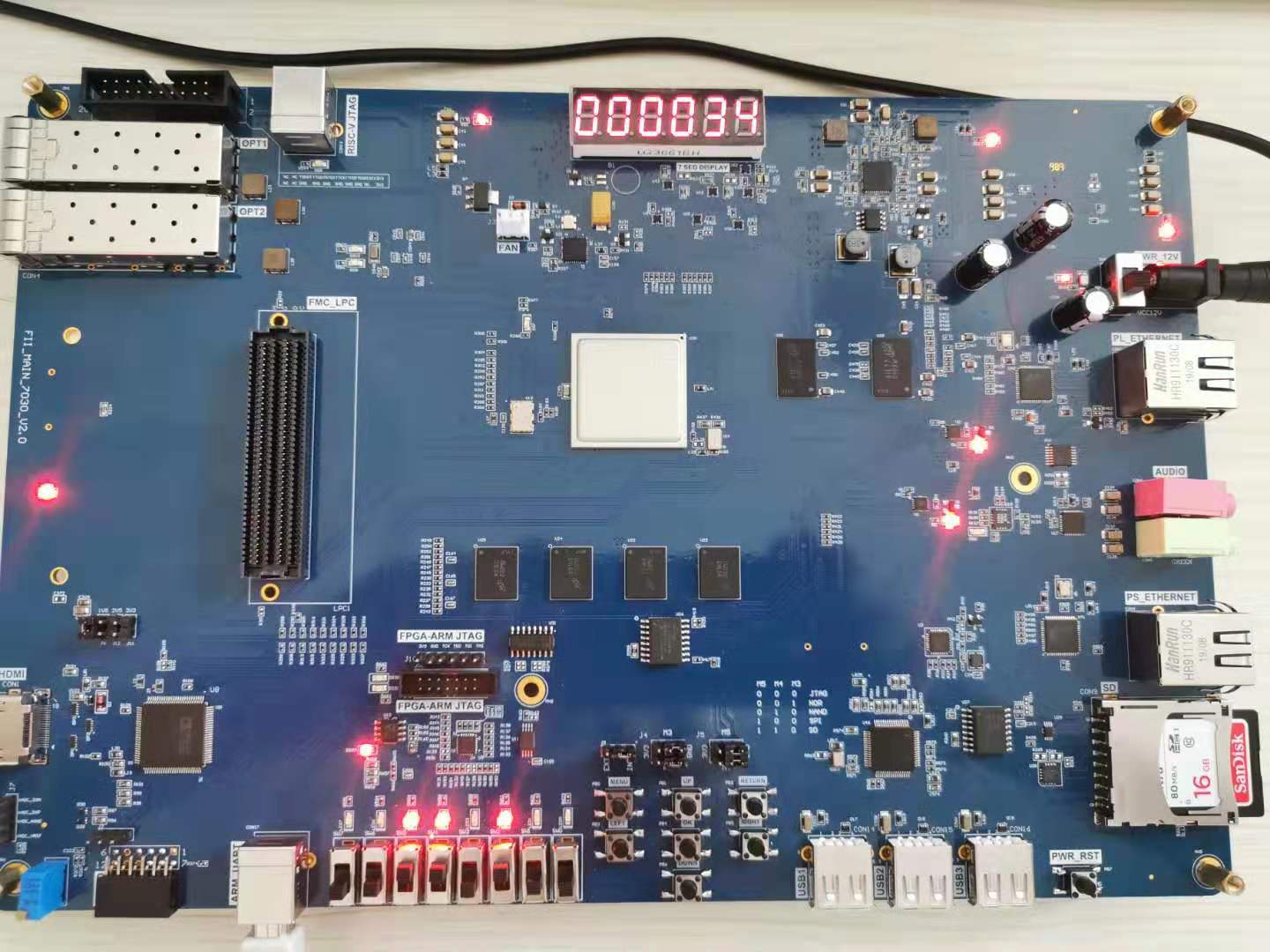
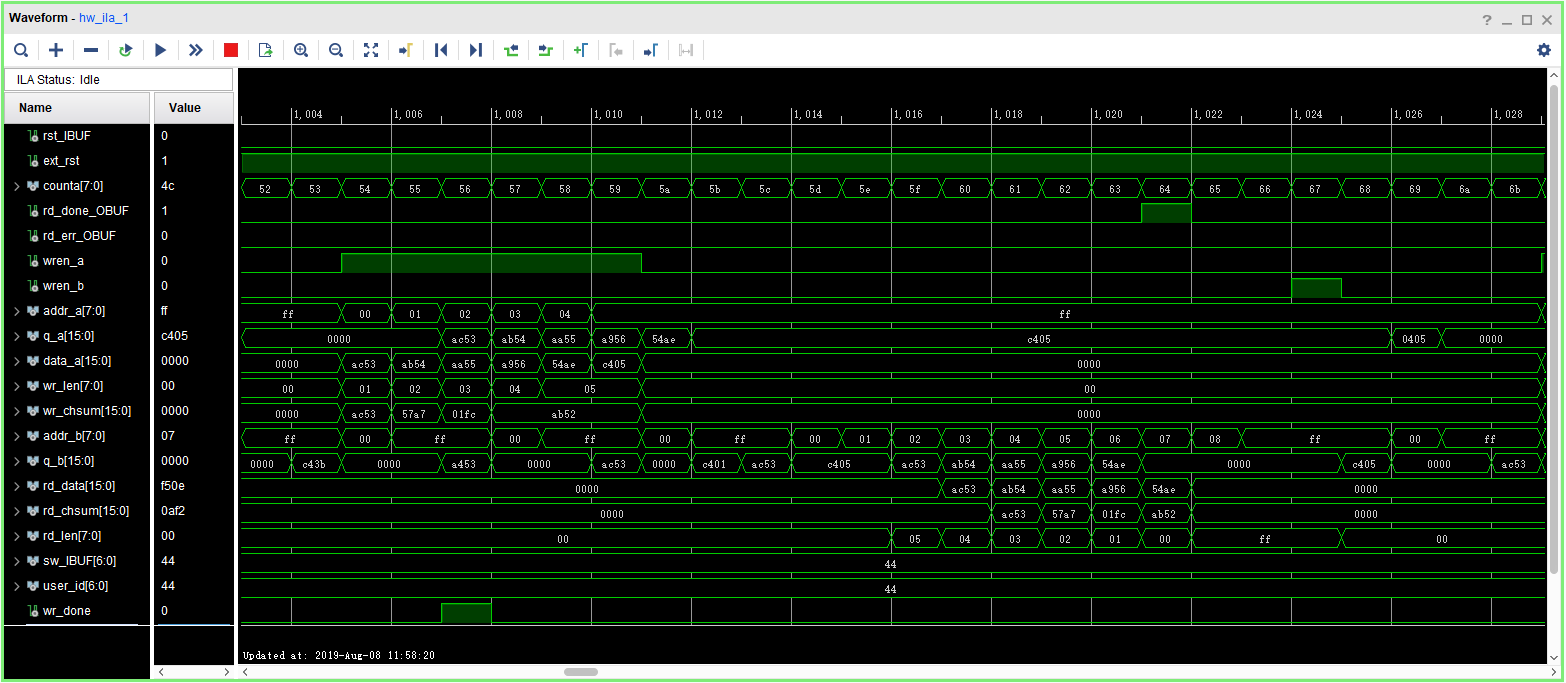
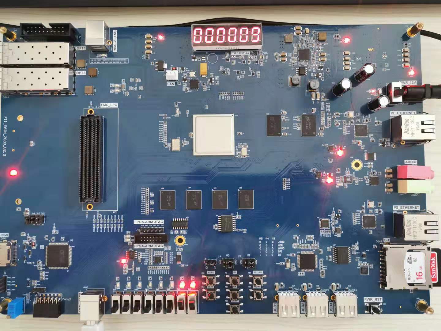
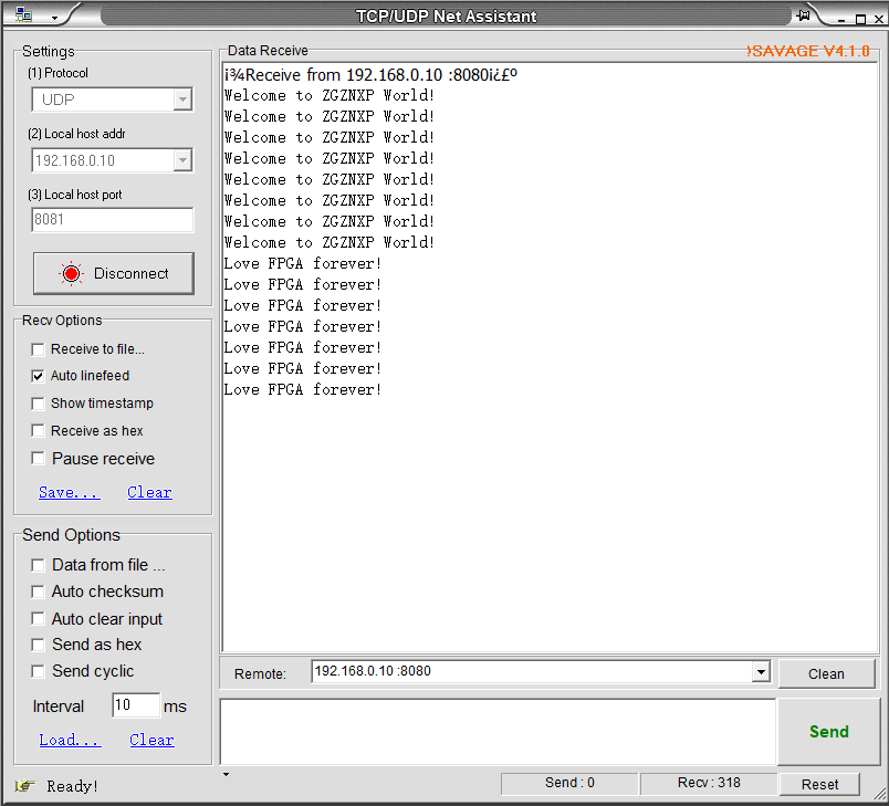
Experiment 13 Ethernet 13.1 Experiment Objective Understand what Ethernet and how it works Familiar with the relationship between different interface types (MII, GMII, RGMII) and their advantages and disadvantages (here uses RGMII) Combine the development board to complete the transmission and reception of data and verify it 13.2 Experiment Implement Perform a loopback test to check if the hardware is working properly. Perform data receiving verification Perform data transmission verification 13.3 Experiment 13.3.1 Introduction to Experiment Principle Ethernet is a baseband LAN technology. Ethernet communication is a communication method that…

Read More
zynq xc7z030 board – FII-PE7030 Experiment 12 - HDMI display (color strip)
Experimental Manuals FII-PE7030 FPGA Board Based FPGA Products FPGA Tutor

IIC protocol knowledge,Learn HDMI theory – zynq xc7z030 board – FII-PE7030 Experiment 12 – HDMI Experiment

Experiment 12 HDMI Experiment 12.1 Experiment Objective Review IIC protocol knowledge Learn HDMI theory 12.2 Experiment Implement Through the HDMI interface, different image contents are displayed on the screen. 12.3 Experiment 12.3.1 Introduction to HDMI Interface and ADV7511 Chip Image display processing has always been the focus of FPGA research. At present, the image display mode is also developing. The image display interface is also gradually transitioning from the old VGA interface to the new DVI or HDMI interface. HDMI (High Definition Multimedia Interface) is a digital video/audio interface technology.…

Read More
IIC transmission experimental phenomenon
Experimental Manuals FII-PE7030 FPGA Board Based FPGA Products FPGA Tutor

asynchronous IIC bus, and the IIC communication protocol, reading and writing EEPROM – zynq xc7z030 board – FII-PE7030 Experiment 11 – IIC Protocol Transmission

Experiment 11 IIC Protocol Transmission 11.1 Experiment Objective Learning the basic principles of asynchronous IIC bus, and the IIC communication protocol Master the method of reading and writing EEPROM Joint debugging using logic analyzer 11.2 Experiment Implement Correctly write a number to any address in the EEPROM (this experiment writes to the register of 8’h03 address) through the FPGA (here changes the written 8-bit data value by (SW7~SW0)). After writing in successfully, read the data as well. The read data is displayed directly on the segment display. Download the program…

Read More
Use Dual-port RAM to Read and Write Frame Data
Experimental Manuals FII-PE7030 FPGA Board Based FPGA Products FPGA Tutor

zynq xc7z030 board – FII-PE7030 Experiment 9 – Use Dual-port RAM to Read and Write Frame Data

Experiment 9 Use Dual-port RAM to Read and Write Frame Data 9.1 Experiment Objective Learn to configure and use dual-port RAM Learn to use synchronous clock to control the synchronization of frame structure Learn to use asynchronous clock to control the synchronization of frame structure Use ILA to observe the structure of a synchronized clock frame Extended the use of dual-port RAM Design the use of three-stage state machine Experiment Implement Use ILA to observe the structure of a synchronized clock frame Extended the use of dual-port RAM Design the…

Read More
Experimental phenomenon of ROM usage
Experimental Manuals FII-PE7030 FPGA Board Based FPGA Products FPGA Tutor

zynq xc7z030 board – FII-PE7030 Experiment 8 – Use of ROM, Study the format of *.coe and how to edit *.coe file to configure the contents of ROM

    Experiment 8 Use of ROM 8.1 Experiment Objective Study the usage of internal memory block of FPGA Study the format of *.coe and how to edit *.coe file to configure the contents of ROM Learn to use RAM, read and write RAM 8.2 Experiment Implement Design 16 outputs ROM, address ranging 0-255 Interface 8-bit switch input as ROM’s address Segment display illustartes the contents of ROM and require conversion of hexadecimal to BCD output. 8.3 Experiment 8.3.1 Program Design The first step: the establishment of the main program…

Read More
FPGA for Beginners FPGA Tutor Pocket Boards

LED_shifting , Frequency Divider Verilog HDL Code using the development software Quartus, FPGA pin assignment – FPGA Board Beginner Tutorial – FII-PRA006 Experiment 1

Experiment 1 LED shifting 1.1 Experiment Objective Practice using the development software Quartus, the building of new projects, and the use of system resources IP Core; Proficiency practice in the writing of Verilog HDL programs to develop a fine code writing style; Master the design of the frequency divider to realize the design of LED shifting; Mange FPGA pin assignment according to the schematics, and verify it though programming the development board; Observe and summarize the experiment result 1.2 Experiment Implement All LEDs are lit up when pressing self-defined reset…

Read More