AD9361
The AD9361 is a high performance, highly integrated radio frequency (RF) Agile Transceiver™ designed for use in 3G and 4G base station applications. It is developed and manufactured by Analog Devices company.
Its programmability and wideband capability make it ideal for a broad range of transceiver applications. The device combines a RF front end with a flexible mixed-signal baseband section and integrated frequency synthesizers, simplifying design-in by providing a configurable digital interface to a processor. The AD9361 receiver LO operates from 70 MHz to 6.0 GHz and the transmitter LO operates from 47 MHz to 6.0 GHz range, covering most licensed and unlicensed bands. Channel bandwidths from less than 200 kHz to 56 MHz are supported.
The two independent direct conversion receivers have state-of-the-art noise figure and linearity. Each receive (RX) subsystem includes independent automatic gain control (AGC), dc offset correction, quadrature correction, and digital filtering, thereby eliminating the need for these functions in the digital baseband. The AD9361 also has flexible manual gain modes that can be externally controlled. Two high dynamic range analog-to-digital converters (ADCs) per channel digitize the received I and Q signals and pass them through configurable decimation filters and 128-tap finite impulse response (FIR) filters to produce a 12-bit output signal at the appropriate sample rate.
The transmitters use a direct conversion architecture that achieves high modulation accuracy with ultralow noise. This transmitter design produces a best in class TX error vector magnitude (EVM) of <−40 dB, allowing significant system margin for the external power amplifier (PA) selection. The on-board transmit (TX) power monitor can be used as a power detector, enabling highly accurate TX power measurements.
The fully integrated phase-locked loops (PLLs) provide low power fractional-N frequency synthesis for all receive and transmit channels. Channel isolation, demanded by frequency division duplex (FDD) systems, is integrated into the design. All VCO and loop filter components are integrated. The core of the AD9361 can be powered directly from a 1.3 V regulator. The IC is controlled via a standard 4-wire serial port and four real-time input/output control pins. Comprehensive power-down modes are included to minimize power consumption during normal use. The AD9361 is packaged in a 10 mm × 10 mm, 144-ball chip scale package ball grid array (CSP_BGA).
Applications
- Point to point communication systems
- Femtocell/picocell/microcell base stations
- General-purpose radio systems
AD9361 Features and Benefits
- RF 2 × 2 transceiver with integrated 12-bit DACs and ADCs
- TX band: 47 MHz to 6.0 GHz
- RX band: 70 MHz to 6.0 GHz
- Supports TDD and FDD operation
- Tunable channel bandwidth: <200 kHz to 56 MHz
- Dual receivers: 6 differential or 12 single-ended inputs
- Superior receiver sensitivity with a noise figure of 2 dB at 800 MHz LO
- RX gain control
- Real-time monitor and control signals for manual gain
- Independent automatic gain control
- Dual transmitters: 4 differential outputs
- Highly linear broadband transmitter
- TX EVM: ≤−40 dB
- TX noise: ≤−157 dBm/Hz noise floor
- TX monitor: ≥66 dB dynamic range with 1 dB accuracy
- Integrated fractional-N synthesizers
- 2.4 Hz maximum local oscillator (LO) step size
- Multichip synchronization
- CMOS/LVDS digital interface
For more Analog Device information, Please check
https://www.analog.com/en/products/ad9361.html#product-overview
Our products that based on AD9361
AD-FMCOMMS3-EBZ Board $379 Compatible FII- BD9361 – AD9361 Development Board, AD9361 Software Development Kit – compatible AD9361 RF Transceiver™ ZedBoard
FII-BD9361 Features and Benefits
-
Software tunable across wide frequency range : TX :47 MHz to 6 GHz RX:70 MHz to 6 GHz
-
Software tunable bandwidth: 200 kHz to 56 MHz.
-
Software tunable TX Power and RX Dynamic Range:TX>80dB RX>70dB
-
Powered up from single standard FMC connector
-
Supports MIMO radio,2 ways TX and 2 ways RX(Max 4T4R by RF Switches configuration)
-
Supports FII-7030 and other standard FMC Connector Platform software radio application
-
TX Power higher, Broadband flatness is better.
FII-BD9361 Features
We support all features of AD-FMCOMMS3-EBZ such as:
TX band: 47 MHz to 6.0 GHz
RX band: 70 MHz to 6.0 GHz
Bandwidth Adjustment Range: 200 kHz to 56 MHz
Low noise figure: 2dB NF(noise figure/800MHz )
LO ,RX Gain Control,AGC
2.4Hhz local oscillator (LO) step
For more information, please check ad9361 introduction.
FII-BD9361 Applications
-
-
- General purpose design for any software-designed radio application
- MIMO radio
- Point to point communication systems
- Femtocell/picocell/microcell base stations
- USRP
- 3G/4G signal and protocol analysis
- WiFi
- ISM
-
3. Compatible Boards
AD-FMCOMMS3-EBZ (FII-BD9361 the same as )
(https://www.analog.com/en/design-center/evaluation-hardware-and-software/evaluation-boards-kits/eval-ad-fmcomms3-ebz.html#eb-overview)
4. Support Boards
ZC702
ZC706
Zedboard
FII-PE7030
5. User Guide : (FII-BD9361 can use it )
https://wiki.analog.com/resources/eval/user-guides/ad-fmcomms3-ebz
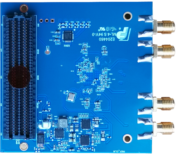
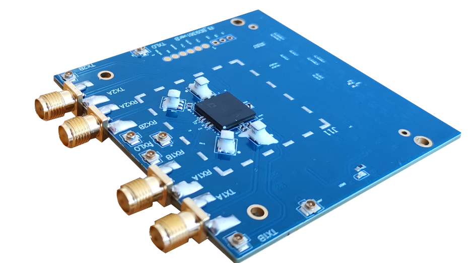
FII-BD9361 is developed by Fraser Innovation INC. It is absolutely compatible with AD-FMComms3-EBZ Board. The purpose of the AD-FMComms3-EBZ is to provide an RF platform to software developers, system architects, etc, who want a single platform which operates over a much wider tuning range (70 MHz – 6 GHz). It’s expected that the RF performance of this platform can meet the datasheet specifications at 2.4 GHz, but not at the entire RF tuning range that the board supports (but it will work much better than the AD-FMCOMMS2-EBZ over the complete RF frequency). We will provide typical performance data for the entire range (70 MHz – 6 GHz) which is supported by the platform.
This is primarily for system investigation and bring up of various waveforms from a software team before their custom hardware is complete, where they want to see waveforms, but are not concerned about the last 1dB or 1% EVM of performance.
You can find the user guide in above link at analog website. We will send you hardware configuration and system Scheme Diagram when you purchase this products.
4. System Scheme Diagram
![]()
5. Peripheral Interfaces

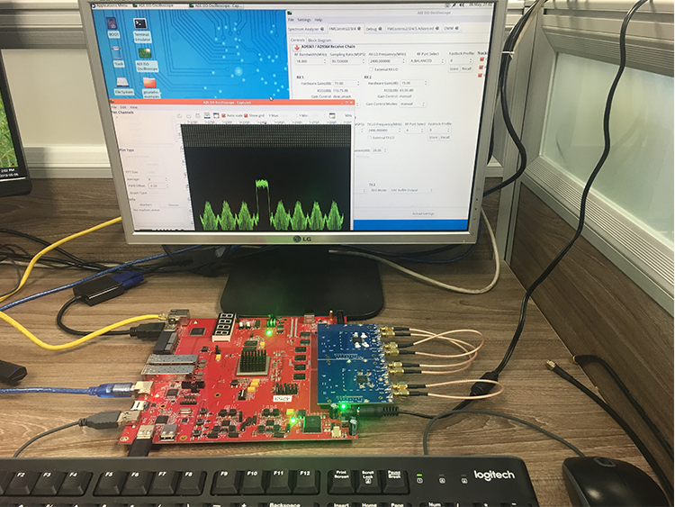
6. testing scenarios

FII-AD9361 – Test data reference (part of the project)
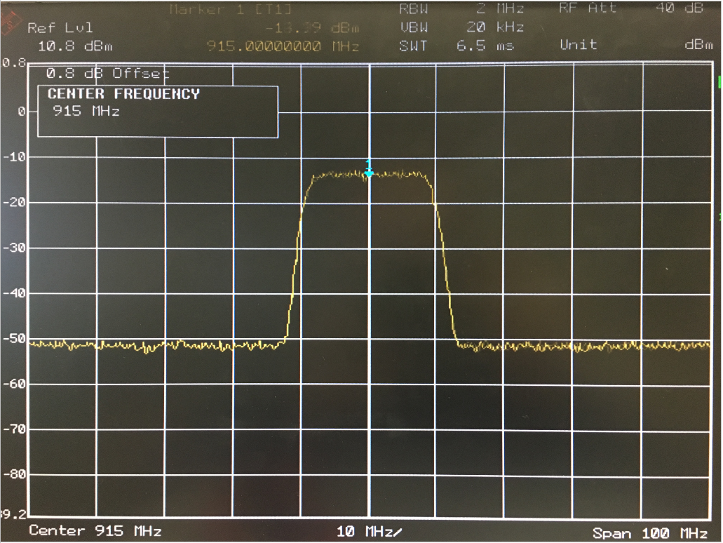
1. Output power and flatness test
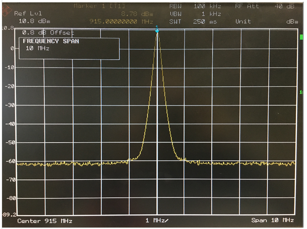
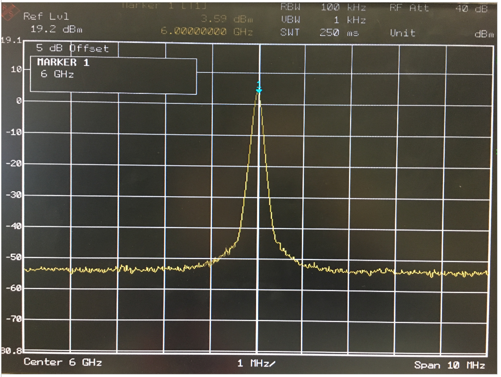
Test summary: The above picture shows some test screenshots, the frequency range covers from 70MHz to 6GHz, 150MHz to 6GHz output power 3-8dBm, high performance RF balun design guarantees high bandwidth and high flatness.
2. Phase noise test
Test summary: The above picture is a partial test screenshot, the frequency range covers from 70MHz to 6GHz, 6GHz phase noise typical value is 90dBc/1KHz, 100dBc/10KHz, perfect phase noise guarantees high quality communication test requirements.
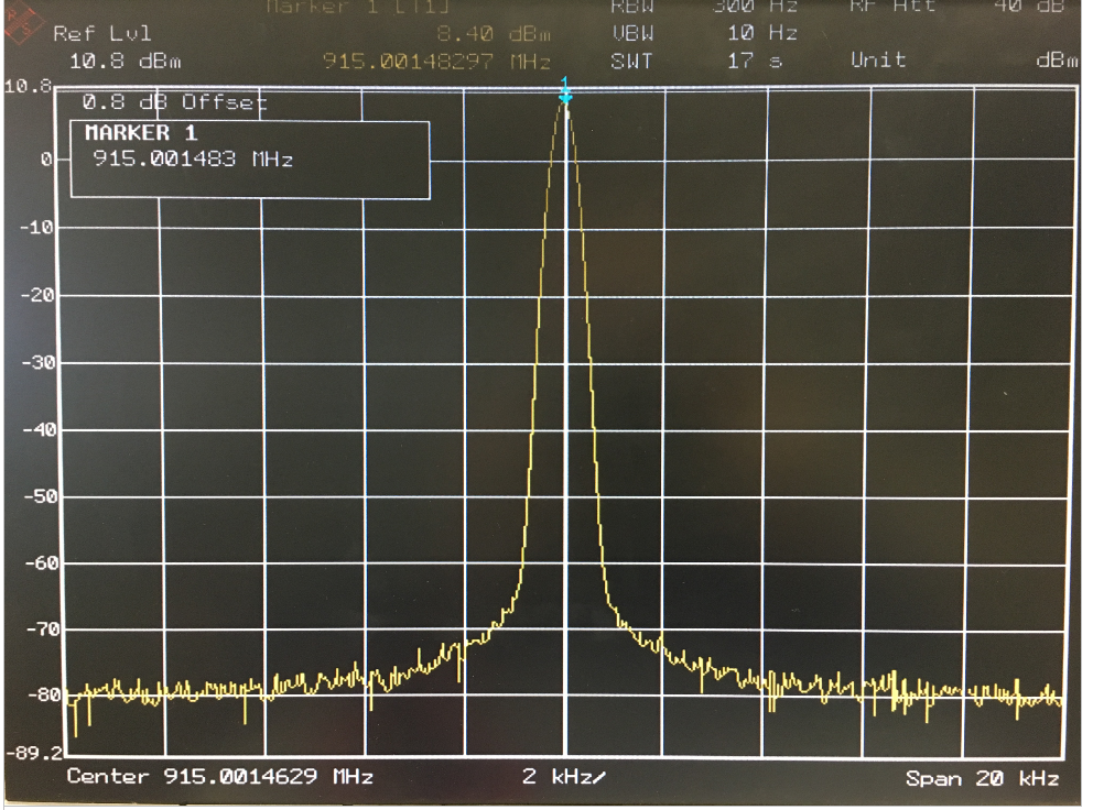
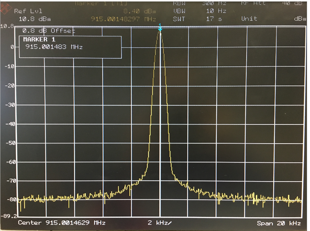
3. IQ modulation function test
Test summary: The above figure shows the spectrum signal output of QPSK modulated at 915M frequency 20M, and the IQ modulation function is normal.
For more information about our FII-BD9361 – Perfectly compatible with AD-FMCOMMS3-EBZ – Code compatible, development tool compatible, performance compatible, Smaller size and more space saving
Please click following link:
AD-FMCOMMS3-EBZ Board $379 Compatible FII- BD9361 – AD9361 Development Board, AD9361 Software Development Kit – compatible AD9361 RF Transceiver™ ZedBoard