AD9371
What is AD9371 ?
The AD9371 is a highly integrated, wideband RF transceiver offering dual channel transmitters and receivers, integrated synthesizers, and digital signal processing functions. The IC delivers a versatile combination of high performance and low power consumption required by 3G/4G micro and macro BTS equipment in both FDD and TDD applications. The AD9371 operates from 300 MHz to 6000 MHz, covering most of the licensed and unlicensed cellular bands. The IC supports receiver bandwidths up to 100 MHz. It also supports observation receiver and transmit synthesis bandwidths up to 250 MHz to accommodate digital correction algorithms.
The transceiver consists of wideband direct conversion signal paths with state-of-the-art noise figure and linearity. Each complete receiver and transmitter subsystem includes dc offset correction, quadrature error correction (QEC), and programmable digital filters, eliminating the need for these functions in the digital baseband. Several auxiliary functions such as an auxiliary analog- to-digital converter (ADC), auxiliary digital-to-analog converters (DACs), and general-purpose input/outputs (GPIOs) are integrated to provide additional monitoring and control capability.
An observation receiver channel with two inputs is included to monitor each transmitter output and implement interference mitigation and calibration applications. This channel also connects to three sniffer receiver inputs that can monitor radio activity in different bands.
The high speed JESD204B interface supports lane rates up to 6144 Mbps. Four lanes are dedicated to the transmitters and four lanes are dedicated to the receiver and observation receiver channels.
The fully integrated phase-locked loops (PLLs) provide high performance, low power fractional-N frequency synthesis for the transmitter, the receiver, the observation receiver, and the clock sections. Careful design and layout techniques provide the isolation demanded in high performance base station applications. All voltage controlled oscillator (VCO) and loop filter components are integrated to minimize the external component count.
A 1.3 V supply is required to power the core of the AD9371, and a standard 4-wire serial port controls it. Other voltage supplies provide proper digital interface levels and optimize transmitter and auxiliary converter performance. The AD9371 is packaged in a 12 mm × 12 mm, 196-ball chip scale ball grid array (CSP_BGA).
Applications
- 3G/4G micro and macro base stations (BTS)
- 3G/4G multicarrier picocells
- FDD and TDD active antenna systems
- Microwave, nonline of sight (NLOS) backhaul systems
What is Features and Benefits of AD9371 ?
- Dual differential transmitters (Tx)
- Dual differential receivers (Rx)
- Observation receiver (ORx) with 2 inputs
- Sniffer receiver (SnRx) with 3 inputs
- Tunable range: 300 MHz to 6000 MHz
- Tx synthesis bandwidth (BW) to 250 MHz
- Rx BW: 8 MHz to 100 MHz
- Supports frequency division duplex (FDD) and time division duplex (TDD) operation
- Fully integrated independent fractional-N radio frequency (RF) synthesizers for Tx, Rx, ORx, and clock generation
- JESD204B digital interface
Evaluation Kits
ADRV9371
The ADRV9371-N/PCBZ and ADRV9371-WPCBZ are radio cards designed to showcase the AD9371, a high performance wideband integrated RF transceiver intended for use in RF applications such as 4G basestation, test and measurement applications and software defined radios. The radio cards provide hardware engineers, software engineers and system architects with a single 2×2 transceiver platform for device evaluation and rapid prototyping of radio solutions. All peripherals necessary for the radio card to operate including a high efficiency switcher only power supply solution, and a high performance clocking solution are populated on the board.
Both narrow tuning range and wide tuning range options exist.
The ADRV9371-N/PCBZ is optimized for performance over a narrow tuning range1.8GHz – 2.6GHz. It will exhibit diminished RF performance on tuned RF frequencies outside of this band. This board is primarily intended to provide RF engineers with the ability to connect the AD9371 to an RF test bench (Vector Signal Analyzer, Signal Generator, etc) and achieve its optimum performance.
Fraser Innovation Inc designed a FPGA board based on AD9361 which is ADRV9371-W/PCBZ Compatible RF/IF and RFID FPGA – FII-BD9371 Board
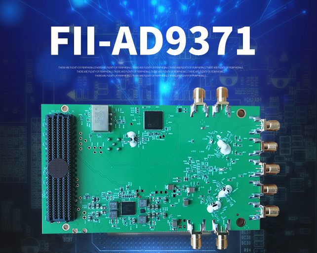
Description of FII-AD9371
FII-AD9371 (completely compatible with ADRV9371-W/PCBZ ) are radio cards designed to showcase the AD9371, a high performance wideband integrated RF transceiver intended for use in RF applications such as 4G basestation, test and measurement applications and software defined radios.
FII-BD9371 (completely compatible with ADRV9371-W/PCBZ board ) is a single board with integrated transceiver AD9371 and its supporting power supply, radio frequency and digital interface, which is a high-performance, highly integrated RF transceiver board, suitable for 3G to 5G base station and test equipment, software-defined radio SDR and other RF application fields, the programmability and broadband capabilities of the module make it an ideal choice for a variety of transceiver applications. Transceiver For Use With AD9371, AD9528, ADP5054.
2. The module sets the RF front end, mixer, frequency synthesizer and high-speed analog-to-digital conversion device to provide a configurable FMC-HPC digital interface for the processor or FPGA, thereby simplifying the design. The operating frequency range of the RF chip is 300 MHz to 6 GHz, and the single channel bandwidth range is up to 100 MHz.
The radio cards provide hardware engineers, software engineers and system architects with a single 2×2 transceiver platform for device evaluation and rapid prototyping of radio solutions. All peripherals necessary for the radio card to operate including a high efficiency switcher only power supply solution, and a high performance clocking solution are populated on the board.
- Complete Radio Card platform containing AD9371 with:
- 2 x Transmit outputs
- 2 x Receive inputs
- 2 x Observation inputs
- 1x Sniffer path
- Narrow tuning range and Wide tuning range options
- ADRV9371-W/PCBZ matched for 300MHz – 6GHz
- Complete with high efficiency power supply solution and clocking solution for AD9371
- FMC connector to Xilinx ZC706 motherboard (EK-Z7-ZC706-G).
- Powered from single FMC connector
- Includes schematics, layout, BOM, HDL, drivers and application software
For more information about FII-BD9371 (FII-AD9371), please check :