Experimental phenomenon of hexadecimal number to BCD code conversion
Experimental Manuals FII-PE7030 FPGA Products

Binary numbers to BCD (bin_to_bcd), Hexadecimal Number to BCD (hex_to_bcd) Code Conversion and Application – zynq xc7z030 board – FII-PE7030 Experiment 7

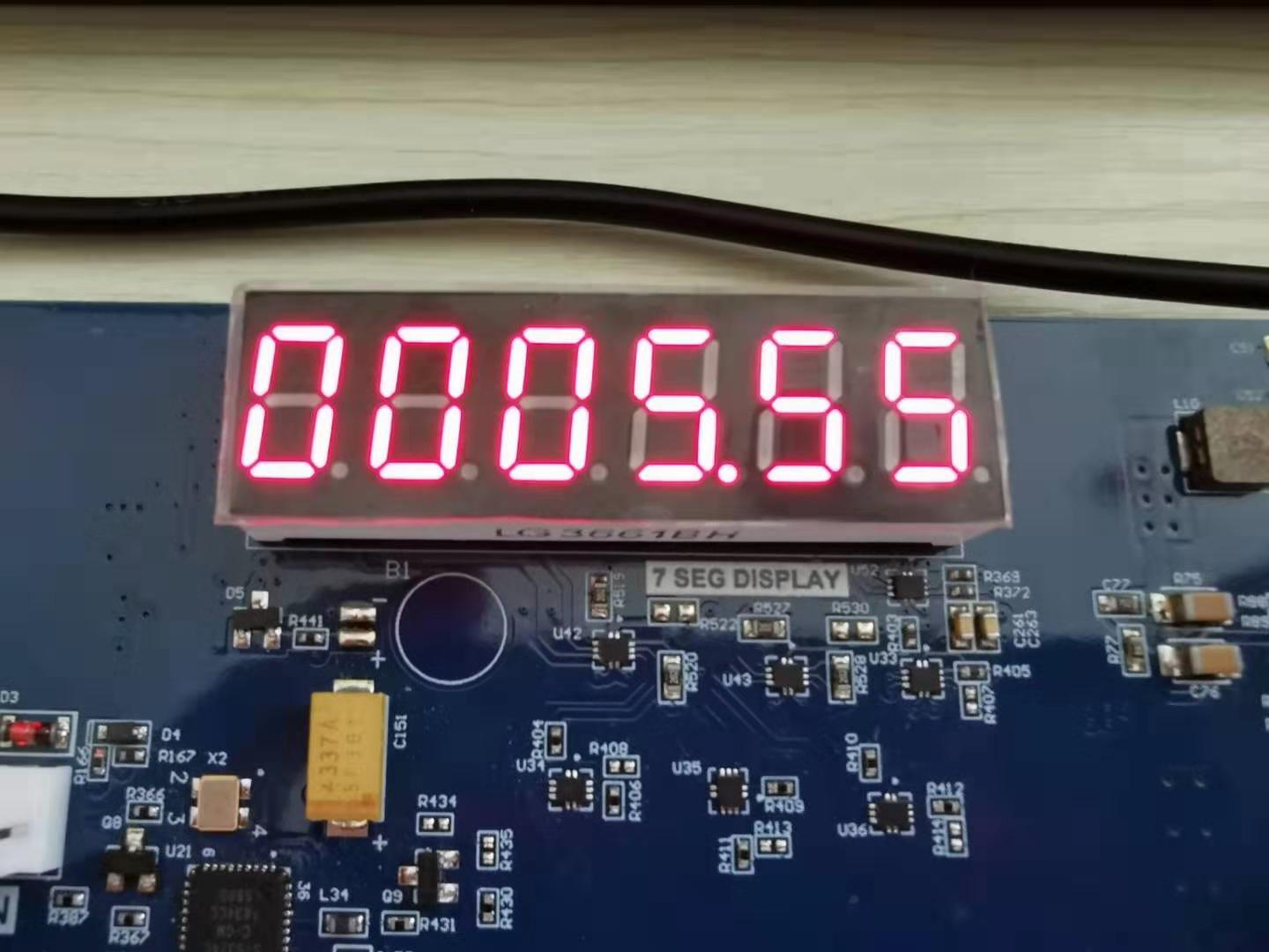
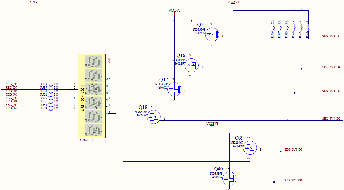
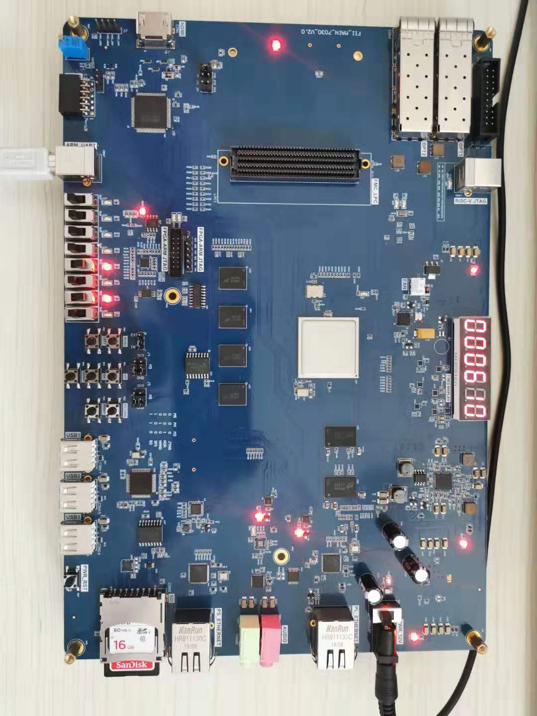
Experiment 7 Hexadecimal Number to BCD Code Conversion and Application Experiment Objective Learn to convert binary numbers to BCD (bin_to_bcd) Learn to convert hexadecimal numbers to BCD (hex_to_bcd) 7.2 Experiment Implement Combined with experiment 6, display the calculation results on the segment display. 7.3 Experiment 7.2.1 Introduction to Hexadecimal Number to BCD Code Conversion Since the hexadecimal display is not intuitive, decimal display is more widely used in real life. Human eye recognition is relatively slow, so the display from hexadecimal to decimal does not need to be too fast.…

Read More
Successfully compiled the simulation library
Experimental Manuals FII-PE7030 FPGA Board Based FPGA Products FPGA Tutor

zynq xc7z030 board – FII-PE7030 Experiment 6 – Use of Multipliers and ISIM

Experiment 6 Use of Multipliers and ISIM 6.1 Experiment Objective Learn to use multiplier Use ISIM to simulate design output 6.2 Experiment Implement 8×8 multiplier, the first input value is an 8-bit switch, and the second input value is the output of an 8-bit counter. Observe the output in ISIM 6.3 Experiment 6.3.1 Program Design The first step: the establishment of the main program framework module mult_sim( input inclk_p, input inclk_n, input [7:0] sw, output [15:0] mult_res, output reg [7:0] count ); endmodule The second step: call multiplier IP core…

Read More
zynq xc7z030 board – FII-PE7030 Experiment 4 -Digital clocl comprehensive design result
FII-PE7030 FPGA Board Based FPGA Products

zynq xc7z030 board – FII-PE7030 Experiment 5 – Digital Clock Comprehensive Experiment

Experiment 5 Digital Clock Comprehensive Experiment 5.1 Experiment Objective Review the segment display content of experiment 3, and the button debounce content of experiment 4; Combine experiment 3 and experiment 4 to design a complete adjustable digital clock; 5.2 Experiment Implement Set four push buttons (left, right, up, down); Left and right push buttons control the calibration function, switch between segment display of hour, minute and second; Up and down calibration by adding 1 and subtracting 1 to the data to be calibrated; Modular design so that the design can…

Read More
Button Debounce - Experiment results
Experimental Manuals FII-PE7030 FPGA Products

Learn button debounce principle and adaptive programming, Zynq_7030 button hardware circuit – zynq xc7z030 board – FII-PE7030 Experiment 4 – Button Debounce

Experiment 4 Button Debounce 4.1 Experiment Objective Review the design process of the shifting LED Learn button debounce principle and adaptive programming Learn the connection and use of the Zynq_7030 button hardware circuit Comprehensive application button debounce and other conforming programming 4.2 Experiment Implement Control the movement of the lit LED by pressing the button Each time the button is pressed, the lit LED moves one bit. When the left shift button is pressed, the LED moves to the left, presses the right button, and the LED moves to the…

Read More
zynq xc7z030 board
Experimental Manuals FII-PE7030 FPGA Products

BCD decoder, Display design of hexadecimal to 7 segment display decoders, Achieve digital clock display – zynq xc7z030 board – FII-PE7030 Experiment 3 – Segment Display Digital Clock Experiment

3.1 Experiment Objective Review the contents of experiment 1 and experiment 2, master the configuration of PLL, the design of frequency divider, the principle of schematics and the pin assignment of FPGA. Familiar with the design of Verilog’s tree hierarchy Study BCD decoder Display design of hexadecimal to 7 segment display decoders Achieve digital clock display 3.2 Experiment Implement The display decoder has two lower digits to display seconds, the middle two digits to display minutes, and the highest two digits to display hours. Separate the seconds, minutes, and hours…

Read More
Configuration FII-PE7030 FPGA Board Based FPGA Products Hardware Reference Guide

FII-PE7030 Hardware Reference Guide

V1.1 Fraser innovation inc FII-PE7030 Hardware Reference Guide Version Control Version Date Description V1.0 08/27/2019 Initial Release V1.1 11/19/2019 Add some SD Card Part and Potentiometer Part Copyright Notice: © 2019 Fraser Innovation Inc ALL RIGHTS RESERVED Without written permission of Fraser Innovation Inc, no unit or individual may extract or modify part of or all the contents of this manual. Offenders will be held liable for their legal responsibility. Thank you for purchasing the FPGA development board. Please read the manual carefully before using the product and make sure…

Read More