zynq xc7z030 board – FII-PE7030 Experiment 5 – Digital Clock Comprehensive Experiment
Experiment 5 Digital Clock Comprehensive Experiment
5.1 Experiment Objective
- Review the segment display content of experiment 3, and the button debounce content of experiment 4;
- Combine experiment 3 and experiment 4 to design a complete adjustable digital clock;
5.2 Experiment Implement
- Set four push buttons (left, right, up, down);
- Left and right push buttons control the calibration function, switch between segment display of hour, minute and second;
- Up and down calibration by adding 1 and subtracting 1 to the data to be calibrated;
- Modular design so that the design can be reused
- Learn to use module parameters
- Learn to use Vivado’s timing analysis function and be able to constrain the clock signal correctly
5.3 Experiment
5.3.1 Hardware Design
Refer to experiment 3 and experiment 4 for hardware design.
5.3.2 Program Design
The first step: the establishment of the main program framework (interface design)
| module adj_clock(
input inclk_p, input inclk_n, input [6:0] PB,
output [5:0] tube_sel, output [6:0] tube_seg, output point ); endmodule |
Because many push buttons are used, the 7-digit push buttons are defined in the form of PB [6: 0] bus. During the calibration time, the decimal point functions as a flag bit, which can be moved under the key drive and output separately.
The second step: system control module
Refer experiment 3.
The third step: frequency division
Refer experiment 1.
The fourth step: button debounce module
Refer experiment 4.
The fifth step: adjustable digital clock module
| always @ (posedge clk)
begin if (!rst) point_r <= 8’b1111_1110; else begin if (PB_flag[3]) point_r <= {point_r[6:0], point_r[7]}; else if (PB_flag[5]) point_r <= {point_r[0], point_r[7:1]}; end end |
For decimal point, when the reset is valid, it lights up at the lowest position. When the left shift key PB_flag [3] is valid, the decimal point is shifted one digit to the left, and when the right shift key PB_flag [5] is valid, the decimal point is shifted one digit to the right.
| //Second (top level instantiation)
dual_num_count #(.PAR_COUNTA(9), //Paramters passing .PAR_COUNTB(5) ) dual_num_count_sec ( .clk (clk), .rst (rst), .adj_add (PB_flag[1]), .adj_sub (PB_flag[6]), .adj_point (point_r[1:0]), .i_trig_f (s_f), .o_trig_f (min_f), .counta (count_secl), .countb (count_sech) ); //Calibration module module dual_num_count #(parameter PAR_COUNTA=9, parameter PAR_COUNTB=5 ) ( input clk, input rst, input adj_add, input adj_sub, input [1:0] adj_point, input i_trig_f, output reg o_trig_f, output reg [3:0] counta, output reg [3:0] countb ); always @ (posedge clk) begin if (!rst) begin counta <= 0; countb <= 0; o_trig_f <= 1’b0; end else begin o_trig_f <= 1’b0; if (adj_add) begin if (!adj_point[0]) begin if (counta == 9) counta <= 0; else counta <= counta + 1’b1; end else if(!adj_point[1]) begin if (countb == 9) countb <= 0; else countb <= countb + 1’b1; end end
else if (adj_sub) begin if (!adj_point[0]) begin if (counta == 0) counta <= 4’d9; else counta <= counta – 1’b1; end else if (!adj_point[1]) begin if (countb == 0) countb <= 4’d9; else countb <= countb – 1’b1; end end
else if (i_trig_f) begin o_trig_f <= 1’b0; if ((countb == PAR_COUNTB) && (counta == PAR_COUNTA)) begin counta <= 4’d0; countb <= 4’d0; o_trig_f <= 1’b1; end else begin if (counta == PAR_COUNTA) begin counta <= 4’d0; if (countb == PAR_COUNTB) countb <= 4’d0; else countb <= countb + 1’b1; end else counta <= counta + 1’b1; end end end end endmodule |
In the calibration part, a general module is instantiated four times, and the data of seconds, minutes, hours, and days are calibrated respectively. At the same time, the values of different internal variables are assigned in the form of parameter passing.
Take the second part as an example, enter the decimal point point [1: 0], that is, the 0th and first digits of the segment display, to illustrate the second. When the reset is valid, the counter counta = 0, countb = 0, and the output pulse (second module output pulse is the minute pulse min_f) o_trig_f = 1’b0; when the calibration signal (adj_add is a plus 1 signal and adj_sub is a minus 1 signal) is valid, the corresponding one with the decimal point lit is calibrated accordingly. Otherwise, driven by the input pulse (the input pulse of the second module is the second pulse s_f), counta increases from 0 to the parameter PAR_COUNTA (9), and countb increases from 0 to the parameter PAR_COUNTB (5). When counta = PAR_COUNTA and countb = PAR_COUNTB, both counters are cleared and the output pulse o_trig_f = 1’b1. The two counters count a total of 60, so one pulse is output in one minute.
5.4 Experiment Verification
The first step: add constraints and assign the pins
See Table 5.1 for the pin assignment.
Table 5.1 Digital clock experiment pin mapping table
| Signal Name | Network Name | FPGA Pin | Port Description |
| inclk_p | SYSCLK_P | AC13 | Input clock (differential)
200MHz |
| inclk_n | SYSCLK_N | AD13 | |
| PB[0] | GPIO_SW_0 | L9 | 7-bit push button |
| PB[1] | GPIO_SW_1 | G4 | |
| PB[2] | GPIO_SW_2 | F4 | |
| PB[3] | GPIO_SW_3 | D4 | |
| PB[4] | GPIO_SW_4 | D3 | |
| PB[5] | GPIO_SW_5 | F2 | |
| PB[6] | GPIO_SW_6 | G2 | |
| tube_sel[0] | SEG_D0 | C1 | Bit selection signal |
| tube_sel[1] | SEG_D1 | E3 | |
| tube_sel[2] | SEG_D2 | F7 | |
| tube_sel[3] | SEG_D3 | D6 | |
| tube_sel[4] | SEG_D4 | H11 | |
| tube_sel[5] | SEG_D5 | J11 | |
| tube_seg[0] | SEF_PA | J10 | Segement selection signal |
| tube_seg[1] | SEF_PB | J9 | |
| tube_seg[2] | SEF_PC | A7 | |
| tube_seg[3] | SEF_PD | B7 | |
| tube_seg[4] | SEF_PE | A8 | |
| tube_seg [5] | SEF_PF | A9 | |
| tube _seg[6] | SEF_PG | A10 | |
| tube _seg[7] | SEF_DP | B10 |
The second step: run the implementation, generate bitstream files, and verify the board
After successfully downloading the generated programmable bitstream file to the Zynq_7030 development board, the experimental phenomenon is shown in Figure 5.1.
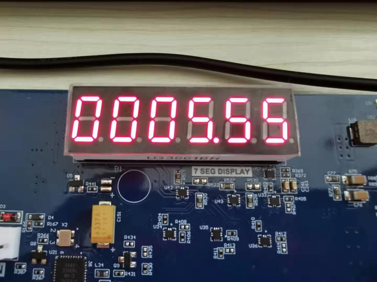
Figure 5.1 Digital clock comprehensive design result