xc7z030 board hardware resources and block diagram of ZYNQ chip
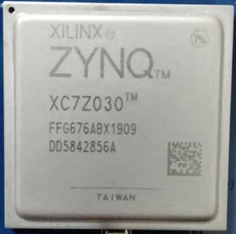
This development board uses Xilinx’s zynq7000 series chip, model XC7Z030-2FFG676I, 676-pin FPGA package.
This chip can be divided into a PS (Processor System) part and a PL (Programmable Logic) part. On the PE7030 development board, the PS and PL sections of the XC7Z030 are both equipped with a wealth of external interfaces and devices for convenience use and functional verification.
In addition, as always, the USB Cable downloader circuit is integrated on the development board. Users only need to use a USB cable to download and debug the development board.
Hardware resources:
-
-
- Two DDR3 (PL end) and four DDR3 (PS end), the model is MT41J256M16HA-125.
- Onboard three oscillators are 200MHz oscillator, 156.25MHz programmable oscillator (si570), and 33.3333MHz oscillator, providing a stable clock source for the development board
- 6-digit common anode segment display, through dynamic scanning to achieve data display;
- One channel HDMI interface, able to display colorful pictures or camera video;
- One EEPROM chip with I2C interface, model M24C08;
- Two adaptive 10M/100M/Gigabit Ethernet interfaces, one for PS and one for PL;
- 8 independent buttons, 7 programmable buttons, 1 reset button;
- An adjustable resistor can be used to simulate voltage changes;
- 8-bit DIP switch
- 8-bit LED
- One 12-pin GPIO connector that complies with the PMOD interface standard;
- One 32M serial flash chip;
- Three JTAG interfaces, two for FPGA and ARM debug interfaces, and one for JTAG debug interface for RISC-V CPU. Built-in RISC-V CPU software debugger, no external RISC-V JTAG emulator required;
- One UART asynchronous serial interface;
- Audio input interface (green), audio output interface (red);
- 4 USB interfaces, 1 for the mouse and keyboard interface, 2 for the universal serial interface;
- 1 USB (USB-B interface) to UART interface for serial communication;
- A pair of 10 Gigabit fiber interfaces;
- One SD card holder for storing operating system images and file systems;
- 1 LPC interface;
-
Basic Features of PE7030
The schematics quoted in this article are intended to highlight the key points, and the circuits that are not related to the theme (such as protection circuits or filter circuits) will be neglected. Please pay attention to that. For the source material, please refer to the attached schematic.
FPGA
As mentioned above, this development board FPGA model is XC7Z030-2FFG676I, which is Xilinx’s high-performance FPGA.
Chip resources:
| Resource | Device |
| XC7Z030-2FFG676I | |
| Logic Cells | 125K |
| Look-Up Tables | 78,600 |
| Flip-Flops | 157,200 |
| Block RAM | 9.3Mb |
| DSP Slices | 400 |
| Peak DSP Performance | 593GMACs |
| PCI Express | Gen2 x4 |
| Pin Count | 676 |
Figure 2.2 Chip Resources
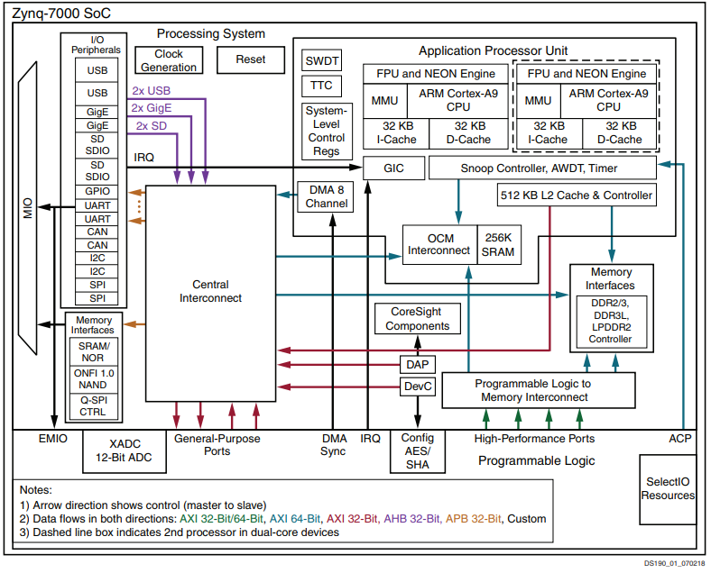
Figure 2. 3 Block Diagram of ZYNQ Chip
The main parameters of the PS system part are as follows:
– ARM dual-core CortexA9 based application processor, ARM-v7 architecture up to 1GHz
– 32KB level 1 instruction and data cache per CPU, two CPU share 512KB level 2 cache
– On-chip boot ROM and 256KB on-chip RAM
– External storage interface, support 16/32-bit DDR2, DDR3 interface
– Two Gigabit network interface cards support: divergent-aggregate DMA, GMII, RGMII, SGMII interface
– Two USB2.0 OTG interfaces, each supporting up to 12 nodes
– Two CAN2.0B bus interfaces
– Two SD card, SDIO, MMC compatible controllers
– Two SPIs, two UARTs, and two I2C interfaces
– 4 groups of 32-bit GPIO, 54 (32+22) bits as PS system I/O, 64 bits connected to PL
– High bandwidth connection within PS and from PS to PL
The chip is in a BGA package with 676 pins and a 1.0mm pin pitch. For the BGA packaged chip, the pin name is composed of “letter + number”, such as C8, E3, etc. The form of “letter + number” on the schematics represents the pins of the BGA.
For more information, please check https://fraserinnovations.com/fpga_products/fii-pe7030-hardware-reference-guide/
onlye shopping of PE7030, please go to : https://fraserinnovations.com/product/fii-pe7030-educational-platform/