Design a simple customized VGA image display, Master the principle of VGA implementation, VGA Experiment – FPGA Beginner Study Board PRA006, PRA010 Experiment 13
Experiment 13 VGA Experiment
13.1 Experiment Objective
- Master the principle of VGA implementation
- Design a simple customized VGA image display
13.2 Experiment Implement
A color bar graphic is implemented on the screen.
13.2 Experiment
13.2.1 VGA Principle
VGA (Video Graphics Array) is a computer display standard that IBM introduced in 1987 using analog signals. VGA is a low standard that is supported by most manufacturers. PCs must support the VGA standard before loading their own unique drivers.
The VGA scanning mode on the display is divided into progressive scanning and interlaced scanning: progressive scanning is scanning from the top left corner of the screen, scanning from left to right point by point, each time a line is finished, the electron beam returns to the starting position of the next line on the left of the screen. During the process the CRT blanks the electron beam, and at the end of each line, synchronizes with the line sync signal; when all the lines are scanned, a frame is formed. The field sync signal is used for field synchronization and make the scan back to the top left of the screen, while performing field blanking, start the next frame. Interlaced scanning refers to scanning every other line in the scanning of electron beams. After scanning one screen and then returning to scan the remaining lines, the interlaced display flashes quickly, which may cause eye fatigue. (This experiment uses progressive scanning). See Figure 13.1, 13.2
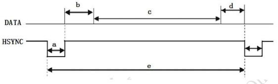
Figure 13.1 Column synchronization timing
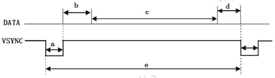
Figure 13.2 Row synchronization timing
The definition of the row timing and column timing in the VGA requires a sync pulse (a segment), a display trailing edge (b segment), and a display timing segment (c segment) and a display leading edge (d segment). VGA industry standard display mode requirements: row synchronization, column synchronization is both negative, that is, the synchronization pulse is required to be a negative pulse. According to the VGA row timing, each row has a negative row sync pulse (a segment), which is the end mark of the data line and the start mark of the next row. After the sync pulse is the display trailing edge (b segment), during the display timing segment (c segment), the monitor is bright, and the RGB data drives each pixel on the row to display one row. At the end of a row is the display leading edge (d segment). No image is projected onto the screen outside the display timing period, but a blanking signal is inserted. The sync pulse, display trailing edge, and display leading edge are all within the line blanking interval. When the blanking is valid, the RGB signal is invalid and the screen does not display data.
The column timing of VGA is basically the same as the row timing analysis.
VGA also has many display standards. In this experiment, the standard of 640×480@60 Hz is used. The standard overview is shown in Figure 13.3.
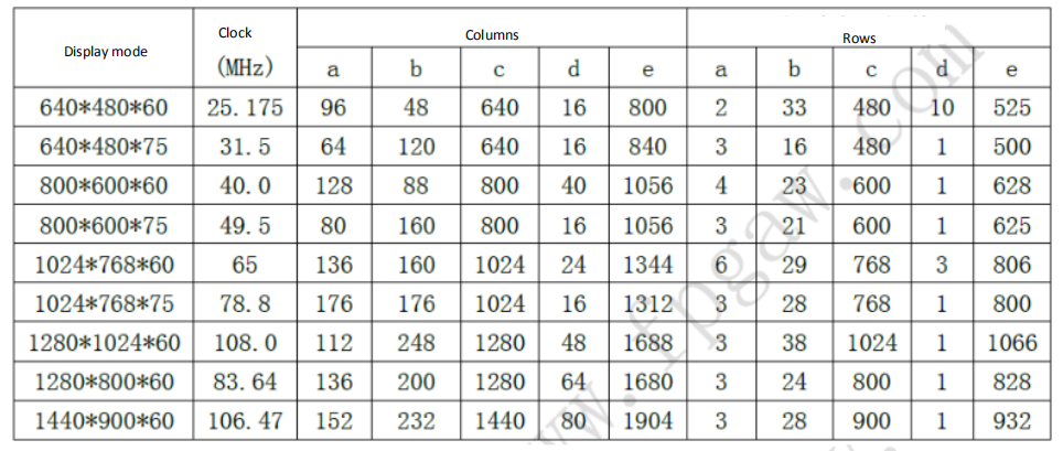
Figure 13.3 VGA display standard
Take the display standard 640*480*60 Hz of this experiment as an example. (640 is the number of columns, 480 is the number of rows, 60 Hz is the frequency to refresh a screen). Row timing: The number of rows corresponding to the screen is 525 (a + b + c + d = e segments), of which 480 (c segment) is the display row; each row has a row synchronization signal (a segment), which is 2 row periods Low level. Column timing: Each display line consists of 800 columns (a + b + c + d = e segments), where 640 (c segment) is the valid display areas, and each row has a row sync signal (a segment) of 96 column periods Low level.
13.3.2 Hardware Design

Figure 13.4 Schematics
The schematic of the VGA display is shown in Figure 13.4. The FPGA directly controls 12 data lines and two control lines, VGA_R3-R0 represents a red component, VGA_G3-G0 represents a green component, VGA_B3-B0 represents a blue component, and a line sync signal VGA_HS and a field sync signal VGA_VS.
13.3.3 Introduction to the Program
The first step: the main program framework is established
| module vga_test(
input clk, input rst, output vga_hs, output vga_vs, output [11:0] vga_data ); |
The inputs have a 50 MHz clock and a reset signal. Outputs are a line sync signal vga_has, a field sync signal vga_vs, and a 12-bit data line vga_data[11:0].
The second step: Clock frequency division Module
According to the display mode used in the experiment, the clock is output using a phase-locked loop.
The third step: control module
The main task of the control module is to display the pixels into the active area. Firstly some quantities are defined according to the display criteria.
| parameter H_SYNC = 10’d96;
parameter H_BACK = 10’d48; parameter H_DISP = 10’d640; parameter H_FRONT = 10’d16; parameter H_TOTAL = 10’d800; parameter V_SYNC = 10’d2; parameter V_BACK = 10’d33; parameter V_DISP = 10’d480; parameter V_FRONT = 10’d10; parameter V_TOTAL = 10’d525; |
The five segments with the H prefix corresponding to the column timing in Figure 13.3, the value is the number of pixels per segment, with the V prefix corresponding to the five segments of the row timing in Figure 13.3, the value is the number of rows per segment.
| reg [9:0] cnt_h;
reg [9:0] cnt_v; wire vga_en; wire data_req; assign vga_hs = (cnt_h <= H_SYNC – 1’b1) ? 1’b0 : 1’b1; assign vga_vs = (cnt_v <= V_SYNC – 1’b1) ? 1’b0 : 1’b1; assign vga_rgb = vga_en ? pixel_data : 16’d0; assign vga_en = (((cnt_h >= H_SYNC+H_BACK) && (cnt_h < H_SYNC+H_BACK+H_DISP)) &&((cnt_v >= V_SYNC+V_BACK) && (cnt_v < V_SYNC+V_BACK+V_DISP))) ? 1’b1 : 1’b0; assign data_req = (((cnt_h >= H_SYNC+H_BACK-1’b1) && (cnt_h < H_SYNC +H_BACK+H_DISP-1’b1)) && ((cnt_v >= V_SYNC+V_BACK) && (cnt_v < V_SYNC+V_BACK+V_DISP))) ? 1’b1 : 1’b0; assign pixel_xpos = data_req ? (cnt_h – (H_SYNC + H_BACK – 1’b1)) : 10’d0; assign pixel_ypos = data_req ? (cnt_v – (V_SYNC + V_BACK – 1’b1)) : 10’d0; |
This part of the content is fixed by the counter, vga_en fixes the effective area of the image. pixel_xpos and pixel_ypos give each pixel in the effective area a certain coordinate from the upper left corner to facilitate subsequent filling of the corresponding color information. Color output is only available in the active area.
The fourth step: display module
The main task of the display module is dividing the display area, and filling in the color of each block as required.
| parameter H_DISP = 10’d640;
parameter V_DISP = 10’d480; localparam WHITE = 16’b11111_111111_11111; localparam BLACK = 16’b00000_000000_00000; localparam RED = 16’b11111_000000_00000; localparam GREEN = 16’b00000_111111_00000; localparam BLUE = 16’b00000_000000_11111;
always @(posedge vga_clk or negedge sys_rst_n) begin if (!sys_rst_n) pixel_data <= 16’d0; else begin if ((pixel_xpos >= 0) && (pixel_xpos <= (H_DISP/5)*1)) pixel_data <= WHITE; else if ((pixel_xpos >= (H_DISP/5)*1) && (pixel_xpos < (H_DISP/5)*2)) pixel_data <= BLACK; else if ((pixel_xpos >= (H_DISP/5)*2) && (pixel_xpos < (H_DISP/5)*3)) pixel_data <= RED; else if ((pixel_xpos >= (H_DISP/5)*3) && (pixel_xpos < (H_DISP/5)*4)) pixel_data <= GREEN; else pixel_data <= BLUE; end end |
First, five colors, white, black, red, green, and blue, are defined. Then, according to the pixel coordinates, the display area is divided into five vertical bars, and five colors are respectively filled in.
13.4 Experiment Verification
The first step: pin assignments
See Table 13.1 for the pin assignments
Table 13.1 VGA experiment pin mapping
| Signal Name | Network Label | FPGA Pin | Port Description |
| clk | C10_50MCLK | 91 | System clock 50 MHz |
| rst | KEY3 | 10 | Reset |
| vga_data[11] | VGA_R3 | 105 | Image red component |
| vga_data[10] | VGA_R2 | 103 | |
| vga_data[9] | VGA_R1 | 101 | |
| vga_data[8] | VGA_R0 | 100 | |
| vga_data[7] | VGA_G3 | 113 | Image green component |
| vga_data[6] | VGA_G2 | 112 | |
| vga_data[5] | VGA_G1 | 111 | |
| vga_data[4] | VGA_G0 | 106 | |
| vga_data[3] | VGA_B3 | 120 | Image blue component |
| vga_data[2] | VGA_B3 | 119 | |
| vga_data[1] | VGA_B2 | 115 | |
| vga_data[0] | VGA_B1 | 114 | |
| vga_hs | VGA_HS | 98 | Horizontal synchronous signal |
| vga_vs | VGA_VS | 99 | Vertical synchronous signal |
The second step: board verification
After the pin assignment is completed, the compilation is performed, and the development board is programmed. The experimental phenomenon is shown in Figure 13. 5. The screen is divided into five vertical bars, which are white, black, red, green and blue.
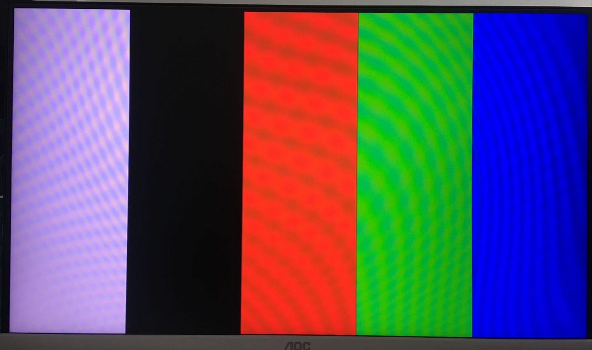
Figure 13.5 VGA experiment phenomenon