BCD_counter, The segment decoder code, Download the program into the board flash memory – FPGA for Beginner Tutorial – Experiment 3 – FII-PRA006
Experiment 3 Segment Display
3.1 Experiment Objective
- Review previous experiments, proficient practice in PLL configuration, frequency division design, and project verification;
- Learn to use the BCD code counter;
- Digital display decoding design;
- Learn to program the project into the serial FLASH of the development board;
3.2 Experiment Implement
- The segment display has two lower (right most) digits to display seconds, the middle two digits to display minutes, and the highest (left most) two digits to display hours.
- The decimal point remains off and will not be considered for the time being.
3.3 Experiment
3.3.1 Introduction to the Segment Display
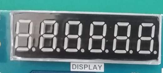
One type of segment display is a semiconductor light-emitting device. The segment display can be divided into a seven-segment display and an eight-segment display. The difference is that the eight-segment display has one more unit for displaying the decimal point, the basic unit is a light-emitting diode. The on-board segment display is a six-in-one eight-segment display as shown in Figure 3.1, and its structure is shown in Figure 3.2.
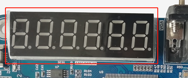
Figure 3.1 Physical picture of the segment display
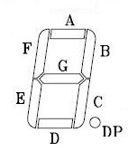
Figure 3.2 Single segment display structure
Common anode segment displays are used here. That is, the anodes of the LEDs are connected. See Figure 3.3. Therefore, the FPGA is required to control the cathode of the LED to be low level, illuminate the diode, and display the corresponding information. The six-digit common anode eight-segment display refers to the signal that controls which one is lit, which is called the bit selection signal. The content displayed by each digital segment is called the segment selection signal. The corresponding truth table is shown in Table 3.1.
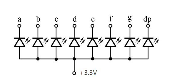
Figure 3.3 Schematics of common anode LEDs
Table 3-1 common anode eight led segment signal Truth Table
| Segment Selection Signal | DP | G | F | E | D | C | B | A |
| · | 0 | 1 | 1 | 1 | 1 | 1 | 1 | 1 |
| 0 | 1 | 1 | 0 | 0 | 0 | 0 | 0 | 0 |
| 1 | 1 | 1 | 1 | 1 | 1 | 0 | 0 | 1 |
| 2 | 1 | 0 | 1 | 0 | 0 | 1 | 0 | 0 |
| 3 | 1 | 0 | 1 | 1 | 0 | 0 | 0 | 0 |
| 4 | 1 | 0 | 0 | 1 | 1 | 0 | 0 | 1 |
| 5 | 1 | 0 | 0 | 1 | 0 | 0 | 1 | 0 |
| 6 | 1 | 0 | 0 | 0 | 0 | 0 | 1 | 0 |
| 7 | 1 | 1 | 1 | 1 | 1 | 0 | 0 | 0 |
| 8 | 1 | 0 | 0 | 0 | 0 | 0 | 0 | 0 |
| 9 | 1 | 0 | 0 | 1 | 0 | 0 | 0 | 0 |
| A | 1 | 0 | 0 | 0 | 1 | 0 | 0 | 0 |
| B | 1 | 0 | 0 | 0 | 0 | 0 | 1 | 1 |
| C | 1 | 1 | 0 | 0 | 0 | 1 | 1 | 0 |
| D | 1 | 0 | 1 | 0 | 0 | 0 | 0 | 1 |
| E | 1 | 0 | 0 | 0 | 0 | 1 | 1 | 0 |
| F | 1 | 0 | 0 | 0 | 1 | 1 | 1 | 0 |
There are two ways to display the segment display, static display and dynamic display.
Static display: Each display segment is connected with an 8-bit data line to control and maintain the displayed glyph until the next segment selection signal arrives. The advantage is that the driver is simple, and the disadvantage is that it takes up too much I/O resources.
Dynamic display: Parallel the segment selection lines of all segment display, and the digit selection line controls which digit is valid and lights up. Through the afterglow effect of the LED and the persistence effect of the human eye, the segment display appears to be continuously lit at a certain frequency. The advantage is to save I / O resources, the disadvantage is that the driver is more complicated, the brightness is not static display high.
In this experiment, the digital tube was driven by dynamic scanning.
3.3.2 Hardware Design
The schematics of the segment display is shown in Figure 3.4. The anode is connected to VCC through the P-channel field effect transistor. Therefore, when the bit selection signal SEG_3V3_D[0:5] is low level 0, the FET is turned on, the anode of the segment display is high level; the cathode (segment selection signal) SEG_PA, SEG_PB, SEG_PC, SEG_PD, SEG_PE, SEG_PF, SEG_PG, SEG_DPZ are directly connected to the FPGA and directly controlled by the FPGA. Therefore, when the bit selection signal is 0, and the segment selection signal is also 0, the segment display is lit.
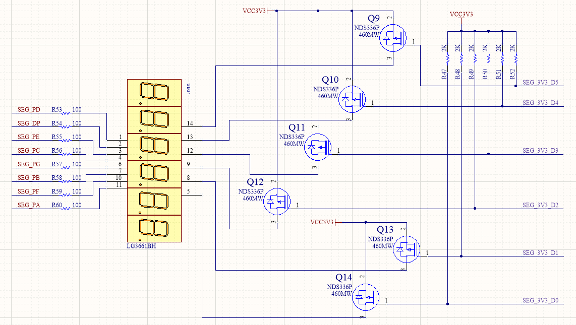
Figure 3.4 Schematics of segment display
3.3.3 Program Design
3.3.3.1 System Block Diagram
The segment display system block diagram is shown in Figure 3.5.
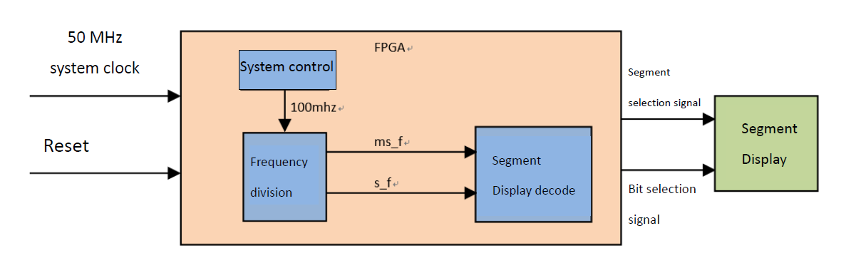
Figure 3.5 Segment display system block diagram
The top-level module RTL view is shown in Figure 3.6.
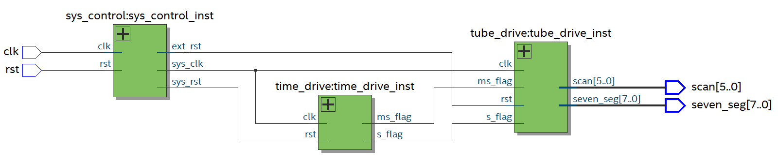
Figure 3.6 RTL view
3.3.3.2 Introduction to Program
The first step: the establishment of the main program framework (interface design)
module BCD_counter (

input clk,

input rst,

output [7:0] seven_seg,

output [5:0] scan

);

endmodule
The input signal has a clock and a reset signal, and the output signal are a segment selection signal seven_seg and a new signal scan.
The second step: system control module
//Instantiate PLL
PLL	PLL_inst
(
	.areset				(1'b0),
	.inclk0				(clk),
	.c0					(sys_clk),
	.locked				(locked)
);

//Reset signal
always @ (posedge sys_clk)
begin
	sys_rst <= !locked;
	ext_rst <= rst;
end
In the first sub-module (system control module), the input clock is the system 50 MHz clock, and a 100MHz is output through the phase-locked loop as the working clock of the other sub-modules. The phase-locked loop lock signal is inverted as the system reset signal. The button is reset to be used as an external hardware reset signal.
The third step: the frequency division module
Referring to previous experiments, a millisecond pulse signal and a second pulse signal are output as input signals of the segment display driving module.
The fourth step: segment display driver module
- Counting section
The counting part is similar to the frequency dividing module. It is timed by the second pulse signal for 60 seconds, 60 minutes, 24 hours, and when the time reaches 23 hours, 59 minutes and 59 seconds, the counters are all cleared, which is equivalent to one day.
- Segment display dynamic scanning part
reg    [3:0]    count_sel;
reg    [2:0]    scan_state;
always @ (posedge clk)
begin
	if (rst) begin
		scan	    	<= 6'b111_111;
		count_sel 	<= 4'd0;
		scan_state	<= 0;
	end
	else case (scan_state)
		0	:
		begin
			scan		<= 6'b111_110;
			count_sel	<= counta;
			if (ms_f)
				scan_state <= 1;
		end

		1	:
		begin
			scan		<= 6'b111_101;
			count_sel	<= countb;
			if (ms_f)
				scan_state	<= 2;
		end

		2	:
		begin
			scan		<= 6'b111_011;
			count_sel	<= countc;
			if (ms_f)
				scan_state <= 3;
		end

		3	:
		begin
			scan		<= 6'b110_111;
			count_sel	<= countd;
			if (ms_f)
				scan_state <= 4;
		end

		4	:
		begin
			scan		<= 6'b101_111;
			count_sel	<= counte;
			if (ms_f)
				scan_state <= 5;
		end

		5	:
		begin
			scan <= 6'b011_111;
			count_sel	<= countf;
			if (ms_f)
				scan_state <= 0;
		end
		default	:	scan_state <= 0;
	endcase
end
The dynamic scanning of the segment display is realized by the state machine. A total of six segment display require six states. The state machine scan_state[2:0] is defined, and the corresponding content count_sel is displayed in different states. At reset, all six segment display are extinguished and jump to the 0 state. The segment display is dynamically scanned in 1 millisecond time driven by a millisecond pulse:
In the 0 state, the 0 segment display is lit, and the ones digit of the second is displayed;
In the 1 state, the first segment display is lit, and the tens digit of the second is displayed;
In the 2 state, the second segment display is lit, and the ones digit of the minute is displayed;
In the 3 state, the third segment display is lit, and the tens digit of the minute is displayed;
In the 4 state, the fourth segment display is lit, and the ones digit of the hour is displayed;
In the 5 state, the fifth segment display is lit, and the tens digit of the hour is displayed
The fifth step: segment display segment code section
always @ (*)
begin
	case (count_sel)
		0	:	seven_seg_r <= 7'b100_0000;
		1	:	seven_seg_r <= 7'b111_1001;
		2	:	seven_seg_r <= 7'b010_0100;
		3	:	seven_seg_r <= 7'b011_0000;
		4	:	seven_seg_r <= 7'b001_1001;
		5	:	seven_seg_r <= 7'b001_0010;
		6	:	seven_seg_r <= 7'b000_0010;
		7	:	seven_seg_r <= 7'b111_1000;
		8	:	seven_seg_r <= 7'b000_0000;
		9	:	seven_seg_r <= 7'b001_0000;
		default : seven_seg_r <= 7'b100_0000;
	endcase
end
Referring to Table 3.1, the characters to be displayed are associated with the segment code, the decimal point is set high to extinguish, and then the final segment selection signal output is composed in a spliced form.
3.4 Application and verification of Flash_memory
The first step: pin assignment
Pin assignments are shown in Table 3.2.
Table 3.2 Segment display pin mapping
| Signal Name | Network Label | FPGA Pin | Port Description |
| clk | C10_50MCLK | 91 | Input Clock |
| rst | KEY3 | 10 | Reset |
| scan[5] | SEG_3V3_D5 | 124 | Bit selection 5 |
| scan[4] | SEG_3V3_D4 | 127 | Bit selection 4 |
| scan[3] | SEG_3V3_D3 | 129 | Bit selection 3 |
| scan[2] | SEG_3V3_D2 | 141 | Bit selection 2 |
| scan[1] | SEG_3V3_D1 | 142 | Bit selection 1 |
| scan[0] | SEG_3V3_D0 | 136 | Bit selection 0 |
| seven_seg[7] | SEG_PA | 128 | Segment selection 7 |
| seven_seg[6] | SEG_PB | 135 | Segment selection 6 |
| seven_seg[5] | SEG_PC | 138 | Segment selection 5 |
| seven_seg[4] | SEG_PD | 126 | Segment selection 4 |
| seven_seg[3] | SEG_PE | 125 | Segment selection 3 |
| seven_seg[2] | SEG_PF | 133 | Segment selection 2 |
| seven_seg[1] | SEG_PG | 137 | Segment selection 1 |
| seven_seg[0] | SEG_DP | 132 | Segment selection 0 |
The second step: compilation
The third step: solidify the program to Flash
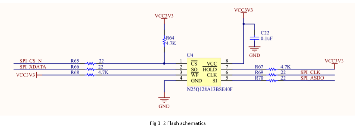
Onboard Flash (N25Q128A) is a serial Flash chip that can store 128Mbit of content, which is more than enough in the engineering learning process. The schematics of the Flash is shown in Figure 3.7.
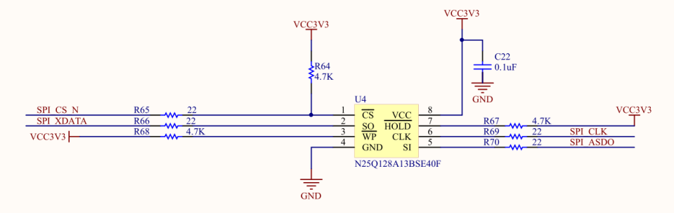
Figure 3.7 Schematics of flash
The function of Flash is to save the program on the development board. After the power is off, the program will not disappear. The next time the development board is powered on, it can be used directly. It is more practical in the actual learning life. Driven by the SPI_CLK clock, the FPGA Flash is programmed through the SPI_ASDO line. After repowered on, the FPGA re-reads the program to the FPGA through SPI_XDATA for testing.
The specific configuration process of Flash is as follows:
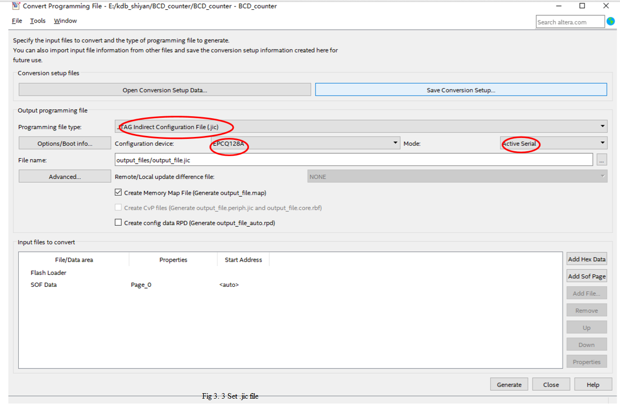
- Menu File -> Convert programming files, as shown in Figure 3.8;
- Option settings
- Select JTAG Indirect configuration File(*.Jic)
- Configuration Device:EPCQ 128A (Compatible with development board N25Q128A)
- Mode:Active serial
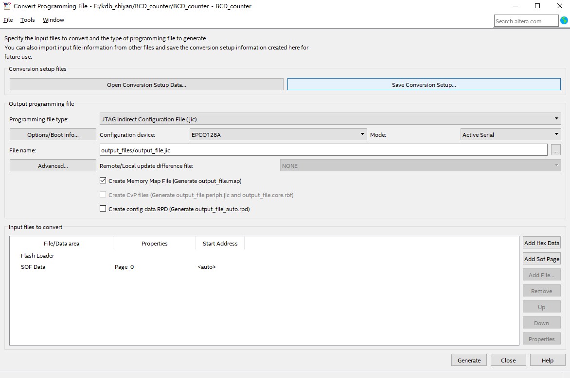
Figure 3.8 *.jic file setting
- Click the Advanced button and set it as shown in Figure 3.9.
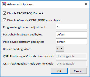
Figure 3.9 Advanced setting
- Add a conversion file, as shown in Figure 3.10.
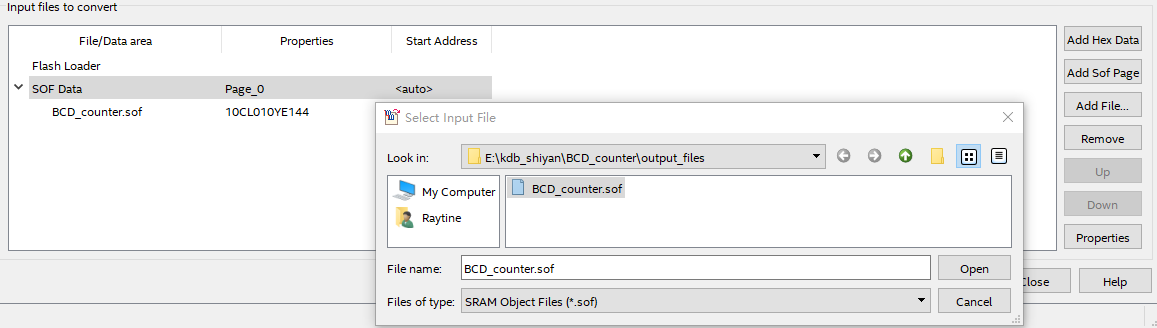
Figure 3.10 Add conversion file
- Add a device, as shown in Figure 3.11.
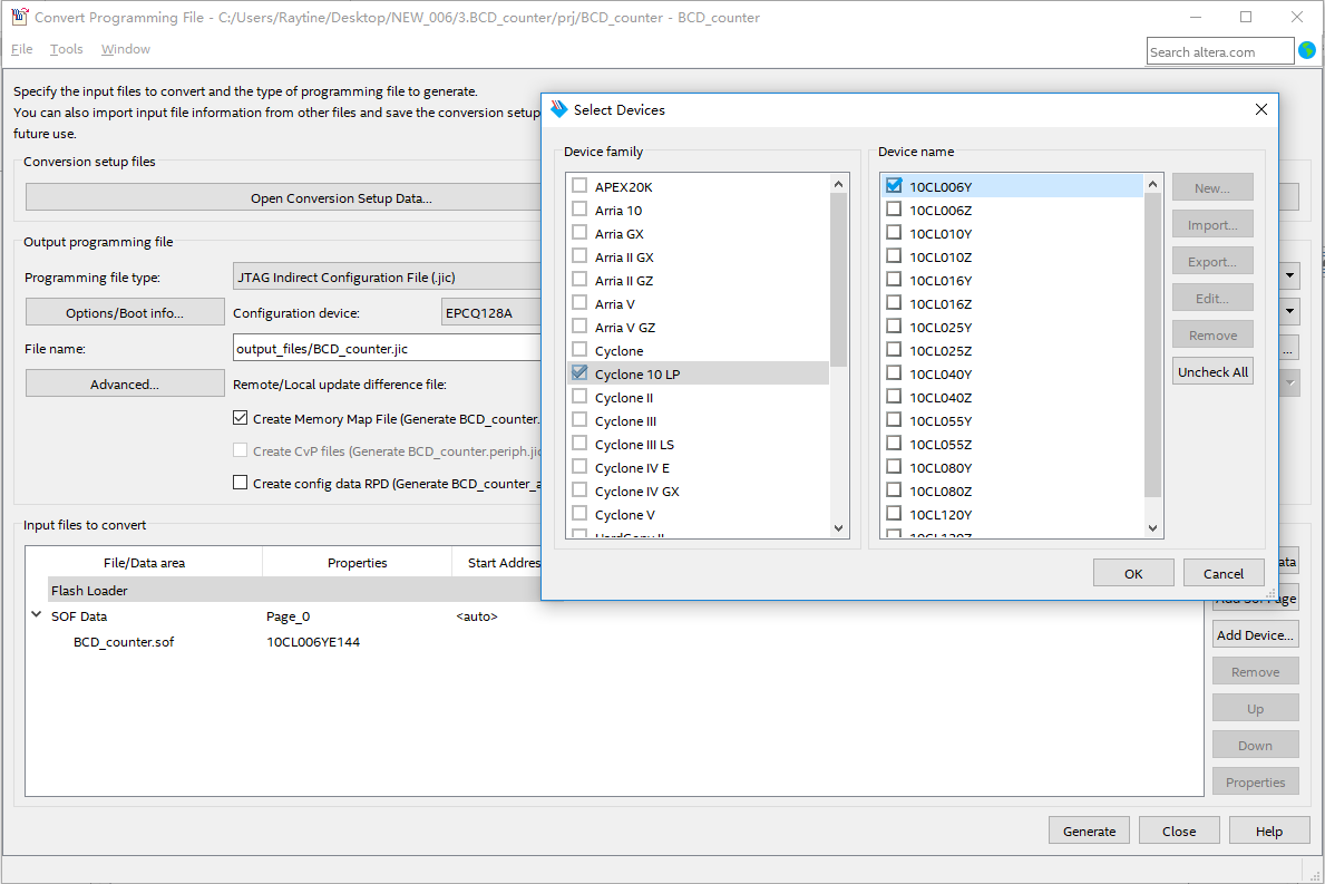
Figure 3.11 Add a device
- Click Generate to generate the BCD_counter.jic file
- Consistent with previous program verification operations, select the correct file (*.jic) to program the development board
The fourth step: power up verification
As shown in Figure 3.12, after repowered on, the FPGA automatically reads the program in Flash into the FPGA and runs it.
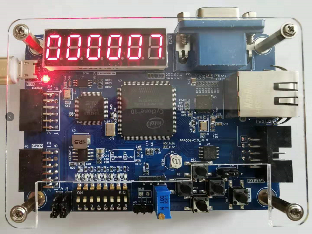
Figure 3.12 Experiment phenomenon
Old Version (2019 – Sept 1 )
————————————————————————————————————————
3.1 Experiment Objective
-
Review Experiment 1, the setting for PLL, design of frequency division, and the compilation of the code
-
Study the BCD code counter
-
Design of 7 segment decoder
-
Download the program into the board flash memory
3.2 Experiment Requirement
-
The highest two segment decoders display hours, the middle two are for minutes, and the lowest two display the seconds.
-
The decimal point will be off all the time. It will not be considered in this case.
3.3 Experiment
3.3.1 Build New Project
See Experiment 1
3.3.2 PCB Schematics

In Fig 3. 1, six 7 segment decoders are used in this experiment. Some points need to be paid attention.
-
The segment names are shown above. A, B, C, D, E, F, and G correspond to the digital tube, while DP stands for the decimal point. D0, D1, D2, D3, D4, and D5 (on the rightest part) are for the current driver.
-
They are common anode segment decoders, D0- D5 are set high or low to control the segment decoders.
-
For the main segments, A- G are lit when the input is low, that is, ‘0’ is high.
-
The segment decoder code is given as follows
5. Dynamic Scanning for human eyes. Since human eyes have visual persistence characteristics, the speed to illuminate the segment decoders is fast enough that it cannot be distinguished by naked eyes. Therefore, it can be viewed as consistent lighting instead of blinking. Like the running LED, one decoder is lit at one time, implemented in the form of low-level loop left shift
3.3.3 Experiment Procedure
-
For the frequency division design, see Experiment 1.
-
Dynamic scanning is implemented by the state machine. The relationship of conversion should be considered.
-
The code implementation of one-to-one segment should be precise.
-
Check the pin assignments before downloading the program to the board. Pin assignment file can be referred in the reference file.
3.3.4 Configuration Serial Flash Programming
In Fig 3. 2, the functionality of Flash is to save the uploaded program even after the power is turned off. If the power is on next time, the program can be running on the board immediately. It is a very useful characteristic. The specific configuration process is as follows:
-
File > Convert Programming Files, as shown in Fig 3. 3
-
Option setting:
-
In Programming file type, choose JTAG Indirect Configuration File(.jic)
-
For Configuration device, choose EPCQ 128A (compatible development board N25Q128A)
-
In Mode, choose Active Serial
Set jic file
Fig 3. 3 Set .jic file
- Click Advanced and set as in Fig 3. 4
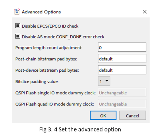
Set the advanced option
Fig 3. 4 Set the advanced option
- Click SDF Data, and then Add File, find *.sof file in the output_files. See Fig 3. 5
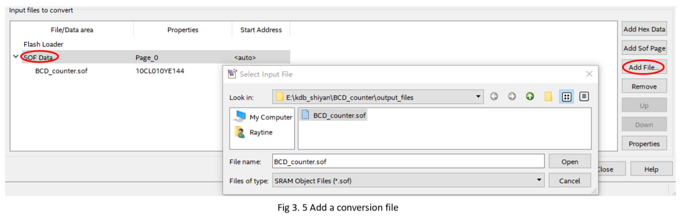
Add a conversion file
Fig 3. 5 Add a conversion file
- Add device. See Fig 3. 6
-
Click Generate, and BCD_counter.jic file will be generated.
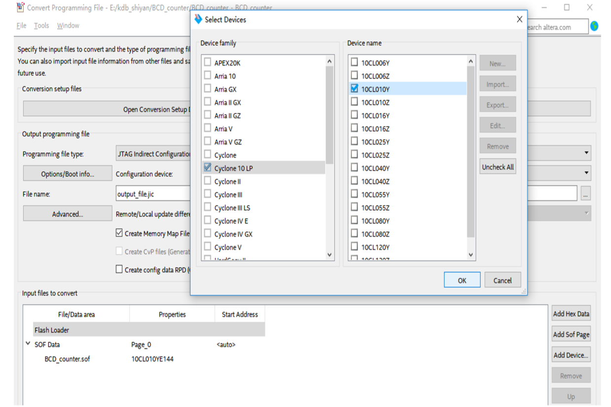
Fig 3. 6 Add device
Fig 3. 6 Add device
- Follow the same downloading procedure in previous experiments. Observe the segment decoder on develop board.