Switch and Use SignalTap II Logic Analyzer in Quartus ( Verilog HDL code ), Learn to analyze the captured signals – FPGA for Beginner Tutorial – Experiment 2 – FII-PRA006
2.1 Experiment Objective
- Continue to practice using the develop board
- Use SignalTap II Logic Analyzer in Quartus
- Use FPGA configuration memory to program
2.2 Experiment Requirement
By using SignalTap II, learn to analyze and capture the experimental signals.
2.3 Experiment
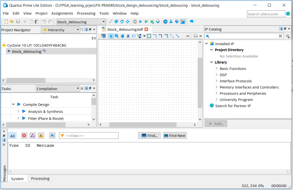
2.3.1 Project Building
Refer to Experiment1, the following experiment project building steps will be eliminated.
2.3.2 PCB Schematics
2.3.3 Experiment Procedure
We include the PLL1 generated in Experiment 1 Verilog HDL code is as follows:
module SW_LED(

input inclk,
input [7:0] sw,
output reg [7:0] led
);

wire sys_clk;
wire pll_locked;
reg sys_rst;

always@(posedge sys_clk)
sys_rst<=!pll_locked;

always @(posedge inclk)
if(sys_rst)
led<=8'hff;
else
led<=~sw;

PLL1 PLL1_INST

(
.areset (1'b0),
.inclk0 (inclk),
.c0 (sys_clk),
.locked (pll_locked)
);

endmodule
2.3.4 SignalTap II Logic Analyzer
Step 1: SignalTap II startup and basic setup
Tools > Signal Tap Logic Analyzer,
-
-
-
-
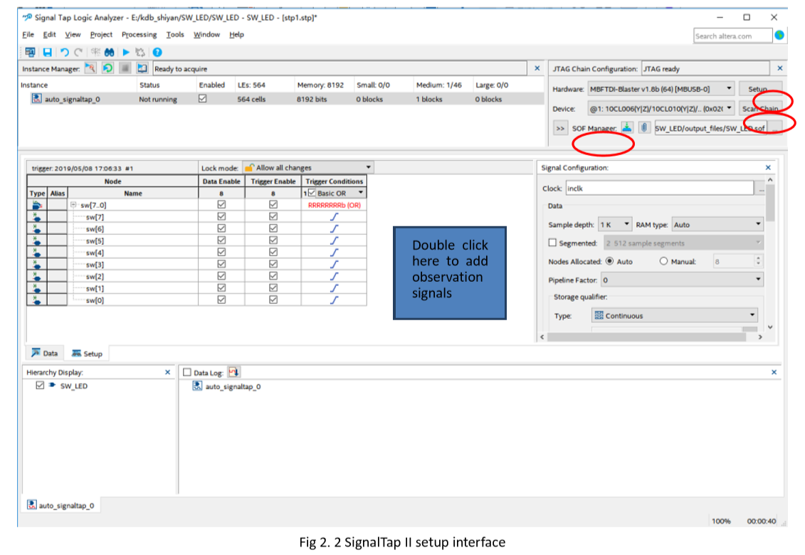
In Fig 2.2, enter the setup interface
-
In JTAG Chain Configuration, click setup to set the same type as the downloader
-
Set the scan chain type
-
Set the SOF Manager, choose the *.sof file generated in Experiment 1
-
-
-
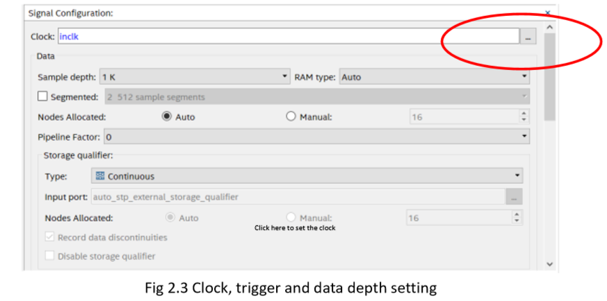
5. Clock setting. See Fig 2. 3
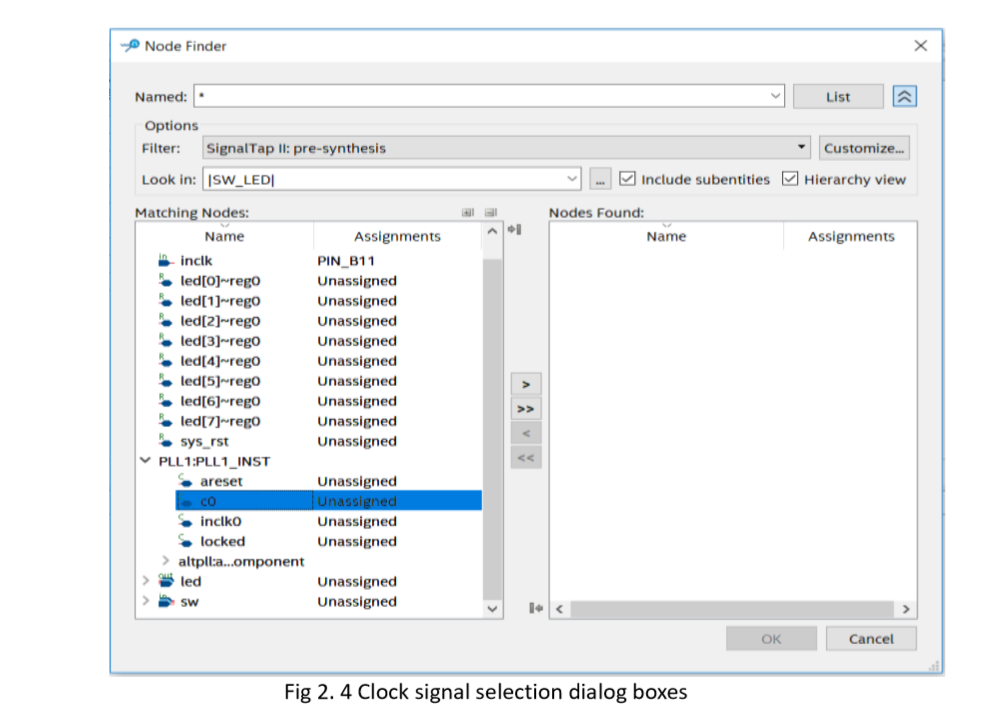
6. In Fig 2. 4, in the popup window, choose SignalTap II: pre-synthesis for Filter,
in Matching Nodes column, go to PLL1: PLL_INST, select c0, and click > to move it to the right frame.
Other settings are shown in Fig 2. 2. For furthermore reference, see the attached file for help.
Step 2: Add the observation signals
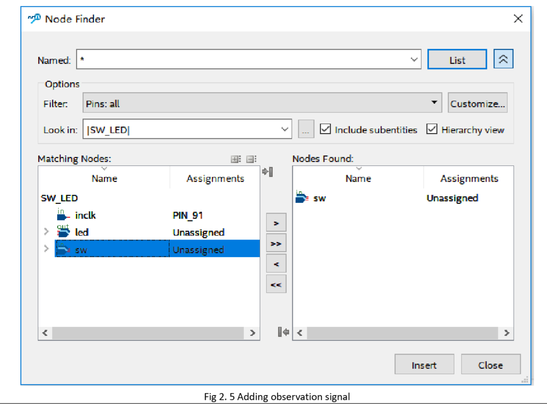
In Fig 2. 2, double click any blank space to add the observation signals.
The interface is shown in Fig 2. 5, choose the signal you want to observe on the left side, click > to add them to the right side, and then click Insert.
Save it and recompile later.
Step 3: Set the observation signals
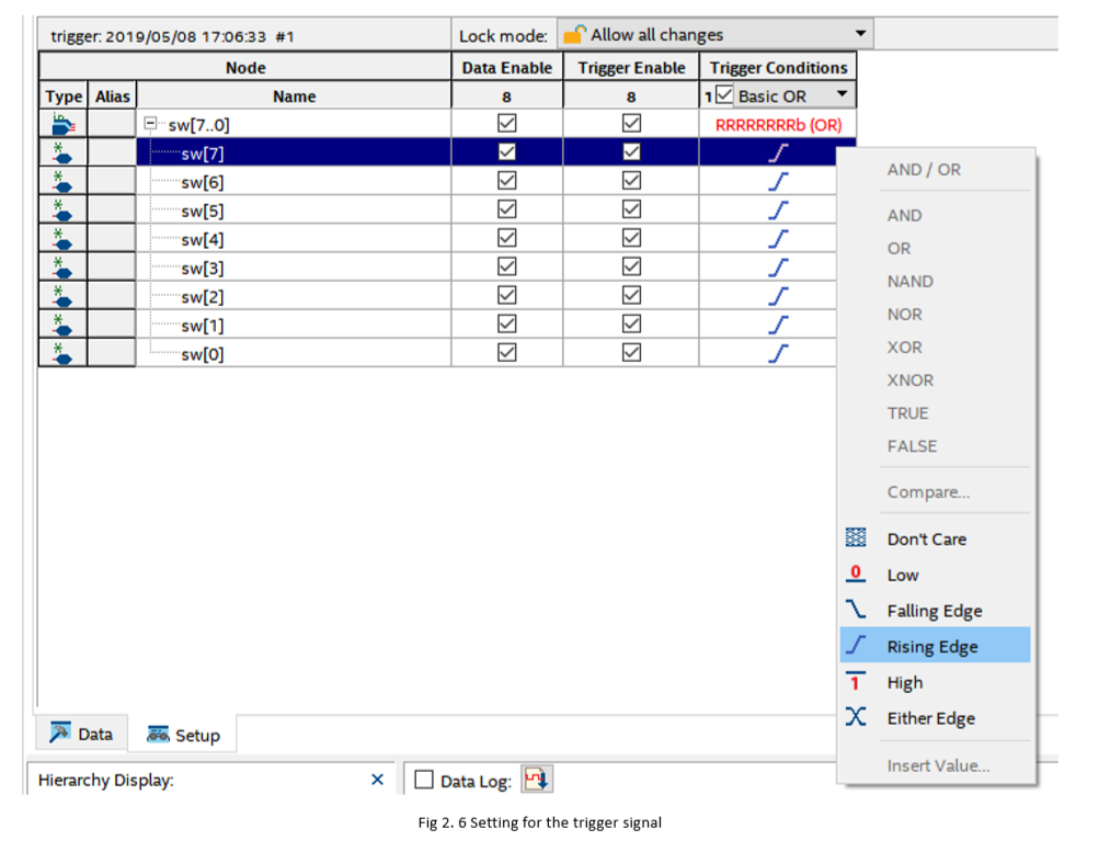
For the observation signals, some settings are still needed, such as whether it is a Rising Edge trigger, a Falling Edge trigger, or Don’t Care, etc. They need to be adjusted manually. See Fig 2. 6.
Step 4: Observe the result
In Fig 2. 7. Run the analysis and observe the SignalTap II output.
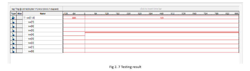
After analysis, when the switch SW [4] is on, the signal is high, and the corresponding LED will be lighted. You could change the trigger type and observe different outputs. Analyze the result and organize it.
The Second Version (2020 – 06- 20 )
Experiment 2 SignalTap
2.1 Experiment Objective
- Continue to practice using of the development board hardware;
- Practice the use of SignalTap Logic Analyzer in Quartus;
- Learn to analyze the captured signals.
2.2 Experiment Implement
Capture and analyze the switching signals on the development board through the use of SignalTap.
2.3 Experiment
2.3.1 Introduction to the Switches and SignalTap
- Introduction to the switches
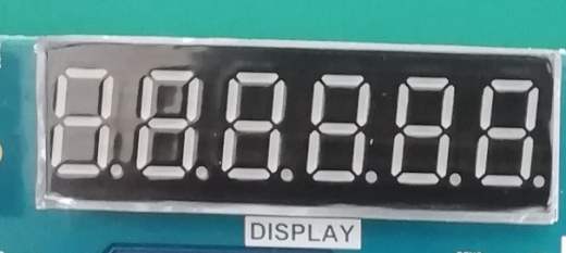
The on-board switch is 8 DIP switches, as shown in Figure 2.1. The switch is used to switch the circuit by turning the switch handle using the binary coding principle of 0/1.
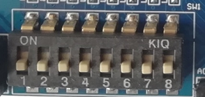
Figure 2.1 DIP switches physical picture
2. Introduction to the SignalTap
SignalTap uses embedded logic analyzers to send signal data to SignalTap for real-time analysis of internal node signals and I/O pins when the system is operating normally.
2.3.2 Hardware Design
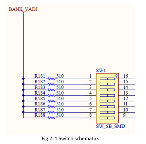
The schematics of the switch is shown in Figure 2.2 (In the red rectangular). One port of the 8 switches is connected to BANK_VADJ at the same time, which is in high level. The other port is respectively connected with an LED, and is connected to the control terminal SW_LED end of the LEDs. When the DIP switch is strobed, the high level turns on the FET, the LED is on, and a high level signal is input to the FPGA at the same time.
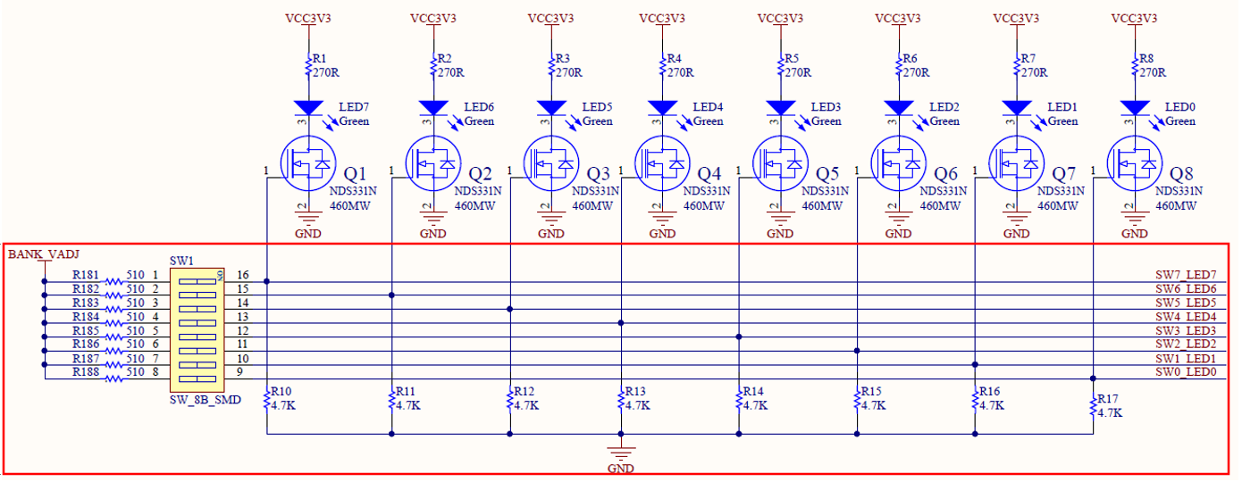
Figure 2.2 Schematics of the switches
2.3.3 Program Design
The first step: the establishment of the main program framework (interface design)
module SW_LED(

input clk,

input [7:0] sw,

output reg [7:0] led

);

endmodule
The experimental input signals have a system clock clk with frequency of 50 MHz, an high effective 8-bit switch sw, and an output 8-bit led.
2.4 Use and Verification of SignalTap Logic Analyzer
The first step: pin assignment
Pin assignments are shown in Table 2.1.
Table 2.1 Pin mapping
| Signal Name | Network Label | FPGA Pin | Port Description |
| clk | C10_50MCLK | 91 | Input clock |
| rst | KEY3 | 10 | Reset |
| SW[7] | SW7_LED7 | 77 | SW 7 |
| SW[6] | SW6_LED6 | 76 | SW 6 |
| SW[5] | SW5_LED5 | 75 | SW 5 |
| SW[4] | SW4_LED4 | 74 | SW 4 |
| SW[3] | SW3_LED3 | 87 | SW 3 |
| SW[2] | SW2_LED2 | 86 | SW 2 |
| SW[1] | SW1_LED1 | 83 | SW 1 |
| SW[0] | SW0_LED0 | 80 | SW 0 |
The second step: SignalTap II setupa dn basic settings
Menu Tools > SignalTap II logic Analyzer,
- In Figure 2.3, set the data under Signal Configuration
- Set the JTAG configuration and click on Setup to set the downloader.
- Set the device type by clicking Scan Chain
- Set up SOF Manager: set as *.SOF that is just compiled and generated before
- Clock and storage depth settings are shown in Figure 2.4.
Click the position shown in Figure 2.4 to add the clock. As shown in Figure 2.5, in the Clock Settings dialog box: Filter select SignalTap: pre-synthesis -> List, select the desired clock signal, select c0 in PLL1: PLL1_INST, move to the box on the right.
Other settings can be set as shown in Figure 2.2. (for advanced use of SignalTap II, please read the Intel reference files)
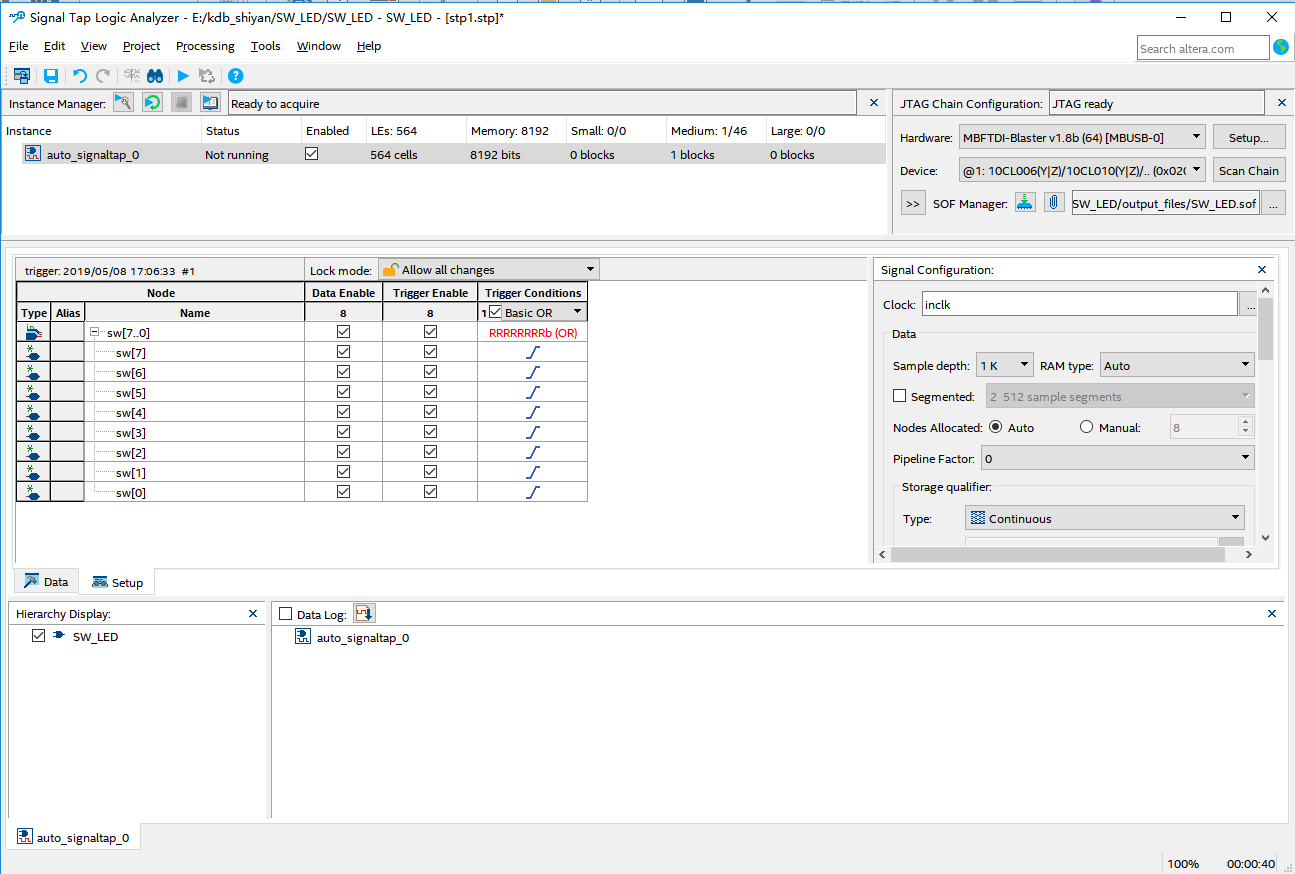
Figure 2.3 SignalTap setting
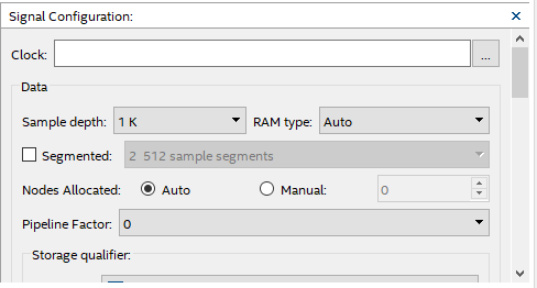
Figure 2.4 Clock signal and the sample depth
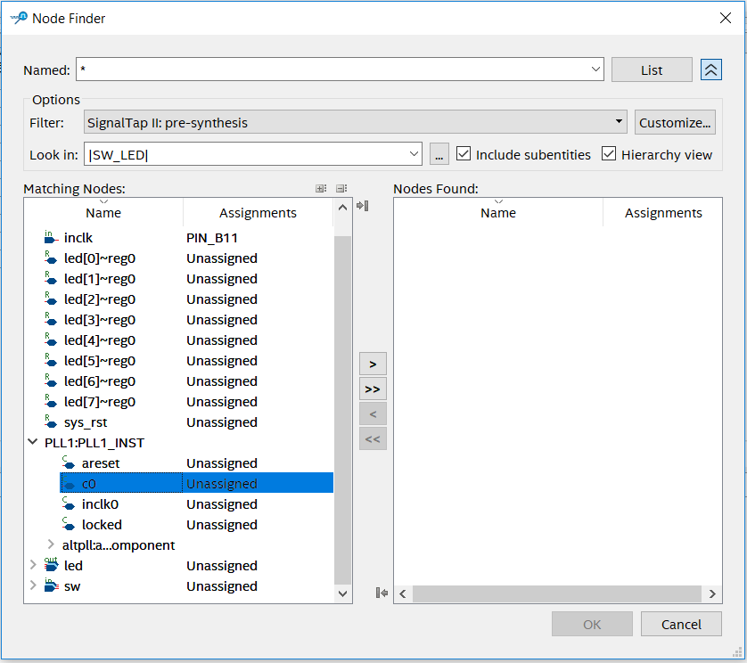
Figure 2.5 Clock signal selection dialogue
The third step: add observation signals
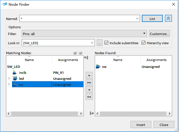
Figure 2.6 Adding interface for the observation signals
As shown in Figure 2.3, double-click the blank space to add the observation signal. Adding interface is shown in Figure 2.6. Select the signal to observe on the left side, add it to the right side, click Insert. Save it and recompile.
The fourth step: setting of observation signals
For the signal to be observed, whether it is a rising edge trigger, a falling edge trigger, or not care, etc., needs to be manually adjusted, as shown in Figure 2.7.
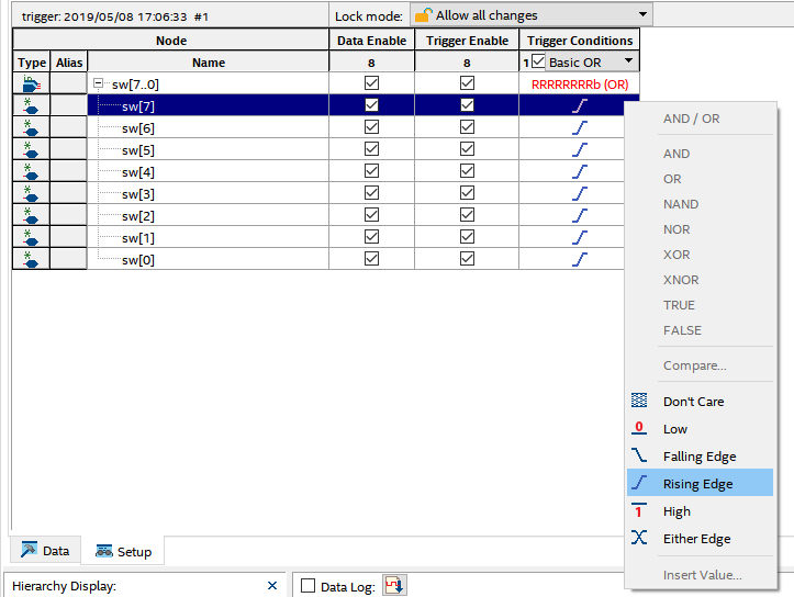
Figure 2.7 Trigger signal setting
The fifth step: observe the result
As shown in Figure 2.8, click Run Analysis to observe the output of SignalTap.
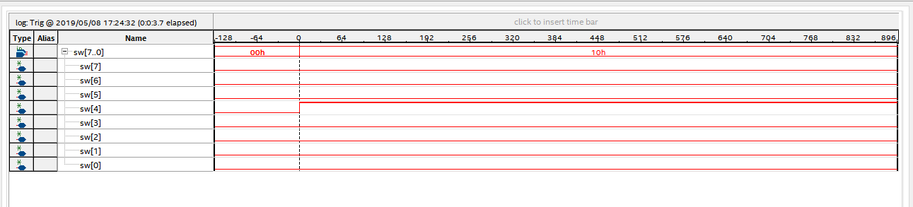
Figure 2.8 Experiment result
After the switch sw[4] is turned on, its signal is high, and the corresponding LED will be lit.
Modify the Trigger condition, test the output results under different Trigger conditions, analyze and summarize the experiment results.