Building new FPGA projects in Quartus, device selection, PLL setup, PLL frequency setting, Verilog’s tree hierarchy design, and the use of SignalTap II – FPGA Board for Beginner – Experiment 4 -PRA006
Experiment 4 Block/SCH Experiment
4.1 Experiment Objective
- Review building new FPGA projects in Quartus, device selection, PLL setup, PLL frequency setting, Verilog’s tree hierarchy design, and the use of SignalTap II
- Master the design method of graphics from top to bottom
- Combined with the BCD_counter project to achieve the display of the digital clock
- Observe the experimental results
4.2 Experiment Implement
Use schematics design to build the project
4.3 Experiment
This experiment is mainly to master another design method. The other design contents are basically the same as the experiment 3. Similar steps will not be introduced in detail. The modular design method is introduced below.
- New project: File -> New Project Wizard…
Project name: block_counter
Select device (10cl010YE144c8G)
- Create new file; File -> New, select Block Diagram/Schematic File. See Figure 4.1.
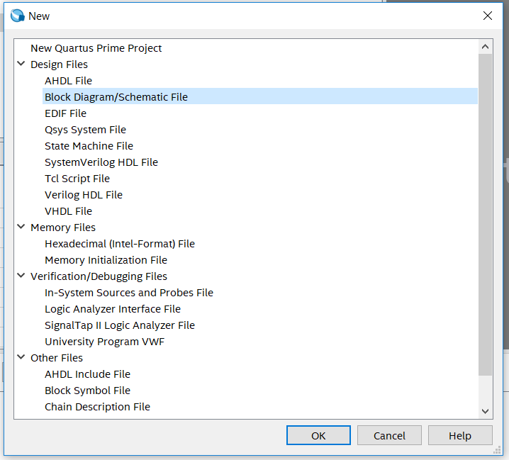
Figure 4.1 New file
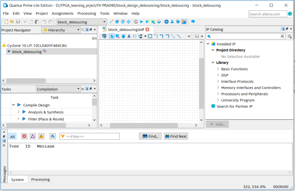
- See Figure 4.2, the middle part is the graphic design area, which can be used for Block/SCH design.
- Save the file as block_counter.bdf
- Double-click the blank space in the graphic design area to add a symbol
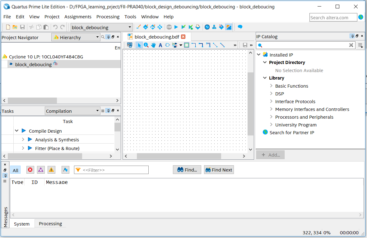
Figure 4.2 Graph design interface
- Graph editing
Double-click on the graphic design area to select the appropriate library and device in the libraries
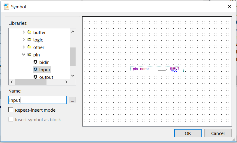
Figure 4.3 Input symbol
- Add input, output, and modify their names
- Add a custom symbol
- bdf Create a new block/sch file and save it as PLL_sys.bdf
- Add PLL IP, refer to experiment 1
- Select the generated file to include the PLL1.bsf file
- Double-click in the blank area of the PLL_sys.bdf file to select the PLL1 symbol just generated and add it to the file, as shown in Figure 4.4.
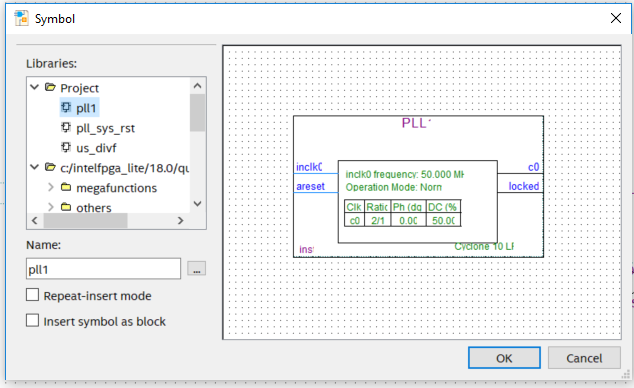
Figure 4.4 Invoke the symbols generated in the IP catalog in the graphical editing interface
- Continue to add other symbols, input, output, dff, GND, etc. and connect them, as shown in Figure 4.5.
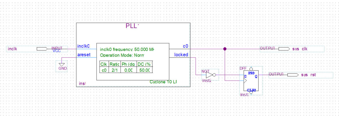
Figure 4.5 Connect the device
- Recreate the newly created file symbol for graphic editing to use in subsequent design
- File > Create/Update > Create Symbol file for Current File. See Figure 4.6.
- Generate PLL_sys.bsf
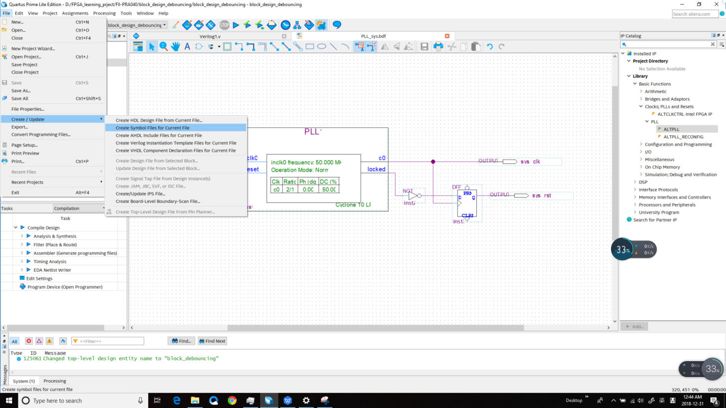
Figure 4.6 Creating a symbol file for the current file (symbol file *.bsf)
- Create a frequency division module
- Create a new verilog file div_us for the frequency divider (Refer project files for the code)
- The PLL output clock is used as its own input clock, and the 100 MHz clock is divided into 1 MHz clocks.
- Repeat (7) to create div_us.bsf
- Create a new 1000 frequency division verilog file: div_1000f.v
- Create div_1000f.bsf symbol
- Create the output pulse us, ms, second module, as shown in Figure 4.7. Refer the specific implementation to the reference code and the frequency division design of the experiment 1 and 3
- Create a new block/sch file block_div and add the designed graphic symbol file to block_div.bdf
- Repeat (7) to create the block_div.bsf symbol
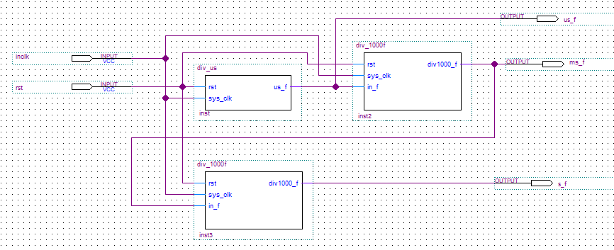
Figure 4.7 us, ms, second pulse of block/sch design
- Create a new verilog file bcd_counter.v, design the hour and minute counter, and create the bsf symbol. Refer to the previous experiments, and implement part of the frequency division using block_div in (9).
- Combine each *.bsf and complete the design of the digital clock (block_counter.bdf), as shown in Figure 4.8.
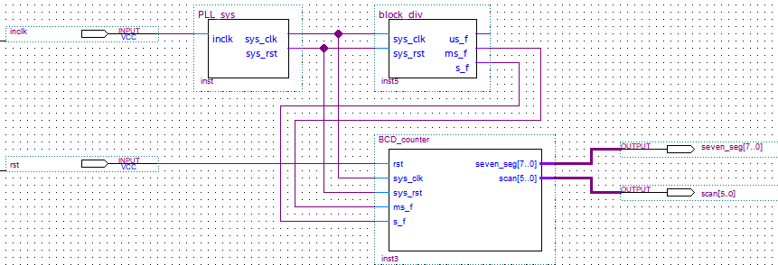
Figure 4.8 Digital clock for BDF design
4.4 Experiment Verification
Pin assignment, compilation, and program verification are consistent with Experiment 3. For reference, see Experiment 3, which is skipped here.
Old Manual ( 2019 version )
4.1 Experiment Objective
-
Review the new project building, PLL setting, Verilog HDL’s tree hierarchy design, use of SignalTap
-
Use graphics method top-down design
-
Combine the BCD_counter design to realize the display of the digital clock
-
Observe the experiment result
4.2 Experiment
-
Build new project named block_counter
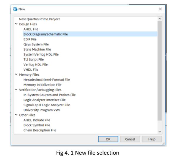
New file selection
Fig 4. 1 New file selection
-
In Fig 4. 1, choose Block Diagram/Schematic File this time instead of Verilog HDL file.
-
In Fig 4. 2, the middle blank part is for designing block diagram or schematics.
-
-
Save the file as block_counter.bdf.
-
Double click the bank space to add the symbol.
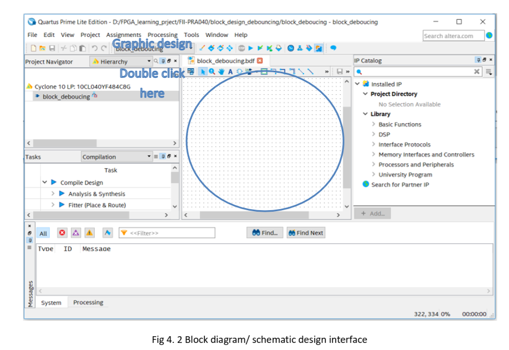
Block diagram/ schematic design interface
-
Fig 4. 2 Block diagram/ schematic design interface
-
In Library, find c:/, and the primitives, or just simply type the symbol name in the search box.
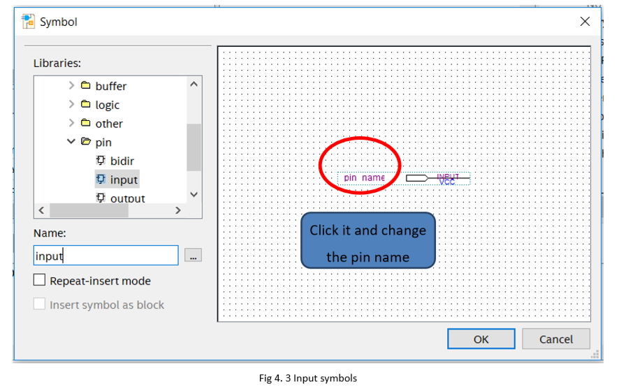
Input symbols
Fig 4. 3 Input symbols
-
Add input and output and modify their names. See Fig 4. 3
-
Add a customized symbol
-
-
Add a new Block Diagram/Schematic File. Save the file as PLL_sys.bdf
-
Create a new PLL I referring to Experiment 1.
-
Select the new generated file to include PLL1.bsf file.
-
Double click blank space in PLL_sys.bdf, and choose under Project, add PLL1. See Fig 4. 4
-
Continue to add other symbols, such as input, output, dff, GND etc. Remember to modify their names. You could choose the Orthogonal node tool icon to wire them. See Fig 4. 5
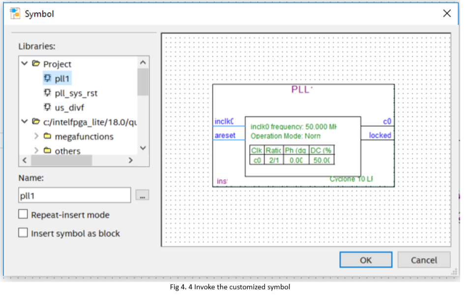
Invoke the customized symbol
-
Fig 4. 4 Invoke the customized symbol
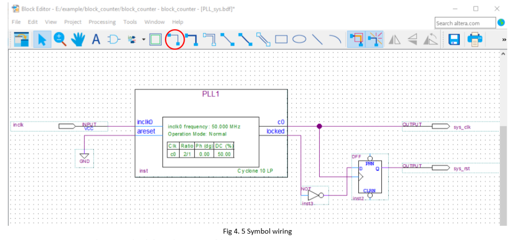
Fig 4. 5 Symbol wiring
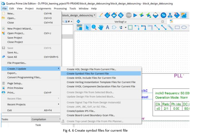
- Create the symbol for the new file
-
- File > Create/ Update > Create Symbol Files for Current File. See Fig 4. 6
- Save as PLL_sys.bsf
Create symbol files for current file
Fig 4. 6 Create symbol files for current file
-
Create a new Verilog HDL file for the frequency division (see reference project files)
-
-
Create a new frequency divider Verilog HDL file named div_us
-
Set PLL output clock as its own input clock. Divide the clock of 100 MHz into a clock of 1 MHz.
-
Repeat step 7, create div _us.bsf
-
Create a new Verilog HDL file with a frequency of 1000: div_1000f.v.
-
Create a div_1000f.bsf symbol
-
-
Create a graph of us, ms, and second output pulse files for testing. See Fig 4. 7
-
-
Create a new Block Diagram/Schematic File, and add this generated symbol to block_div.bdf.
-
Repeat step 7 and create symbol file for block_div.bdf as well.
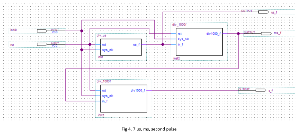
us, ms, second pulse
-
Fig 4. 7 us, ms, second pulse
-
Create a new Verilog HDL file named bcd_counter.v. Design time, minute counter and create bsf symbol. Refer Experiment 3 and implement some of the division using block_div.
-
Combine each *.bsf and complete the design of the digital clock (block_counter.bdf). For the output, use Orthogonal Bus Tool to wire. See Fig 4. 8
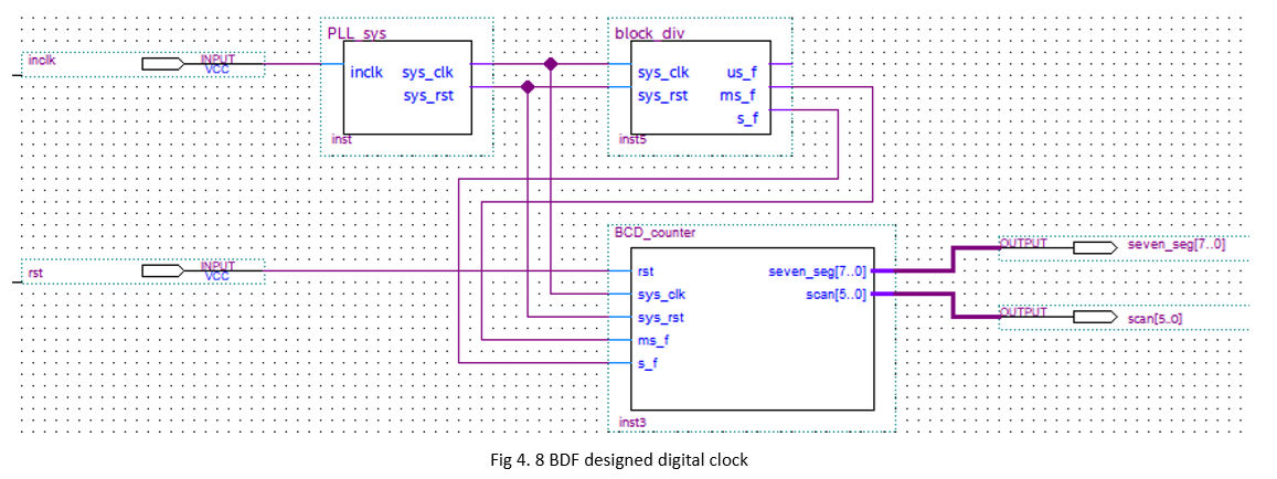
BDF designed digital clock
Fig 4. 8 BDF designed digital clock
- Assign pins, and program it. For the board downloading, you can refer to Experiment 3.